]Permanent address: Department of Synchrotron Radiation, Lund University, SE-22100 Lund, Sweden
Structural determination of a low-symmetry surface by low-energy electron diffraction and ab initio calculations: Bi(110)
Abstract
The surface structure of Bi(110) has been investigated by low-energy electron diffraction (LEED) intensity analysis and by first-principles calculations. Diffraction patterns at a sample temperature of 110 K and normal incidence reveal a bulk truncated (11) surface without indication of any structural reconstruction despite the presence of dangling bonds on the surface layer. Good agreement is obtained between the calculated and measured diffraction intensities for this complex, low-symmetry surface containing only one mirror-plane symmetry element. No significant interlayer spacing relaxations are found. The Debye temperature for the surface layer is found to be lower than in the bulk, which is indicative of larger vibrational atomic amplitudes at the surface. Meanwhile, the second layer shows a Debye temperature close to the bulk value. The experimental results for the relaxations agree well with those of our first-principles calculation.
pacs:
68.35.Bs,61.14.HgI INTRODUCTION
Characteristic of group V elements, bismuth crystallizes in the rhombohedral A7 structure as a semimetal with a small density of states at the Fermi level.Issi (1979) But interestingly, the surfaces of Bi show very different electronic properties than the bulk. Studies on the Bi(110)Agergaard et al. (2001), Bi(100)Hofmann et al. (2005) and Bi(111)Hengsberger et al. (2000); Ast and Höchst (2001) surfaces have shown that they are much more metallic than the bulk due to a significantly higher density of states at the Fermi level at the surface.Hofmann (2006) It has been found that one significant contribution is from a strong spin-orbit coupling at the surface due to broken inversion symmetry.Agergaard et al. (2001); Koroteev et al. (2004); Pascual et al. (2004); Hofmann (2006)
From a chemical point of view, the creation of a surface requires the breaking of atomic bonds. Covalent bonding plays only a minor role in most metals. Thus the effect of bond-breaking is small and surface properties are similar to those of the bulk, although localized electronic surface states may be present. On semiconductors, creating a surface leaves so-called dangling bonds which should give rise to half-filled and therefore metallic bands. However, it turns out that on most semiconductor surfaces the atoms re-arrange their positions such that the dangling bonds are removed and the surface is again a semiconductor and not a metal.Jona et al. (1979) Semimetals such as bismuth lie in between these two cases. On one hand, a semimetal is close to being a semiconductor since directional bonding is important and the valence and conduction bands are almost separated by a gap. On the other hand, there is a very small overlap between both bands such that the material is formally a metal. This delicate balance between being a metal and a semiconductor depends crucially on the atomic structureShick et al. (1999) and it can be expected to be severely disturbed at the surface.
Detailed structural information on Bi surfaces is so far limited to a recent LEED intensity-vs-voltage (IV) and first-principles study of the Bi(111) surface.Mönig et al. (2005) One important difference between bulk terminated Bi(110) and Bi(111) is that the Bi(110) surface exhibits dangling bonds, while Bi(111) does not. In a pioneering study by Jona,Jona (1967) oxygen adsorption experiments suggest that Bi(110) is noticeably more active than Bi(111). A qualitative analysis of LEED patterns in Jona’s study shows an unreconstructed (11) Bi(110) surface structure. From the bulk structure Jona erroneously concluded that the unit cell (and hence the LEED pattern) should not be exactly rectangular but that the lattice vectors should include an angle slightly different from 90∘. This is not correct, as will become appartent below. The unit cell is rectangular and almost quadratic. A recent scanning tunneling microscopy study by Pascual et al.,Pascual et al. (2004) revealed images of the Bi(110) surface that are consistent with a near-square surface unit cell.
A surface structural analysis of this surface has not been undertaken before because of its very low symmetry. The Bi(110) surface has only one symmetry element, a mirror plane, which makes the LEED-IV analysis challenging. An additional complication for Bi(110) is the close stacking of atomic layers, which requires an initial calculation of the bulk diffraction matrices via the combined space method.van Hove and Tong (1979) To our best knowledge, this situation has not been encountered in LEED-IV analyses.
In this article, we report on a study of the surface structure of clean Bi(110) by quantitative LEED intensity-vs-voltage analysis and ab initio calculations. Experimental diffraction intensities taken at a sample temperature of 110 K under normal incidence have been analyzed by comparison to dynamical LEED calculations. Great care was taken to align the sample considering the low symmetry diffraction pattern. The main structural parameters that were optimized in the LEED-IV analysis include the first 4 interlayer spacings and the Debye temperatures for the first 2 surface layers. Furthermore, we have performed first-principles calculations for the atomic structure of Bi(110). The results are in good agreement with the experimental relaxations. The Bi(110) surface can serve as an example for the application of LEED intensity analysis to low symmetry systems.
II BULK TRUNCATED BI(110) SURFACE STRUCTURE
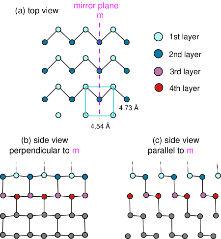
The A7 (Arsenic) structure of bulk bismuth has a rhombohedral unit cell with a two-atom basis. The bulk truncated surface structure of Bi(110) is shown in Fig. 1. The side views show the bilayer stacking with a single bond connecting every other atom between neighboring bilayers. Within one bilayer, each atom in one layer bonds with two nearest-neighbor atoms in the other layer. The covalent bonds have been drawn by solid lines and the dangling bonds at the surface layer by dashed lines. The bilayer-type structure gives rise to alternating interlayer distances. For the truncated bulk at 110 K we have: Å, Å, Å, Å, and so on. Interlayer spacings between the th and th bulk layers are indicated as . Noticeably, the Bi(110) surface has very low symmetry: the only symmetry element is a mirror plane as indicated in Fig. 1. The lengths of unit vectors at 110 K are taken as 4.731 Å and 4.538 Å; see Refs. Cucka and Barrett, 1962; Jona, 1967; Liu and Allen, 1995. If the rhombohedral structure is treated as a pseudocubic structure as in Ref. Jona, 1967, Bi(110) will be denoted as Bi(100). The pseudo-square character of the surface unit cell is evident: for a cubic Bi structure all the atoms in the first bilayer would have the same height, the unit cell would be rotated by about 45∘, and contains only one atom.
III METHODS
III.1 Experimental
The experiment was performed in a -metal ultrahigh vacuum chamber equipped with a four-grid LEED optic with a base pressure of 710-9 Pa. Surface contamination was measured by Auger Electron Spectroscopy (AES) using a hemispherical electron analyzer and the LEED electron gun as electron source. The sample was mounted on a manipulator, allowing positioning to within around all three axes of the crystal. The sample was cooled by liquid nitrogen. The surface was cleaned by cycles of 1 keV Ar+ sputtering and annealing to C. With AES no surface contamination could be detected. The maximum possible oxygen contamination was determined to be 0.02 monolayers. Spot intensities were measured using a 16 bit Charge-Coupled Device (CCD) camera. A back-illuminated and Peltier cooled (C) CCD chip guaranteed a high quantum efficiency and low dark current. The camera was mounted on a base, which allowed rotation around all three axes. Great care was taken to align the camera with respect to the electron gun and the Bi crystal, as described below.
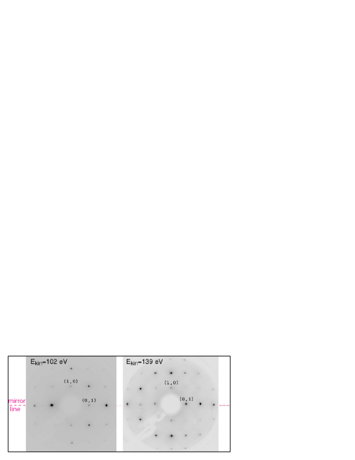
To obtain intensities of the diffracted beams as a function of electron energy, the following procedure was employed: A series of images was recorded within the energy range from 30 eV to 300 eV, while the energy was increased in steps of 1 eV after every recorded image. The integrated spot intensity of every single diffracted beam was extracted from these images. The presence of only one mirror line symmetry for Bi(110) leads to technical challenges for the LEED experiment. These difficulties are illustrated in Fig. 2 that shows two measured LEED patterns taken at different incident energies. The pseudo-square pattern of the reciprocal lattice and the missing left/right symmetry are clearly evident. The up/down symmetry is given by the mirror plane in the crystal (the horizontal plane in Fig. 2). It is necessary to align the sample surface perpendicular to the incoming electron beam, and this is usually done by comparing the IV curves of the symmetry-equivalent beams. Here this procedure can only be applied for the up/down angle. In order to align the left/right angle we optimized the diffraction spot position on the LEED screen until they agreed with the kinematically calculated positions. We estimate that this approach leads to an error of less than in the angle of incidence. In the final data set, the intensities of the symmetry-equivalent beams were averaged.
III.2 Dynamical LEED calculations
The dynamical LEED intensity calculations were performed using the standard package SATLEED (Symmetrized Automated Tensor LEED) by A. Barbieri and M.A. Van HoveBarbieri and van Hove within the renormalized forward scattering perturbation formalism. Atomic scattering phase shifts have been calculated using a muffin-tin potential model and the standard Barbieri and Van Hove phase shift package.Barbieri and van Hove The bulk diffraction matrices for the closely spaced bilayers were calculated with the combined space method.van Hove and Tong (1979) The same muffin-tin radius of 2.87 a.u. and phase shifts have been used as in Ref. Mönig et al., 2005. Phase shifts have been renormalized by the thermal effects of root-mean-square (rms) isotropic vibrational amplitudes. Up to 15 () phase shifts have been used because of the strong scattering of the heavy Bi atom (). The muffin-tin constant is taken to be energy-independent and is optimized. , the imaginary part of inner potential, also referred to as damping potential or optical potential, is taken as 4 eV for the bulk and 4.2 eV for the first 2 overlayers. The slightly larger value at the surface was chosen to model the presence of dangling bonds, which increases the electron damping. The surface potential step of height is located half a long bulk interlayer spacing away from the topmost layer nuclei. The bulk Debye temperature is fixed at 119 K, Jezequel et al. (1984) while the Debye temperatures for the first 2 layers are optimized. Mean-square atomic vibrational amplitudes at temperature for the Debye-Waller factor calculation are derived from Debye temperatures according to the following equation: Pendry (1974)
| (1) |
where is the atomic mass, Planck’s constant and the Boltzmann constant.
In the LEED intensity analysis, agreement between experimental and calculated LEED intensities is quantified by the widely used Pendry factor, , which is particularly sensitive to relative peak position and the existence of small peaks.Pendry (1980) The uncertainties in the optimized structural parameters are estimated from the variation around the minimum ,
| (2) |
where is the total energy range compared in the IV analysis.Pendry (1980)
III.3 Ab initio calculations
We have also performed ab initio calculations of the surface crystal structure of Bi(110). The full-potential linearized augmented plane wave method in film-geometryKrakauer et al. (1979); Wimmer et al. (1981) as implemented in the FLEUR-code was used and the local density approximationMoruzzi et al. (1978) to the density functional theory was employed. Spin-orbit coupling was included in the self-consistent calculations.Li et al. (1990) The evaluation of the surface relaxation has been carried out for the symmetric 14-layer film, both, with the inclusion of the spin-orbit coupling (SOC) term and without this term. Force calculations have been performed for the first four layers without spin-orbit coupling while relaxations have been carried out only for the first two interlayer spacings with the inclusion of SOC. In the latter evaluations we kept the interlayer spacings and equal to those obtained from the force calculation without SOC. The geometry was chosen such, that both sides of the film were terminated with an intact bilayer. A wavefunction cutoff of 3.8 a.u.-1 was chosen and the Brillouin zone was sampled with 32 k-points.
IV RESULTS AND DISCUSSIONS
IV.1 LEED structure determination
The LEED pattern of Bi(110) has previously been discussed by Jona.Jona (1967) He defined a pseudo-cubic bulk unit cell and concluded that the unit cell (and hence the LEED pattern) should not be exactly rectangular but that the lattice vectors should include an angle slightly different from 90∘. Our study does not confirm this conclusion. Our LEED patterns as presented in Fig. 2 show an exact rectangular net from careful measurements of the diffraction spots positions and, indeed, such an exact rectangle can also be expected from a projection of the bulk reciprocal lattice onto the surface.Hofmann (2006) The measured ratio of the two reciprocal unit cell vectors is 0.96(2) in good agreement with the expected value of 0.959. Moreover, the observed patterns show no indication of any reconstruction of the Bi(110) surface, despite the existence of active dangling bond at the surface. Apparently, Bi(110) is found to be very different from typical semiconductors surfaces, such as Si(100) and Ge(100) which both exhibit 21 reconstructions.
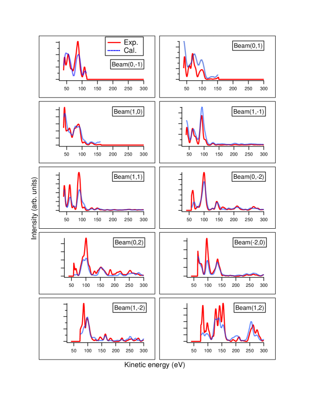
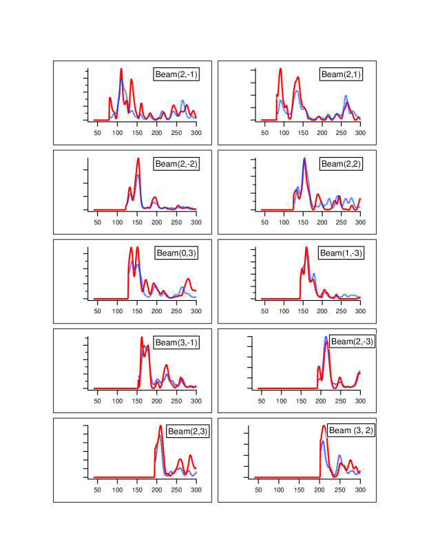
The structural and non-structural parameters were optimized for a Bi(110) surface terminated by an intact bilayer. A termination with a split bilayer was immediately excluded due to lack of agreement with the experimental IV curves shown in Figs. 3 and 4. 20 symmetry in-equivalent beams with a total energy range of 3591 eV have been analyzed to determine the following structural and non-structural parameters: the first four interlayer spacings (; ), the real part of inner potential , and Debye temperatures and for atoms in the first and second layers, respectively. The results of the structural analysis are summarized in Table 1. Note that the first and the third interlayer spacing correspond to the small separation (0.21 Å) between the two layers making up the bilayer in the bulk. Their seemingly dramatic relative relaxations are very small in absolute terms. Also, the forth layer appears to move above the third layer by 0.01 Å. However this very small value is clearly below our detection limit. Overall no significant relaxation for the Bi(110) surface is found. We have tried many possible displacement patterns allowed due to the low surface symmetry. However, we found no significant improvement in when changing the relative distance between the two basis atoms in the first and second layer parallel to the mirror line. The Debye temperature for the first layer is found to be lower than that of the bulk, which is consistent with an early study of Goodman and Somorjai.Goodman and Somorjai (1970) Reduced surface Debye temperatures are a common phenomenon reflecting the weaker bonding of surface atoms compared to the bulk.Walfried et al. (1996) The actual numerical values of the surface Debye temperature are an important ingredient for the determination of the electron-phonon coupling strength from angle-resolved photoemission data.Ast and Höchst (2002); Gayone et al. (2005); Kim et al. (2005) Meanwhile the second layer shows a Debye temperature close to the bulk value.
| Parameters | Starting values | Optimized values | (%) |
|---|---|---|---|
| (eV) | 8.0 | ||
| (Å) | 0.208 | ||
| (Å) | 3.064 | ||
| (Å) | 0.208 | ||
| (Å) | 3.064 | ||
| (K) | 119 | ||
| (K) | 119 | ||
The LEED-IV analysis gives a relatively high factor of about 0.455 compared to typical values of 0.1 to 0.3 for clean unreconstructed metal surfaces. We believe it is due to the structural complexity and low symmetry of the Bi(110) surface and it is not caused by deviations from normal incidence during the IV measurement. We simulated non-normal incidence conditions extensively in the LEED-IV calculations and found that an increase in the incident angle gave a dramatic rise in the factor from its minimum at zero or normal incidence. This shows that the sample is properly aligned. As seen on open semiconductor surfaces the presence of dangling bonds and the presence of voids in the open surface structure is a real challenge for the muffin-tin approximation of the crystal potential and could also contribute to the relatively high for this surface. However, the low surface symmetry of Bi(110) gives rise to the large number of non-equivalent beams. The good agreement between this large experimental data set and the calculated intensity-energy curves, as shown in Figs. 3 and 4, give us great confidence in the reliability of our results.
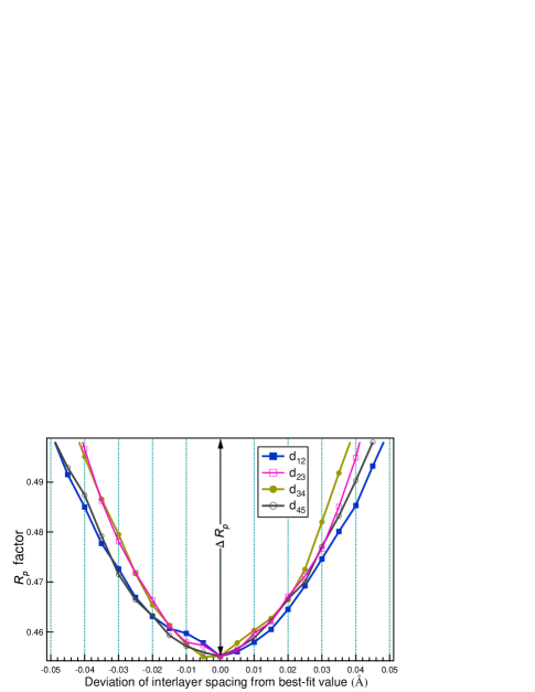
The error bars of the optimized parameters were analyzed based on the variation the factor around , = 0.043 according to Eq. 2. The dependence of on a change of the interlayer spacings away from their optimized values is shown in the Fig. 5. In this analysis, all other parameters were fixed at their optimized values. We can see that all the sensitivity curves take on a parabolic shape. The errors for the individual parameters are also listed in the Table 1.
IV.2 Comparison to first-principles calculations
The first-principle calculations performed for bulk Bi without the inclusion of spin-orbit interaction give bulk short and long interlayer spacings of 0.142 Å and 3.087 Å, respectively. Evaluations that include the SOC term lead to a very slight modification of approximately 0.01 Å of these results. Our scalar relativistic force calculations give the following values for the first 4 interlayer spacing relaxations at 0 K: %, %, %, and %. These results agree reasonably well with those obtained by the LEED-IV analysis at 110 K (see Table 1) considering the fact that the absolute distance difference between the experimental and calculated first interlayer relaxations of % and % is only 0.06 Å. Both the experiment and theory lead to the contraction of the first interlayer spacing. For the second interlayer spacing the theory gives a small expansion while the experiment shows a small contraction of the spacing. However the theoretical result is within the experimental error bar. The absolute distance difference between the experimental and calculated second interlayer relaxations of 0.015 Å is even smaller than that for the first interlayer spacing. For the third and fourth interlayer spacings the theory and experiment are in excellent agreement. The first-principle calculations that include the spin-orbit interaction term lead to % and % for the first and second interlayer spacings respectively. These values have been obtained by keeping the interlayer spacings and equal to those found in the scalar relativistic calculations. This shows that the influence of spin-orbit interaction on the relaxation is small and probably will not change the values of and significantly. Notice, that in the relaxed geometry a change of % or Å in corresponds to an energy change of only 0.5 meV per surface atom which is certainly at the limit of our accuracy.
In our force calculations, we also optimized the position of the surface atoms in a plane parallel to the surface. By symmetry, this movement is then confined to the mirror plane shown in Fig. 1 (a). We notice, that these relaxations are small and do not exceed % in the top four layers, consistent with the experimental findings.
V Conclusions
Our results give a consistent picture of the very low-symmetry surface geometric structure of Bi(110) by LEED intensity analysis and first-principles calculations. Good agreement is reached between experimental LEED and theoretical IV curves. No structural reconstruction occurs despite of dangling bonds present at the surface. No significant absolute value of relaxation is found for the first 4 interlayer spacings. The reduced top-layer Debye temperature suggests essentially larger vibrational atomic amplitudes at the surface. Experimentally, the approach of sample alignment by calculating the diffraction spot positions on the LEED screen is very efficient and can be used for surfaces with low symmetry as well as for in-situ cleaved surfaces.
Acknowledgements.
This work was supported by the American National Science Foundation DMR-0134933, the Danish National Science Foundation, the Basque Country Government, and by the University of the Basque Country.References
- Issi (1979) J.-P. Issi, Australian Journal of Physics 32, 585 (1979).
- Agergaard et al. (2001) S. Agergaard, C. Søndergaard, H. Li, M. B. Nielsen, S. V. Hoffmann, Z. Li, and P. Hofmann, New Journal of Physics 3, 15.1 (2001).
- Hofmann et al. (2005) P. Hofmann, J. E. Gayone, G. Bihlmayer, Y. M. Koroteev, and E. V. Chulkov, Physical Review B 71, 195413 (2005).
- Hengsberger et al. (2000) M. Hengsberger, P. Segovia, M. Garnier, D. Purdie, and Y. Baer, The European Physical Journal B 17, 603 (2000).
- Ast and Höchst (2001) C. R. Ast and H. Höchst, Phys. Rev. Lett. 87, 177602 (2001).
- Hofmann (2006) P. Hofmann, Progress in Surface Science 81, 191 (2006).
- Koroteev et al. (2004) Y. M. Koroteev, G. Bihlmayer, J. E. Gayone, E. V. Chulkov, S. Blügel, P. M. Echenique, and P. Hofmann, Phys. Rev. Lett. 93, 046403 (2004).
- Pascual et al. (2004) J. I. Pascual, G. Bihlmayer, Y. M. Koroteev, H.-P. Rust, G. Ceballos, M. Hansmann, K. Horn, E. V. Chulkov, S. Blügel, P. M. Echenique, et al., Phys. Rev. Lett. 93, 196802 (2004).
- Jona et al. (1979) F. Jona, H. D. Shih, D. W. Jepsen, and P. M. Marcus, J. Phys. C: Solid State Phys. 12, L455 (1979).
- Shick et al. (1999) A. B. Shick, J. B. Ketterson, D. L. Novikov, and A. J. Freeman, Physical Review B 60, 15484 (1999).
- Mönig et al. (2005) H. Mönig, J. Sun, Y. M. Koroteev, G. Bihlmayer, J. Wells, E. V. Chulkov, K. Pohl, and P. Hofmann, Physical Review B 72, 085410 (2005).
- Jona (1967) F. Jona, Surface Science 8, 57 (1967).
- van Hove and Tong (1979) M. A. van Hove and S. Y. Tong, Surface Crystallography by LEED (Springer-Verlag, Berlin, 1979).
- Cucka and Barrett (1962) P. Cucka and C. S. Barrett, Acta. Cryst. 15, 865 (1962).
- Liu and Allen (1995) Y. Liu and R. E. Allen, Phys. Rev. B 52, 1566 (1995).
- (16) A. Barbieri and M. A. van Hove, packages available online: http://www.sitp.lbl.gov/index.php?content=/leedpack/leedpack.html.
- Jezequel et al. (1984) G. Jezequel, A. Barski, P. Steiner, F. Solal, P. Roubin, R. Pinchaux, and Y. Petroff, Physical Review B 30, 4833 (1984).
- Pendry (1974) J. B. Pendry, Low Energy Electron Diffraction (Academic Press, London, 1974).
- Pendry (1980) J. B. Pendry, J. Phys. C 13, 937 (1980).
- Krakauer et al. (1979) H. Krakauer, M. Posternak, and A. J. Freeman, Phys. Rev. B 19, 1706 (1979).
- Wimmer et al. (1981) E. Wimmer, H. Krakauer, M. Weinert, and A. J. Freeman, Phys. Rev. B 24, 864 (1981).
- Moruzzi et al. (1978) V. L. Moruzzi, J. F. Janak, and A. R. Williams, Calculated Electronic Properties of Metals (Pergamon, New York, 1978).
- Li et al. (1990) C. Li, A. J. Freeman, H. J. F. Jansen, and C. L. Fu, Phys. Rev. B 42, 5433 (1990).
- Goodman and Somorjai (1970) R. M. Goodman and G. A. Somorjai, J. Chem. Phys. 52, 6325 (1970).
- Walfried et al. (1996) C. Walfried, D. N. McIlroy, J. Zhang, P. A. Dowben, G. A. Katrich, and E. W. Plummer, Surface Science 363, 296 (1996).
- Ast and Höchst (2002) C. R. Ast and H. Höchst, Phys. Rev. B 66, 125103 (2002).
- Gayone et al. (2005) J. E. Gayone, C. Kirkegaard, J. W. Wells, S. V. Hoffmann, Z. Li, and P. Hofmann, Applied Physics A 80, 943 (2005).
- Kim et al. (2005) T. K. Kim, T. S. Sorensen, E. Wolfring, H. Li, E. V. Chulkov, and P. Hofmann, Physical Review B 72, 075422 (2005).