[
Synthesis of VO2 Nanowire and Observation of the Metal-Insulator Transition∗
Abstract
We have fabricated crystalline nanowires of VO2 using a new
synthetic method. A nanowire synthesized at 650∘C shows
the semiconducting behavior and a nanowire at 670∘C
exhibits the first-order metal-insulator transition which is not
the one-dimensional property. The temperature coefficient of
resistance in the semiconducting nanowire is 7.06 /K at 300 K,
which is higher than that of commercial bolometer.
] One dimensional (1-D) nanostructure materials exhibit unique physical properties that differ from their bulk properties. It is due to a characteristic of the 1-D structure such as nanotubes, nanorods, and nanowires [1-3]. It is well-known that an abrupt metal-insulator transition (MIT) and a hysteresis behavior do not occur in 1-D structure. These are an advantage for a device application. Therefore, synthetic efforts for 1-D materials have been continued by many researchers, although synthesis of 1-D structures is very difficult.
The transition oxide material, VO2, undergoes the structural phase transition (SPT) from the monoclinic to the rutile tetragonal structures near 340 K. It was revealed that the first-order MIT is controlled by hole doping of a low density and is not caused by the SPT; this demonstrated the Mott transition [4]. VO2 has a lot of applications such as electro-optic switch, infrared bolometer, and the Mott first-order field effect transistor (FET), etc. New ideas for the first-order MIT transistor were disclosed by Kim and Kang [5] and Chudnovski et al. [6]. For the fabrication of nanometer-scale Mott FET devices, the synthesis of single-crystalline VO2 nanowires was reported [7]. Metastable VO2 nanowire arrays were synthesized via an ethylene glycol reduction approach [8].
In this paper, we reports synthesizing conditions of VO2 nanowires fabricated by using a synthetic method. Their electrical characteristics are analyzed by measuring the temperature dependence of resistance and I-V characteristics. In particular, to our knowledge, we first observed first-order MITs in nanowires.
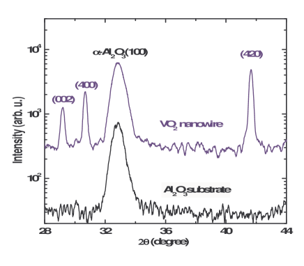
VO2 nanostructures with nanoblock and nanowire were successfully synthesized by controlling the oxygen partial pressure in the oxidation process of metallic vanadium. The metallic vanadium was grown on -Al2O3 (01-10) substrate at 500∘C in an Ar ambient atmosphere of 50 mTorr using RF Sputter. Advantage of this new method is a shorter synthesis time than that of other nanowire fabrication methods such as thermal chemical vapor deposition [9] and the bulk crystal growth method [6]. The use of Al2O3 substrate different from SiO2/Si derived more high quality nanowire on the basis of the fact that VO2 film is well-grown on Al2O3. Annealing was performed at 630670∘C in the O2 ambient atmosphere of 50 mTorr for 3060 minutes. Figure 1 shows an X-ray diffraction (XRD) pattern of the crystal structure of a VO2 nanowire grown at 630∘C for 30 minutes. Lattice constants from XRD peaks are calculated as a=12.03 , b=6.693 , c=6.42 , which is in agreement with the reported values of the monoclinic VO2 for JCPDS (card No. 71-0042) [10]. (400) peak is the most intense peak of typical VO2 thin film grown on -Al2O3 substrate. The XRD peaks indicate that the VO2 nanowire is crystalline.
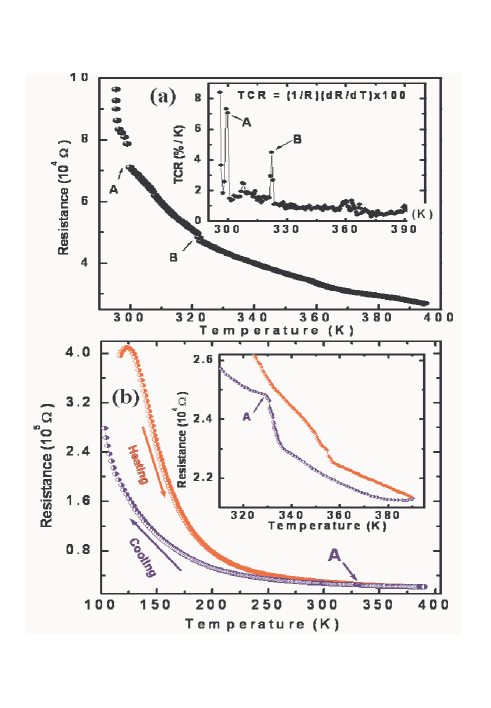
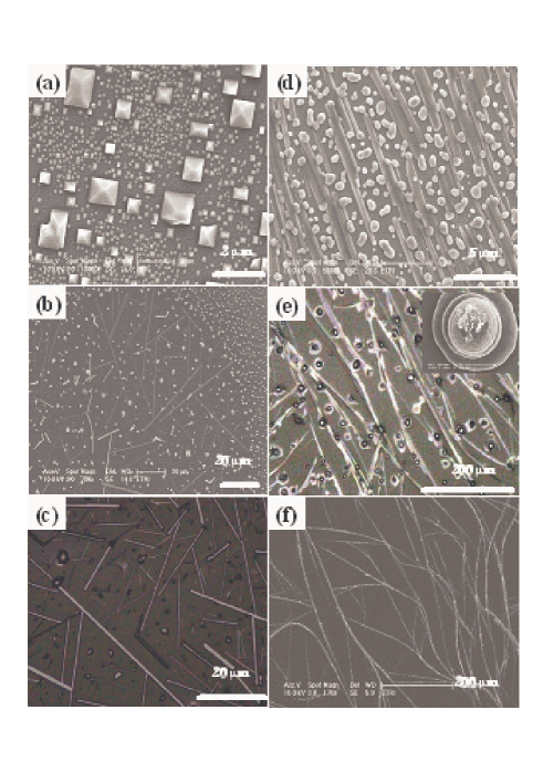
Figure 2 (a)(c) show high resolution scanning electron microscopy (SEM) images of nanostructures synthesized at several annealing temperatures. The nanostructures are the semblance nanoblocks (quadrangular pyramid) and nanowires. Nanoblocks with a size of 50 500 nm were synthesized at 630∘C. Nanoblocks and wires coexist at 650∘C. Only nanowires were grown at 670∘C. The nanowires in Fig. 2(c) are rectangular parallelepiped form with a length of 10800 m (z-axis), a width of 20150 nm (y-axis) and a thickness of 100500 nm (x-axis).
Annealing time for fabrication of good nanowires was also changed from 40 to 60 minutes with step of 10 minute, as shown in Fig. 2 (d)(f). When annealing time was 40 min (Fig. 2(d)), nanowires begin to connect with a neighbor nanowire, and it appear a small nanoblock like a cone form. The inset in Fig. 2(e), it shows a clearly cone form. Annealing time was 1 hour, a nanowire is connected to other nanowires like a crooked bough, as shown in Fig. 2(f). Thus, the optimum growth condition of VO2 nanowires on Al2O3 substrate is found to be at 670∘C and 30 min.
We measured the temperature dependence of resistance and I-V characteristic curves to reveal electrical properties of VO2 nanowires. Figure 3 shows the temperature dependence of resistance and hysteresis curve for the VO2 nanowires grown at 650∘C. The temperature dependence is semiconductive and has no the MIT jump (abrupt change in resistance with temperature) which is the resistance characteristic of VO2. Moreover, the temperature coefficient of resistance (TCR) has large values near 300 K and below 320 K (inset in Fig. 3 (a)). A TCR value at 300 K is 7.06 /K, which is larger than that of a commercial bolometer, as indicated by arrow A in Fig. 3(a). A TCR peak near 320 K is due to a change of the resistance near 320 K, as indicated by arrow B. Figure 3(b) shows a lower resistance than that at 300 K in Fig. 3(a) and the semiconducting temperature behavior in the heating process. Hysteresis in the heating and cooling process is exhibited. In the cooling process, a small step of the resistance near 330 K appears, as indicated by arrow A in the inset of Fig. 3(b), which can be regarded as the first-order MIT in VO2. This is attributed to hole excitation by heating produced in the cooling process from a high temperature of 390 K, on the grounds that the first-order MIT occurs by hole excitation [4]. The fact that the magnitude of the jump is small is due to a large resistance in the nanowire because the large resistance reduces the magnitude of jump [5].
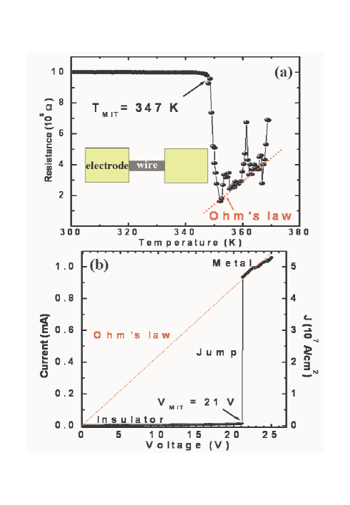
For the VO2 nanowire grown at 670∘C, the sharp first-order MIT jump near 347 K and the ohmic behavior above 347 K are exhibited (Fig. 4(a)). The electric field-induced first-order MIT is also measured (Fig. 4(b)). Jump of Current is 1.210-5 A to 910-4 A at VMIT=21V and current follows Ohm’s law in the larger voltage than VMIT. This indicates that the nanowire has a component of metal. The MIT voltage can be controlled by varying the distance between electrodes of nanowire. The observed first-order MITs are attributed to breakdown of the critical on-site Coulomb interaction between electrons [4,11].
In summary, we found conditions fabricating nanowires showing the first-order MIT which is far from the 1-D structural property. Furthermore, the crystalline nanowires with large resistnace are useful to a lot of device applications.
REFERENCES
- [1] This was presented in NANOMAT 2006 ”International workshop on nanostructed materials” on June 21-23th of 2006 in Antalya/TURKEY.
- [2] sungyoul@etri.re.kr
- [3] Z. R. Dai, Z. W. Pan, and Z. L. Wang, Adv. Funct. Mater. 13, 9 (2003)
- [4] Greta R. Ratzke, Frank Krumeich, Reinhard Nesper, Angew. Chem. Int. Ed. 41, 2446 (2002).
- [5] Nicola Pinna, Marc Willnger, Klaus Weiss, Joachim Urban, Robert Schlogl, Nano Lett. 3, 1132 (2003).
- [6] H. T. Kim, B. G. Chae, D. H. Youn, S. L. Maeng, G. Kim, K. Y. Kang, and Y. S. Lim, New J. Phys. 6, 52 (2004).
- [7] H. T. Kim, K. Y. Kang, US patent 6,624,463, Priority: Sept. 2001.
- [8] Chudnovski, F., Luryi, S., B. Spivak, ”In Future Trends in Microelectronics: the Nano Millenium” (A. Zaslavsky. Ed., Wiley-Interscience, New York, 2002) pp148-155.
- [9] B. S. Guiton, Q. Gu, A. L. Prieto, M. S. Gudiksen, and H. Park, J. Am. Chem. Soc. 127, 498 (2005).
- [10] X. Chen, X. Wang, Z. Wang, J. Wan, J. Liu, and Y. Qian, Nanotechnloogy 15, 1685 (2004).
- [11] Z. R. Dai, Z. W. Pan, Z. L. Wang, J. Am. Chem. Soc. 124, 8673 (2002).
- [12] F. Theobald, R. Cabala, J. Bernard, J. Solid State Chem. 17, 431 (1976).
- [13] H. T. Kim, Physica C341-348 (2002) 259; ’New Trends in Superconductivity’ NATO Science Series II Vol. 67 p137 (Eds, J. F. Annett and S. Kruchinin, Kluwer, 2002); cond-mat/0110112.