Nature of Spin Hall Effect in a finite Ballistic Two-Dimensional System with Rashba and Dresselhaus spin-orbit interaction
Abstract
The spin Hall effect in a finite ballistic two-dimensional system with Rashba and Dresselhaus spin-orbit interaction is studied numerically. We find that the spin Hall conductance is very sensitive to the transverse measuring location, the shape and size of the device, and the strength of the spin-orbit interaction. Not only the amplitude of spin Hall conductance but also its sign can change. This non-universal behavior of the spin Hall effect is essentially different from that of the charge Hall effect, in which the Hall voltage is almost invariant with the transverse measuring site and is a monotonic function of the strength of the magnetic field. These surprise behavior of the spin Hall conductance are attributed to the fact that the eigenstates of the spin Hall system is extended in the transverse direction and do not form the edge states.
pacs:
72.25.Dc, 72.10.-d, 73.50.JtIntroduction: The Hall effect (from now on we refer as the charge Hall effect) is a well-known important phenomena in condensed matter physics. It occurs due to the Lorentz force that deflects like-charge carriers towards one edge of the sample creating a voltage transverse to the direction of current. Recently, another interesting phenomena, the spin Hall effect (SHE), has been discovered and has attracted considerable attentions. Here, a spin accumulations emerge on the transverse sides of the sample, when adding a longitudinal electric field or bias. If external leads are connected to the sides, the pure transverse spin current is generated. The SHE can either be extrinsic due to the spin dependent scatteringHirsch ; extrinsic or intrinsic due to the spin-orbit (SO) interaction. The intrinsic SHE is predicted first by Murakami et.al. and Sinova et.al. in a Luttinger SO coupled 3D p-doped semiconductorZhangsc and a Rashba SO coupled two-dimensional electron gas (2DEG)Niuq , respectively. After that a number of recent works have focused on this interesting issue.Inoue ; Mishchenko ; Rashba1 ; Yao ; Jiang ; Chalaev ; Bernevig ; Sheng ; Marinescu ; add1 ; Hankiewicz ; Branislav ; Reynoso ; Branislav1 ; add2 For an infinite system, it was pointed out that the spin Hall conductivity is very sensitive to disorder,Inoue ; Mishchenko ; Rashba1 ; Yao ; Jiang ; Chalaev ; Bernevig and the SHE vanishes even in a very weak disorder. On the other hand, in the finite mesoscopic ballistic system, the SHE can survive.Sheng ; Marinescu ; add1 ; Hankiewicz ; Branislav ; Reynoso ; Branislav1 By using the Landauer-Büttiker formalism and the tight-binding HamiltonianDattabook ; Pareek , the SHE and spin polarization have been studied in the dirtySheng ; Marinescu ; add1 or cleanHankiewicz ; Branislav ; Reynoso mesoscopic samples. These investigations show that the SHE is still present below a critical disorder. Experimentally, the SHE is observed on n-type GaAs Kato and on p-type GaAs Sinova , where the transverse spin accumulations are detected by Kerr rotation spectroscopy or the circularly polarized light-emitting diode, respectively.
In this paper, we study the nature of the SHE in a finite 2DEG, and mainly focus on the comparison between the SHE and the charge Hall effect. This is because the SHE and the charge Hall effect are so analogous, intuitively they should have similar properties. In the charge Hall effect, the Hall voltage is a universal constant along the transverse edge, i.e. it is independent of the transverse measuring location and the width of device. At least its sign is unchanged. Does the spin current possess similar universal behavior in SHE? The results are very surprising and show that the transverse spin current in the SHE is strongly dependent on the measuring location and the device’s shape.add3 Not only the intensity but also its sign can change. These results indicate that the SHE is not as clean as the charge Hall effect, and all the measured quantity in SHE are very sensitive on the details of the system. We attribute these no-universal behaviors to the extensive eigenstates in the transverse direction in the SHE.
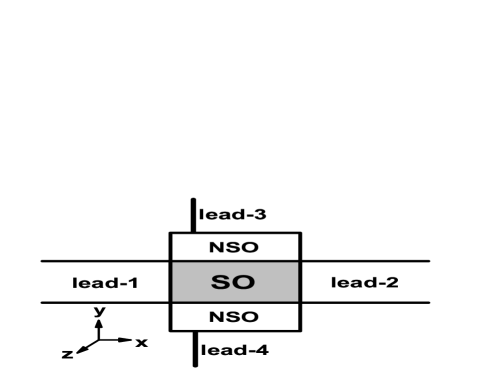
model and formulation: The system we considered is shown in Fig.1 which consists of a finite central ballistic region attached to four semi-infinite leads. The Rashba and Dresselhaus SO interactionsRashba are present only in the central gray rectangular region with the size . In order to study the geometric effect, two zero-SO coupling (NSO) zones (central white regions in Fig.1) with the size are also patched. All the leads are assumed to be clean and ideal, without any SO coupling. The two longitudinal leads (lead-1 and lead-2) have the width , which are the same as the width of the central SO region. On the other hand, in order to study the local spin Hall conductance and its dependence on the measuring location, two transverse leads (lead-3 and lead-4) are assumed to be one-dimensional (1D) with the width , and they can be coupled to any edge location along the direction.
The above system can be described by the Hamiltonian , where and are the coefficient of the Rashba and Dresselhaus SO interactions.Rashba Then in the tight-binding representation, this Hamiltonian can be written as:Sheng ; Marinescu
| (5) | |||||
| (10) | |||||
| (11) |
where is the hopping matrix element with the lattice constant . In order for the band-width of the 1D lead-3 and lead-4 to be in the same range of to , the hopping matrix element in these two leads are set to be . Here and represent the strength of the Rashba and Dresselhaus interactions, respectively, and and are non-zero only in the central gray region. and in Eq.(1) are the unit vectors along the and directions.
Since there is no SO interactions in the leads, the spin in the leads are a good quantum number and the definition of the spin current is unambiguous. Then the particle current in the lead- (, , , and ) with spin index (, or stands for the or direction) can be obtained from the Landauer-Büttiker formula: , Pareek ; Dattabook where is the bias in the lead- and is the transmission coefficient from the lead- with spin to the lead- with spin . The transmission coefficient can be calculated from , where the line-width function , the Green’s function , Dattabook and is the retarded self-energy. After solving , the spin current and the charge current can be obtained straightforwardly: and . The terminal voltages are set as: and , i.e. a longitudinal bias is added between the lead-1 and the lead-2. The transverse lead-3 and lead-4 act as the voltage probes, and their voltages and are calculated from the condition . Then the transverse spin Hall conductances are: and . For comparison, we also calculate the transverse charge currents or the charge conductances ( and ) in the same device but under a different condition instead of . In the numerical calculation, we take which is near the band bottom , and as a energy unit, then the corresponding lattice constant .Branislav1 The device’s sizes (i.e. , , and ) are chosen in the same order with the spin precession length over the precessing angle . Here . If taking , then .
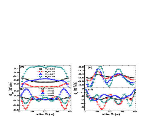
Numerical results and discussion: First, we consider the case that the center region has only Rashba interaction () and two NSO zones do not exist with . While , it can be shown that and . The spin Hall conductance versus the measuring sites and are depicted in Fig.2a and Fig.3a. We see that depends on the location of measuring sites , and it can even change its sign, e.g., when (see Fig.2a). On the other hand, at the fixed measuring site with different , the curve of versus can also cover the range from negative to positive (see Fig.3a). In contrast to the charge Hall effect, their behaviors are essentially different. The Hall voltage or the charge Hall conductance usually are monotonously increasing functions of the strength of the external magnetic field. Furthermore they usually are unchanged with the transverse measuring sites.

Next, we attach two NSO zones to the system (see Fig.1). For the charge Hall effect, the charge accumulates in the transverse boundaries. If two zones having no magnetic field are attached, the charge accumulation will naturally transfer from the original boundaries to the new one, as a result the Hall voltage and the charge Hall conductance do not change much. How is the spin Hall conductance affected when two NSO zones are attached? Fig.2b and Fig.3b show, respectively, versus the site and for different thickness of the NSO zone. The results show that the spin Hall conductance is strongly affected by the NSO zones. For example, in the curves -, for or (see Fig.2) is flat, and it is negative at all site . With increasing , shows an oscillation behavior. In particular, can be positive, i.e. change its sign, for some value of (e.g. ). In the curve of versus it also exhibits the similar results that is strongly dependent on including changing its sign (see Fig.3b).
For comparison, we also show the charge conductance for the same system but different bias conditions (see Fig.2c,d). We see that is always negative and exhibits an oscillation behavior. For (i.e. without the NSO zones), is weakly dependent on the site , whereas for , the oscillatory amplitude of increases slightly. In particular, the charge conductance is nearly ten times larger than the spin Hall conductance . This also means is much smaller than the universal value , where is the channel number, and in the present device because that the lead-3’s and lead-4’s width is . Notice that in the charge Hall effect, the Hall conductance usually takes the universal value .
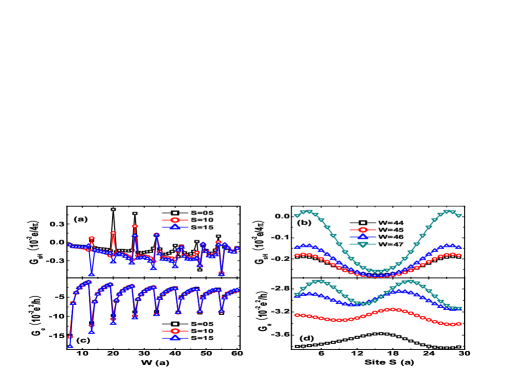
Let us study the spin Hall conductance versus the transverse width of the center SO’s regions. and versus exhibit almost periodic peaks (see Fig.4a,c). Note that the cutoff energy of the subband (i.e. the transverse energy levels) are about , which shifts down with increasing the width . For the Fermi level across a subband, a jump emerges in the curves of - (or -), due to the large density of state near the band edge. As a result for a given period (e.g. =44, 45, 46, and 47), and versus the site (see Fig.4b,d), exhibit the oscillation behavior. As the Fermi level across the subband edge (=47), can change its sign while are always negative.
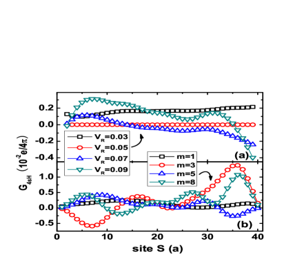
In the following, we investigate the case when the Dresselhaus SO interaction is present, i.e. . As mentioned above, at the spin currents through the lead-3 and lead-4 are conserved, i.e., . However, when and , . On the other hand, the spin Hall conductance has the symmetry with due to the symmetry of our system. It is worth to point out when , , which is similar with the Ref.(14). In the Fig.5, versus the site for different or different width of the NSO zone are plotted. Here exhibits similar characters as in the case of : is very sensitive to the transverse measuring site , and it can even changes its sign (e.g. ). While , oscillates with the site along with the variation of its sign. All these behaviors are in contrast to the charge Hall conductance.
Finally, we emphasize that the sensitivity of spin Hall conductance to the location of measuring sites is a generic feature not due to the 1D nature of the lead-3 and lead-4. We have performed similar calculations when the width of lead-3 and lead-4 are and . The conclusion remains. In addition, if the lead-3 and lead-4 are placed at two different measuring sites along x-direction, and are affected even stronger.
Why are the characters of the SHE so different with the charge Hall effect? Why is the spin Hall conductance so sensitive (even its sign) to the measurement site , the shape of device, and so on? We attribute them to following two reasons. (1). In the quantum Hall effect the edge states emerge and play an important role. However for a system that exhibits SHE, e.g., the quasi 1D quantum wire having Rashba SO interaction, its eigen states are extended in the transverse direction and they do not form edge states.sun (2). The force in the charge Hall effect always points to a specific direction, e.g. . But the force in the SHE is dependent on the spin , and its sign can vary.shen
In summary, the spin Hall conductance is strongly dependent on the transverse measuring site, the device’s shape, and the strength of the spin-orbit interaction. Not only the magnitude but also its sign can change. These characters are very different from that of the charge Hall effect, and the spin Hall conductance is not universal as the charge Hall conductance.
Acknowledgments: We gratefully acknowledge helpful discussions with Prof. H. Guo. This work was supported by NSF-China under Grant Nos. 90303016, 10474125, and 10525418. J.W. is supported by RGC grant (HKU 7044/05P) from the government SAR of Hong Kong.
References
- (1) Electronic address: sunqf@aphy.iphy.ac.cn
- (2) J.E. Hirsch, Phys. Rev. Lett. 83, 1834 (1999).
- (3) M.I. Dyakonov and V.I. Perel, JETP Lett. 13, 467 (1971); Phys. Lett. A 35, 459 (1971).
- (4) S. Murakami, N. Nagaosa, and S.C. Zhang, Science 301, 1348 (2003); Phys. Rev. B 69, 235206 (2004).
- (5) J. Sinova, D. Culcer, Q. Niu, N.A. Sinitsyn, T. Jungwirth, and A.H. MacDonald, Phys. Rev. Lett. 92, 126603 (2004).
- (6) J.I. Inoue, G.E.W. Bauer, and L.W. Molenkamp, Phys. Rev. B 70 ,041303(R) (2004).
- (7) E.G. Mishchenko, A.V. Shytov, and B.I. Halperin, Phys. Rev. Lett. 93, 226602 (2004).
- (8) E.I. Rashba, Phys. Rev. B 70, 201309(R) (2004).
- (9) Y. Yao and Z. Fang, Phys. Rev. Lett. 95, 156601 (2005); G.Y. Guo, Y. Yao, and Q. Niu, ibid., 94, 226601 (2005).
- (10) Z.F. Jiang, R.D. Li, S.-C. Zhang, and W.M. Liu, Phys. Rev. B 72, 045201 (2005).
- (11) O. Chalaev, and D. Loss, Phys. Rev. B 71, 245318 (2005).
- (12) B.A. Bernevig, and S.C. Zhang, Phys. Rev. Lett. 95, 016801 (2005); R. Raimondi and P. Schwab, Phys. Rev. B 71, 033311 (2005).
- (13) L. Sheng, D. N. Sheng, and C.S. Ting, Phys. Rev. Lett. 94, 016602 (2005); L. Sheng, D. N. Sheng, C.S. Ting, and F.D.M. Haldane, ibid., 95, 136602 (2005).
- (14) C.P. Moca, and D.C. Marinescu, Phys. Rev. B 72, 165335 (2005).
- (15) J. Li, L. Hu, and S.-Q. Shen, Phys. Rev. B 71, 241305(R), (2005).
- (16) E.M. Hankiewicz, L.W. Molenkamp, T. Jungwirth, and J. Sinova, Phys. Rev. B, 70, 241301(R) (2004).
- (17) B.K. Nikoli, L.P. Zrbo, and S. Souma, Phys. Rev. B 72, 075361 (2005).
- (18) A. Reynoso, Gonzalo Usaj, and C.A. Balseiro, cond-mat/0511750.
- (19) B.K. Nikoli, S. Souma, L.P. Zrbo, and J. Sinova, Phys. Rev. Lett. 95, 046601 (2005); J. Yao and Z.Q. Yang, Phys. Rev. B 73, 033314 (2006); J. Wang, K.S. Chan, and D.Y. Xing, Phys. Rev. B 73, 033316 (2006).
- (20) J. Schliemann and D. Loss, Phys. Rev. B 71, 085308 (2005); X. Dai, Z. Fang, Y.-G. Yao, and F.-C. Zhang, Phys. Rev. lett. 96, 086802 (2006).
- (21) Chapter 2 and 3, in Electronic Transport in Mesoscopic Systems, edited by S. Datta (Cambridge University Press 1995).
- (22) T.P. Pareek, Phys. Rev. Lett. 92, 076601 (2004).
- (23) Y.K. Kato, R.C. Myers, A.C. Gossard, and D.D. Awschalom, Science 306, 1910 (2004); V. Sih, R.C. Myers, Y.K. Kato, W.H. Lau, A.C. Gossard, and D.D. Awschalom, Nature Phys. 1, 31 (2005).
- (24) J. Wunderlich, B. Kaestner, J. Sinova, and T. Jungwirth, Phys. Rev. Lett. 94, 047204 (2005).
- (25) The spin accumulation is also strongly influenced by boundary conditions for both extrinsic and intrinic SHE, which has been reported in two recent works: W.-K. Tse, J. Fabian, I. Zutic, and S. Das Sarma, Phys. Rev. B 72, 241303(R) (2005); V.M. Galitski, A.A. Burkov, and S. Das Sarma, cond-mat/0601677.
- (26) Y.A. Bychkov and E.I. Rashba, J. Phys. C, 17, 6039 (1984); G. Dresselhaus, Phys. Rev. 100, 580 (1955).
- (27) In fact, the system of the quasi 1D quantum wire having Rashba SO interaction can exactly be solved, and its eigen states indeed are extended in the transverse direction, e.g. see Q.-f. Sun and X.C. Xie, cond-mat/0505517.
- (28) B.K. Nikolic, L.P. Zarbo, and S. Welack, Phys. Rev. B 72, 075335 (2005); S.-Q. Shen, Phys. Rev. lett. 95, 187203 (2005); K.Yu. Bliokh, cond-mat/0511146.