Electrically-detected magnetic resonance in ion-implanted Si:P nanostructures
Abstract
We present the results of electrically-detected magnetic resonance (EDMR) experiments on ion-implanted Si:P nanostructures at 5 K, consisting of high-dose implanted metallic leads with a square gap, in which Phosphorus is implanted at a non-metallic dose corresponding to . By restricting this secondary implant to a 100 nm 100 nm region, the EDMR signal from less than 100 donors is detected. This technique provides a pathway to the study of single donor spins in semiconductors, which is relevant to a number of proposals for quantum information processing.
pacs:
71.55.-i, 76.30.-v, 85.40.RyThe ability to spectroscopically study the spin properties and interactions of a small number of donors in semiconductors has many applications such as the storage of classical information in nuclear or electronic spins,1 and is relevant to a number of proposals2, 3 related to quantum information processing (QIP). In particular, the construction of QIP hardware utilizing Si:P has been discussed by Kane 4 and Hollenberg.5 In this context, the ultimate task is the detection of the electron or nuclear spin state of single P donors.
The detection of the spin resonance of donors in semiconductors via electron spin resonance (ESR) is well established.6 However, the sensitivity of conventional ESR (where magnetisation is measured) is limited to samples containing donors or more.7 This problem can be overcome by detecting magnetic resonance via the effects of spin selection rules on other observables, such as magnetic force 8, radiative transitions9, or charge transport.10, 11, 12
Electrically detected magnetic resonance (EDMR), where a resonant change of the dc conductivity is monitored12, was first demonstrated on Si:P by Schmidt and Solomon.13 Subsequent studies of P in crystalline Si using EDMR were performed both at very high 14 and very low magnetic fields,15 as well as for P in amorphous16 and microcrystalline17 silicon. Electrical detection of electron-nucleon double resonance (EDENDOR)18 has been successfully demonstrated, also on Si:P. As shown unambiguously by corresponding optically detected magnetic resonance (ODMR) experiments on molecules, the detection of ESR via spin-dependent electronic transitions can be extremely sensitive, ultimately allowing the study of single spins.19, 20 Kawachi and coworkers21 were able to observe EDMR from about dangling bond defects in micron-size amorphous silicon thin-film transistors. Stich et al.18 reported successful detection of P in Si via EDMR in samples containing as few as donors. However, no systematic study into the sensitivity reachable with conventional EDMR experiments on donor states has been published so far, in particular achieving even better detection limits on P-doped silicon. Here, we present the results of a systematic EDMR study of the sensitivity of ion-implanted Si:P on samples where the smallest number of donors in the active area is less than 100.
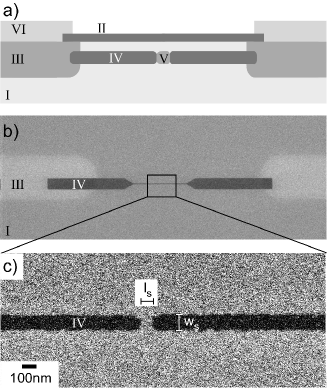
The devices used for this study were fabricated on high resistivity ( 8 kcm, corresponding to donors cm-3) n-type silicon wafers (Fig. 1, label I). First, ohmic contacts for the source and drain leads of the device were defined via phosphorus indiffusion (III). A 5 nm gate oxide (II) was then grown using a wet oxidation process. TiAu (15 nm Ti,65 nm Au) markers, 100 nm 100 nm in dimension, were defined by electron-beam lithography (EBL) and used to align subsequent EBL steps with an accuracy of 50 nm. A 150 nm thick poly-methyl-methacrylate (PMMA) resist was applied and patterned by EBL for use as a mask for ion-implantation of the leads of width (labelled IV in Fig. 1) with P implantation at an ion energy of 14 keV to an areal dose of 1014 cm-2, corresponding to a doping density of cm-3, well above the Mott or metal-insulator transition at . The leads were doped to this density as it has been shown 22 that EDMR of highly doped implanted Si:P does not show any hyperfine split resonance signal. The mean implantation depth is 20 nm at this ion energy. The tip of the leads define an active region (labeled V in Fig. 1), with a distance between the leads.
Using this basic contact geometry, three different devices were fabricated. Type 1: Devices with a secondary P implant covering the whole wafer. This implant was at an energy of 14 keV, with an areal density of 51011 cm-2, giving a maximum doping density of 21017cm-3. Type 2: Devices where this secondary implant is limited to the area between the leads (V) using a PMMA mask. The purpose of this type of sample is to allow quantification of the number of donors being investigated. Type 3: Control samples without secondary implant. Following implantation, a rapid thermal anneal (RTA) at 1000 ∘C for 5 seconds was performed to activate the donors and repair the damage due to implantation23. Afterwards, ohmic contacts are formed by removal of the oxide in the contact region, followed by deposition of Al(80nm)/Au(20nm) metallic contacts.
EDMR measurements were performed in a modified Bruker ESR measurement setup. The sample was illuminated with white light from a halogen lamp, and a DC voltage VDC was applied to one contact (source). The other contact (drain) was connected directly to a current amplifier, and the output of the amplifier was fed into a lock-in amplifier. Microwave radiation at a fixed frequency in the X-band and a power of 50 mW was applied to the circular dielectric cavity. Higher microwave power led to significant microwave-induced currents, most probably due to rectification by asymmetric contacts. The magnetic field was modulated at kHz with an amplitude of 0.3 mT. The external magnetic field was swept over 10 mT in 200 seconds. All spectra shown are corrected to a fixed microwave frequency =9.7 GHz. The field sweep was repeated and the lock-in output averaged to obtain a high signal-to-noise ratio. All measurements reported here were taken at K.
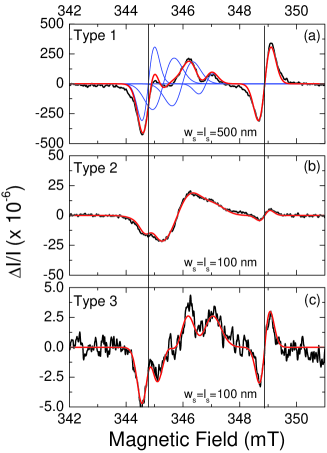
Figure 2 a shows the relative change of the current vs. the external magnetic field for a Type 1 sample with nm. The magnetic field positions of the resonances were obtained by fitting the measured data with five gaussian derivatives, as seen in Fig. 2 a. The two resonances due to the hyperfine splitting of P are clearly visible with the expected 4.2 mT splitting.24 There is also a smaller resonance observable at mT corresponding to , which we attribute to exchange-coupled pairs of P donors.24, 25 Additionally, two resonance lines with -factors of and are observed for the orientation of the sample with . Taking into account the limited resolution at X-band frequencies and the power-induced broadening, these -factors are compatible with and of the defect26 and therefore are attributed to this defect at the Si/SiO2 interface.
Figure 2 b shows the relative current change for a Type 2 device with nm. The number of P implanted into the active region is 508, as determined from the implant parameters. Even with such a small number of phosphorus donors in the active region, an EDMR signal intensity given by the peak-to-peak current change of the high-field hyperfine-split P resonance of is easily detectable. The defect signal observed in the Type 2 samples is dominated by a single resonance at , characteristic for the so-called dangling bond signal also observed at Si/SiO2 interfaces.27
Due to the use of P in the lead fabrication, the effect of the straggle of the lead implantation in contributing donors to the active sample area must be taken into account. Figure 2 c shows the EDMR signal from a Type 3 device, also with nm, where no P is implanted directly into the gap area from a second implant. Also here, the characteristic signature of hyperfine-split P is observable, however with a smaller . This signal is due to the straggle of the leads, which we now consider in detail.
Spin-dependent hopping in Si:P at very high P concentrations has been studied in detail, including samples where P incorporation was obtained by implantation.22, 28 An increase of the dark conductivity was observed under ESR conditions at the central, exchange coupled resonance with 29 for samples above the Mott transition, with typical values for decreasing from at [P] cm-3 to at [P] cm-3.22, 30, 31 Therefore, a contribution from the leads in our experiments will be limited to the central line at due to the high doping concentration. In contrast, hyperfine-split lines can only arise from P in a local concentration below .25 The amount of P with [P] in a Type 3 device with nm in area (V) between the leads and due to straggle can be estimated from SRIM simulations32 for our implantation to be about considering the surface of the leads facing area (V). Finally, due to the overlap of the two implantation processes a total of about P donors in area (V) from the leads and the secondary implant are present in the Type 2 device with nm.
Figure 3 shows the EDMR signal intensity of the P hyperfine-split peak at mT for all types of samples as a function of . Notably, the EDMR intensities of the Type 1 and 2 devices cluster at and at respectively, independent of . Due to Ohm’s law and the quadratic geometry of the gap, the resistance of each type of device studied in a purely drift based model is independent of the characteristic size and therefore the resonant changes in the current should indeed be size independent. This demonstrates that with the restriction of the current path to areas containing few P donors, Pauli-blockade effects lead to an effective influence of the transport properties of the device. Differences in the EDMR signal intensities between the Types are expected due to the different areas implanted with P and the current path not being restricted completely to the gap area. Since we monitor resonant changes in the photoconductivity, diffusive transport and spin-dependent recombination throughout the whole sample cannot be excluded outright. However, the fact that in the control experiments on Type 3 devices, a significant spin-dependent recombination is only observed for the smallest structure length, where the relative contribution of the straggle to the P donors in the active area (V) is largest, clearly indicates that the P donors in the active area contribute most to the EDMR signal, while the recombination near the leads or indiffused contacts only plays a minor part.

Analyzing the signal-to-noise ratio of the spectra measured and determining from them a signal-to-noise ratio for a single magnetic field scan based on Poisson statistics yields a typical for Type 1 and for Type 2 samples, again independent of . If the independence of the signal intensity on the structure length persist also at smaller length, single P donors could be monitored in Type 2 samples with nm at the same ratio. Nevertheless, the sensitivity demonstrated here on devices with as few as 100 donors in the active area surpasses the sensitivity demonstrated for EDMR so far by several orders of magnitude.
Remarkably, the relative signal intensities of the and the P hyperfine-split lines found in our experiments are of the same order of magnitude, independent of the overall signal intensity and the type of the device. This suggests that the spin-dependent recombination process investigated is a P- pair process, where a photogenerated excess electron is captured by a P donor and forms a spin pair with a defect, a process also proposed as a readout scheme for silicon QIP hardware33. Furthermore, P- pair recombination can only occur near the Si/SiO2 interface, and therefore any P donors in the bulk of the sample, underneath the implanted leads and the indiffused contacts do not contribute to the EDMR signal.
Whilst the results shown in Fig. 3 indicate that the signal is in fact due to the low-dose implant into the metallic region, further investigations are warranted. Apart from experiments investigating the influence of the defect density of the Si/SiO2 interface and the fabrication steps leading to the and dangling bond defects on the EDMR signals, devices where the donor species used in the fabrication of the ohmic contacts and leads is different from that in the active area should be studied, so that any resonance signature detected can be attributed to the active area unequivocally. Arsenic lends itself to this purpose, as it has a different hyperfine splitting than phosphorus. Initial measurements on devices with Arsenic leads and ohmic contacts, both fabricated by ion implantation, show behaviour consistent with the results presented here, which shows that the signal is due to the donors implanted into the active region.
We have demonstrated a pathway to the spectroscopic study of a small number of donors in semiconductors, by selective implantation of phosphorus into silicon. We have shown that it is possible to observe the change in conductivity caused by EDMR of less than 100 donors in the active device region. In principle this technique is not restricted to P, but can be extended to other dopants.
We would like to thank A. Ferguson, V. Chan, M. Stutzmann and A. Stegner for helpful discussions and E. Gauja for technical support. This work was supported by the Australian Research Council, the Australian Government and by the US National Security Agency (NSA), Advanced Research and Development Activity (ARDA), the Army Research Office (ARO) under contract number DAAD19-01-1-0653 and by the Deutsche Forschungsgemeinschaft (SFB 631).
References
- Recher et al. 2000 P. Recher, E. V. Sukhorukov, and D. Loss, Phys. Rev. Lett. 85, 1962 (2000).
- Vrijen et al. 2000 R. Vrijen, E. Yablonovitch, K. Wang, H. W. Jiang, A. Balandin, V. Roychowdhury, T. Mor, and D. DiVincenzo, Phys. Rev. A 62, 012306 (2000).
- Schenkel et al. 2003 T. Schenkel, A. Persaud, S. J. Park, J. Nilsson, J. Bokor, J. A. Liddle, R. Keller, D. H. Schneider, D. W. Cheng, and D. E. Humphries, J. Appl. Phys. 94, 7017 (2003).
- Kane 1998 B. E. Kane, Nature 393, 133 (1998).
- Hollenberg et al. 2004 L. C. L. Hollenberg, A. S. Dzurak, C. Wellard, A. R. Hamilton, D. J. Reilly, G. J. Milburn, and R. G. Clark, Phys. Rev. B 69, 113301 (2004).
- Feher 1959 G. Feher, Phys. Rev. 114, 1219 (1959).
- Maier 1997 D. C. Maier, Bruker Rep. 144, 13 (1997).
- Rugar et al. 2004 D. Rugar, R. Budakian, H. J. Mamin, and B. W. Chui, Nature 430, 329 (2004).
- Jelezko et al. 2004 F. Jelezko, T. Gaebel, I. Popa, A. Gruber, and J. Wrachtrup, Physical Review Letters 92, 076401 (2004).
- Elzerman et al. 2004 J. M. Elzerman, R. Hanson, L. H. W. van Beveren, B. Witkamp, L. M. K. Vandersypen, and L. P. Kouwenhoven, Nature 430, 431 (2004).
- Xiao et al. 2004 M. Xiao, I. Martin, E. Yablonovitch, and H. W. Jiang, Nature 430, 435 (2004).
- Brandt et al. 2004 M. S. Brandt, S. T. B. Goennenwein, T. Graf, H. Huebl, S. Lauterbach, and M. Stutzmann, phys. stat. sol. (c) 1, 2056 (2004).
- Schmidt and Solomon 1966 J. Schmidt and I. Solomon, Compt. Rend. (Paris) 263, 169 (1966).
- Honig and Moroz 1978 A. Honig and M. Moroz, Rev. Sci. Inst. 49, 183 (1978).
- Stich et al. 1995 B. Stich, S. Greulich-Weber, and J.-M. Spaeth, J. Appl. Phys. 77, 1546 (1995).
- Brandt and Stutzmann 1991 M. S. Brandt and M. Stutzmann, Phys. Rev. B 43, 5184 (1991).
- Kanschat et al. 2000 P. Kanschat, K. Lips, and W. Fuhs, J. Non-Cryst. Solids 266, 524 (2000).
- Stich et al. 1996 B. Stich, S. Greulich-Weber, and J.-M. Spaeth, Appl. Phys. Lett. 68, 1102 (1996).
- Köhler et al. 1993 J. Köhler, J. A. J. M. Disselhorst, M. C. J. M. Donckers, E. J. J. Groenen, J. Schmidt, and W. E. Moerner, Nature 363, 242 (1993).
- Wachtrup et al. 1993 J. Wachtrup, C. von Borczyskowski, J. Bernard, M. Orrit, and R. Brown, Nature 363, 244 (1993).
- Kawachi et al. 1997 G. Kawachi, C. F. O. Graeff, M. S. Brandt, and M. Stutzmann, Jpn. J. Appl. Phys. 36, 121 (1997).
- Murakami et al. 1978 K. Murakami, S. Namba, N. Kishimoto, K. Masuda, and K. Gamo, J. Appl. Phys. 49, 2401 (1978).
- McCamey et al. 2005 D. R. McCamey, M. Francis, J. C. McCallum, A. R. Hamilton, A. D. Greentree, and R. G. Clark, Semicond. Sci. Technol. 20, 363 (2005).
- Feher et al. 1955 G. Feher, R. C. Fletcher, and E. A. Gere, Phys. Rev. 100, 1784 (1955).
- Cullis and Marko 1975 P. R. Cullis and J. R. Marko, Phys. Rev. B 11, 4184 (1975).
- Stesmans and Afanas’ev 1998 A. Stesmans and V. V. Afanas’ev, J. Appl. Phys. 89, 2449 (1998).
- Cantin and von Bardeleben 2002 J. L. Cantin and H. J. von Bardeleben, J. Non-Cryst. Solids 303, 175 (2002).
- Murakami et al. 1977 K. Murakami, K. Masuda, K. Gamo, and S. Namba, Appl. Phys. Lett. 30, 300 (1977).
- Young et al. 1997 C. F. Young, E. H. Poindexter, G. J. Gerardi, W. L. Warren, and D. J. Keeble, Phys. Rev. B 55, 16245 (1997).
- Kishimoto and Morigaki 1977 N. Kishimoto and K. Morigaki, J. Phys. Soc. Japan 42, 137 (1977).
- Morigaki and Maekawa 1972 K. Morigaki and S. Maekawa, J. Phys. Soc. Japan 32, 462 (1972).
- sri 2003 SRIM, www.srim.org (2003).
- Boehme and Lips 2002 C. Boehme and K. Lips, phys. stat. sol. (b) 233, 427 (2002).