Direct electronic measurement of the spin Hall effect
S.O. Valenzuela* and M. Tinkham
Department of Physics, Harvard University, Cambridge, MA 02138, USA.
The generation, manipulation and detection of spin-polarized electrons in nanostructures define the main challenges of spin-based electronicswolf . Amongst the different approaches for spin generation and manipulation, spin-orbit coupling, which couples the spin of an electron to its momentum, is attracting considerable interest. In a spin-orbit-coupled system a nonzero spin-current is predicted in a direction perpendicular to the applied electric field, giving rise to a “spin Hall effect”dya1 ; dya2 ; hirsch . Consistent with this effect, electrically-induced spin polarization was recently detected by optical techniques at the edges of a semiconductor channelaws1 and in two-dimensional electron gases in semiconductor heterostructureswund ; aws2 . Here we report electrical measurements of the spin-Hall effect in a diffusive metallic conductor, using a ferromagnetic electrode in combination with a tunnel barrier to inject a spin-polarized current. In our devices, we observe an induced voltage that results exclusively from the conversion of the injected spin current into charge imbalance through the spin Hall effect. Such a voltage is proportional to the component of the injected spins that is perpendicular to the plane defined by the spin current direction and the voltage probes. These experiments reveal opportunities for efficient spin detection without the need for magnetic materials, which could lead to useful spintronics devices that integrate information processing and data storage.
The spin Hall effect (SHE), which was first described by Dyakonov and Pereldya1 ; dya2 and more recently by Hirschhirsch , was proposed to occur in paramagnetic materials as a consequence of the spin-orbit interaction. In analogy to the standard Hall effect, the SHE refers to the generation of a pure spin current transverse to an applied electric field that results in an accompanying spin imbalance in the system. These early theoretical studies considered an extrinsicdya1 ; dya2 ; hirsch ; zhang1 SHE originating from an asymmetric scattering for spin-up and spin-down electrons. It was pointed out that, after scattering off an impurity, there is a spin-dependent probability difference in the electron trajectories which generates the spin imbalance. In the recently introduced intrinsiczhangsc ; sin1 SHE, spin imbalance is expected to occur even in the absence of scattering as a result of the band structure.
Several experimental schemes have been proposed to electrically detect the extrinsic SHE in metalshirsch ; zhang1 ; bra1 ; bra2 . However, these schemes are difficult to implement. Spin-related phenomena such as anisotropic magnetoresistance (AMR) in ferromagnetic (FM) electrodes, spin dependent interface scattering, or standard and anomalous Hall effects could render the SHE signal unobservable. We use the measurement scheme in Fig. 1 to study the SHE isolated from such spurious phenomena.
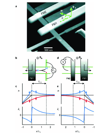
It is natural to expect that, if a charge-current induces a transverse spin-imbalance through the spin-orbit interaction, a spin-current will induce a transverse charge-imbalance (and a measurable voltage) by the same mechanismhirsch . In our experiments (Fig. 1a), a ferromagnetic electrode (FM1) is used to inject spin-polarized electrons via a tunnel barrier in one of the arms of an aluminum (Al) Hall cross. As shown in Fig. 1b, the injected current is driven away from the Hall cross, where only a pure spin-current flows as a result of the spin injection. If spin-orbit scattering is present, the spin-current could induce a transverse spin-Hall charge imbalance and generate a measurable voltage, . At a distance from the spin injector, the two transverse probes forming the Hall cross are used to measure such a voltage. The tunnel barriervanwees1 is important because it assures a uniformly distributed injection current, and enhances the polarization of the injected electronsSOV1 ; SOV2 . The non-local nature of our measurement scheme eliminates spurious effects due to AMR in the FM electrode or the anomalous and standard Hall effects. As no net charge-current flows into the Hall cross, the direct generation of voltage by the standard Hall effect is precluded. Located at a distance from FM1 is a second ferromagnetic electrode (labelled FM2 in Fig. 1a) that is used for sample characterization, as explained below.
We prepare the devices with electron beam lithography and a two-angle shadow-mask evaporation technique to produce tunnel barriers in situ. The Al cross, with arms 400 nm and 60 nm wide, is first deposited at normal incidence onto a Si/SiO2 substrate using electron beam evaporation. Next, the Al is oxidized in pure oxygen (150 mTorr for 40 min) to generate insulating Al2O3 barriers. After the vacuum is recovered, the two FM electrodes (400 and 250 nm wide, and 50 nm thick) are deposited under an angle of 50∘, measured from the normal to the substrate surface. The FM electrodes form tunnel junctions where they overlap with the Al strip with a typical tunnel resistance of 4 k for FM1 and 6.5 k for FM2. For the FM electrodes, we use CoFe (80 wt. % Co), which provides a large polarization when combined with Al2O3 as a tunneling barrierSOV1 ; douwe . The difference in the FM electrodes widths is required to get different coercive fields. A crucial point in our fabrication procedure is that no image of the Hall cross is deposited during the evaporation of FM1 and FM2, as observed in the atomic force micrograph of Fig. 1a. The FM deposits on the wall of the lithography mask and it is removed by lift-off, preventing unwanted short circuits (see Ref. SOV1, and Supplementary Information, Fig. 1).
The spin polarization of the electrons injected by FM1 depends on the effective tunnel conductances for spin-up and spin-down electrons, and , and can be written as . The spin-polarized current causes unequal electrochemical potentials for the spin up and down populations in Al (Fig 1c, top panel) and a spin current which flows to both sides of the contact and decays with the spin diffusion length, (Fig. 1c, bottom panel). As a result, the charge imbalance that is built up at the edges of the Al strip, and are expected to be proportional to and to decay with . Their magnitude is determined by the anomalous Hall operatorzhang1 ; bra1 ; bra2 ; zhang2 , , where denotes the spin Hall conductivity, is the spin index, and is an effective spin-dependent “electric” field, which follows from the spin-dependent electrochemical potential along the Al strip, i.e. .
Spin imbalance in the Al film occurs with a defined spin direction given by the magnetization orientation of the FM electrode. Consequently, is expected to vary when a magnetic field perpendicular to the substrate, , is applied and the magnetization of the electrode is tilted out of the substrate plane. Defining as the angle between and the electrode axis (Fig. 1a), we see, from the cross product in the anomalous Hall operator, that is proportional to , correlating with the component of normal to the substrate. As discussed below, can be set to be any value between and degrees with 2T.
We first characterize the properties of our device. FM1 and FM2, together with the Al strip, define a reference Johnson and Silsbee spin-transistorjs1 ; js2 ; js3 with Jedema et al. thin-film layoutvanwees1 . We use this spin-transistor to obtain , , and at . Measurements are performed at 4.2 K as represented in Figs. 1d and 1e (note the change in the direction of in Figs. 1d and 1b). Both and are obtained by measuring the spin transresistance as a function of , where is the difference in the output voltage between parallel and antiparallel magnetization configurations of the FM electrodes at zero magnetic fieldvanwees1 ; js1 ; js2 ; js3 ; alex ; havi . A lock-in amplifier is used with equal to 50 A. At larger currents, a marked decrease in the spin polarization is observed, as previously reportedSOV2 .
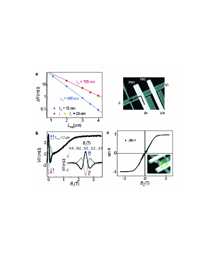
Figure 2a shows results for three different batches of samples with different Al thickness, . As noted recentlySOV1 , in Al films is strongly dependent on . We use this property to study the SHE in Al with different . The top two sets of measurements correspond to nm (red circles and green diamonds), whereas the bottom one (blue squares) corresponds to nm. The data shown in red and green are almost identical, demonstrating the high reproducibility of our sample fabrication. By fitting the data tovanwees1 ; js1 ; js2 ; js3 ; alex , where is the Al conductivity [; ] and the cross sectional area of the Al strip, we obtain , nm, and nm.
The tilting angle can be obtained from the spin precession results shown in Fig. 2b, which are measured with between -3.5 to 3.5 T. For small , the magnetizations of the FM electrodes remain in plane due to shape anisotropy, and the measurements show the Hanle effect associated with precessing spins. As increases, the magnetizations tilt out of plane. For large enough , they orient completely along the field and the measurements saturate to a positive constant value. The output voltage normalized by its value, , at has the form , for initially parallel (+) and antiparallel (-) configurations of the magnetizations, with a given function of vanwees1 ; js2 ; js3 . By noting that , is eliminated, and the calculation of is straightforward. The result of this calculation is presented in Fig. 2c. At , due to shape anisotropy. When is applied, the magnetization follows the Stoner-Wohlfarth modelohan with a saturation field of about 1.55 T for which approaches one, and the magnetization aligns with the field.
Having determined , and , we study the SHE using the measurement configuration shown in Fig. 1b. A change in results in a change in . By considering the spin diffusion using a semiclassical Boltzmann approximation, the spin Hall resistance at (see Fig.1b) can be calculatedzhang1 ; zhang3 :
| (1) |
with
| (2) |
Here it is assumed that the distance between the two voltage probes (Al strip width) is smaller than . in equation (2) was obtained by Zhang (see Refs. zhang1, and zhang3, ). The factors and in equation (1) account for the orientation of the spins and the fact that they diffuse away from FM1 into two (Al) branches instead of one, as in Ref. zhang3, . Note that, in the present configuration, the measurements are not affected by spin-precession because the component of the spins perpendicular to the substrate (or the transverse component of the anomalous velocity) is not modified by this effect.
Figure 3 shows as a function of for samples with = 860, 590, and 480 nm (circles) and nm. The sign convention is shown in the inset, where a positive is pointing out of the page. is swept between -3.5 and 3.5 T. We observe a linear response around , followed by a saturation on the scale of , both for positive and negative . Similar results were obtained in about 20 samples with different .
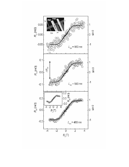
The saturation in for strongly suggests that the device output is related to the magnetization orientation of the FM electrode (see Fig. 2c) and the spin-Hall effect. This idea is further reinforced by comparing with the magnetization component perpendicular to the substrate, which as discussed above is proportional to (lines in Fig. 3). The agreement is excellent; the proportionality between and in equation (1) is closely followed.
For smaller than , a small linear term in becomes apparent (see bottom panel of Fig. 3 and inset). We believe that this term arises from the contribution of the orbital Lorentz force to the spin-Hall induced charge currentbra2 , which is a second-order effect that decays faster with than the spin Hall voltage itself.
Measurements were again performed with equal to 50 A. Larger currents lead to a decrease in as the voltage drop at the tunnel junction increases. This correlates with the decrease in the spin polarization observed with the spin-transistor measurementsSOV2 and further supports the interpretation of our results as being spin-related.
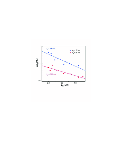
Consistent with equation (2), the overall change of , , decreases as a function of (Fig. 3). By fitting the magnetic field dependence of in Fig. 3 to equation (1), we have obtained for each sample. The results are shown in Fig. 4 as a function of , which are then fitted to equation (2) in order to obtain and . We find (12 nm) = nm, and (25 nm) = nm, in good agreement with the values obtained independently with the control spin-transistor (Fig. 2a). By using , we find (12 nm) = ( m)-1 and (25 nm) = ( m)-1. The ratio 1-3 is of the same order of magnitude as the one obtained experimentallyaws1 and theoreticallybert ; tse for GaAs. The predicted , when considering -like scattering centers, is zhang1 ; bra1 , where is Planck’s constant divided by , states/eV m3 is the density of states of Al at the Fermi energy pap , is the dimensionless spin-orbit coupling constant of Al bra2 , and and are the charge and mass of the electron. Without free parameters, we obtain ( m)-1 and 0.4-1 , in reasonable agreement with the experimental results.
We have thus presented electrical measurements of the spin-Hall effect in a diffusive metallic conductor (aluminum), and have obtained the spin-Hall conductivity. We have studied spin injection and spin relaxation with both reference spin-transistors and spin Hall crosses, obtaining consistent results.
This work demonstrates new means to study spin-related phenomena. It shows that the spin Hall effect can be used to directly measure spin polarized currents without the need of ferromagnets. Spin precession does not modify the spin Hall voltage for magnetic fields perpendicular to the substrate, as in the configuration discussed here. However, preliminary measurements with a magnetic field applied parallel to the Al strip suggest the generation of a spin Hall voltage that is a consequence of out-of-plane spins induced by spin precession.
References
- (1)
- (2) Wolf, S.A. et al. Spintronics: a spin-based electronics vision for the future. Science 294, 1488-1495 (2001).
- (3) Dyakonov, M.I., & Perel, V.I. Possibility of orienting electron spins with current. JETP Lett. 13, 467-469 (1971).
- (4) Dyakonov, M.I., & Perel, V.I. Current-induced spin orientation of electrons in semiconductors. Phys. Lett. A 35, 459-460 (1971).
- (5) Hirsch, J.E. Spin Hall effect. Phys. Rev. Lett. 83, 1834-1837 (1999).
- (6) Kato, Y.K., Myers, R.C., Gossard, A.C. & Awschalom, D.D. Observation of the spin Hall effect in semiconductors. Science 306, 1910-1913 (2004).
- (7) Wunderlich, J., Kaestner, B., Sinova, J., & Jungwirth, T. Experimental observation of the spin Hall effect in a two-dimensional spin-orbit coupled semiconductor system. Phys. Rev. Lett. 94, 047204 (2005).
- (8) Sih, V., Myers, R.C., Kato, Y.K., Lau, W.H., Gossard, A.C. & Awschalom, D.D. Spatial imaging of the spin Hall effect and current-induced polarization in two-dimentional electron gases. Nature Physics 1, 31-35 (2005).
- (9) Zhang, S. Spin Hall effect in the presence of spin diffusion. Phys. Rev. Lett. 85, 393-396 (2000).
- (10) Murakami, S., Nagaosa, N. & Zhang, S.C. Dissipationless quantum spin current at room temperature. Science 301, 1348-1351 (2003).
- (11) Sinova, J., Culcer, D., Niu, Q., Sinitsyn, N.A., Jungwirth, T. & MacDonald, A.H. Universal intrinsic spin Hall effect. Phys. Rev. Lett. 92, 126603 (2004).
- (12) Shchelushkin, R.V. & Brataas, A. Spin Hall effects in diffusive normal metals. Phys. Rev. B 71, 045123 (2005).
- (13) Shchelushkin, R.V. & Brataas, A. Spin Hall effect, Hall effect, and spin precession in diffusive normal metals. Phys. Rev. B 72, 073110 (2005).
- (14) Jedema, F.J., Heersche, H.B., Filip, A.T. Baselmans, J.J.A. & van Wees, B.J. Electrical detection of spin precession in a metallic spin valve. Nature 416, 713-716 (2002).
- (15) Valenzuela, S.O. & Tinkham, M. Spin-polarized tunneling in room-temperature spin valves. Appl. Phys. Lett. 85, 5914-5916 (2004).
- (16) Valenzuela, S.O., Monsma, D.J., Marcus, C.M., Narayanamurti, V. & Tinkham, M. Spin polarized tunneling at finite bias. Phys. Rev. Lett. 94, 196601 (2005).
- (17) Monsma, D.J. & Parkin, S.S.P. Spin polarization of tunneling current from ferromagnet/Al2O3 interfaces using copper-doped aluminum superconducting films. Appl. Phys. Lett. 77, 720-722 (2000).
- (18) Qi, Y. & Zhang, S. Spin diffusion at finite electric and magnetic fields. Phys. Rev. B 67, 052407 (2003).
- (19) Johnson, M. & Silsbee, R.H. Interfacial charge-spin coupling: injection and detection of spin magnetization in metals. Phys. Rev. Lett. 55, 1790-1793 (1985).
- (20) Johnson, M. & Silsbee, R.H. Coupling of electronic charge and spin at a ferromagnetic-paramagnetic metal interface. Phys. Rev. B37, 5312-5325 (1988).
- (21) Johnson, M. & Silsbee, R.H. Spin injection experiment. Phys. Rev. B37, 5326-5335 (1988).
- (22) Ji, Y., Hoffmann, A., Jiang, J.S. & Bader, S.D. Spin injection, diffusion, and detection in lateral spin-valves. Appl. Phys. Lett. 85, 6218-6220 (2004).
- (23) Urech, M., Korenivski, V., Poli, N. & Haviland, D.B. Direct demonstration of decoupling of spin and charge currents in nanostructures. Nano Letters 6, 871-874 (2006).
- (24) O’Handley R.C. Modern magnetic materials. (John Wiley & Sons, New York, 2000).
- (25) Zhang, S. Probing spin currents in semiconductors. J. Appl. Phys. 89, 7564-7566 (2001).
- (26) Engel, H.A., Halperin, B.I. & Rashba, E.I. Theory of spin Hall conductivity in n-doped GaAs. Phys. Rev. Lett. . 95, 166605 (2005).
- (27) Tse, W.K. & Das Sarma, S. Spin Hall effect in doped semiconductor structures. Phys. Rev. Lett. . 96, 056601 (2006).
- (28) Papaconstantopoulos, D.A. Handbook of the Band Structure of Elemental Solids (Plenum, New York, 1986).
*Present address: Francis Bitter Magnet Laboratory, Massachusetts Institute of Technology, Cambridge, MA 02139, USA
Supplementary Information is linked to the online version of the paper at www.nature.com/nature.
Acknowledgments We thank L. DiCarlo, H.A. Engel, D.J. Monsma and W.D. Oliver for a critical reading of the manuscript. This research was supported in part by the US National Science Foundation and the US Office of Naval Research.
Author Information Correspondence and request for materials should be addressed to S.O.V. (sov@mit.edu).