Realization of arbitrary single-qubit gates through control of spin-orbit couplings in semiconductor nanowires
Abstract
We propose a theoretical scheme to realize arbitrary single-qubit gates through two simple device units: one-dimensional semiconductor wires with Dresselhaus spin-orbit coupling (SOC) and Rashba SOC, separately. Qubit information coded by the electron spin can be accurately manipulated by the SOC when crossing the semiconductor wire. The different manipulative behaviors in Dresselhaus and Rashba wires enable us to make the diverse quantum logic gates. Furthermore, by connecting the Dresselhaus and Rashba units in series, we obtain a universal set of single qubit gates: Hadamard, phase, and gates, inferring that an arbitrary single qubit gate can be achieved. Because the total transmission is satisfied in the two device units, all the logic gates we have obtained are lossless. In addition, a ballistic spintronic switch is proposed in the present investigation.
PACS Numbers: 71.70.Ej, 85.35.Be, 03.67.-a
Quantum logic gate is the basic building block of quantum computer, which has attracted considerable attention recently. A variety of physical implementations have been proposed to realize the quantum gates Nielsen ; Yamamoto ; Step , among them the solid-state (especially nanoelectronic) implementations, are regarded to be one of the most suitable candidates to realize truly large-scale quantum computer in reality. Meanwhile, the qubit information coded by the spin degrees of freedom in solid-state system, is believed to be much more robust and stable than charge qubit, for having relatively long coherence time Kane ; Band . Based on these two considerations, a large class of spin-based logic gate schemes have been proposed in semicondutor nanostructures, mainly in semiconductor quantum dots Step ; Band ; Loss . The one and only exception is the scheme presented by Földi et al Foldi , who first concretely designed the spintronic single-qubit gates using one-dimensional semiconductor rings, based on the fact that the precession of the eletron spin can be accurately manipulated by the Rashba spin-orbit coupling (SOC) Rashba without the requirement of external magnetic field Datta ; Mire . It is thus feasible in principle to carry out all-electrical quantum computation in future Popescu . However, the functions of the logic gates they proposed were tuned a little bit complicated by changing both the external electric field and the geometries of the units. That is, in addition to the relatively easy tuning of Rashba SOC by electric field, several rings with different sizes and different geometry angles must be fabricated, which greatly reduces the flexibility and unitary of the device assemble.
Except the Rashba interaction, there is another typical SOC, i.e. Dresselhauls SOC Dresselhaus exiting in the semiconductor sample, which appears as a result of bulk Dresselhaus and interface Dyak inversion asymmetries. Its strength had been considered not to be tuned as conveniently as that of Rashba interaction. Recent theoretical Wu and experimental Kato2 work showed the Dresselhaus spin splitting could be effectively adjusted via strain existing in the structure. Schliemann and Loss Schliemann predicted that the Dresselhaus coefficient in a quantum well might also be conveniently altered by an electric field. Therefore, it is possible to carry out practical ways in experiments to control the strength of Dresselhaus interaction.
In the present work, we propose a theoretical scheme to implement a universal set of single-qubit gates in semiconductor nanowires, based on both Rashba and Dresselhaus SOCs. The basic device units are two quasi-one-dimensional electron gas (1DEG) systems with either Dresselhaus or Rashba SOC, sandwiched between two leads. We find both the Dresselhaus and Rashba units can serve as lossless quantum gates, but the properties of the gates are different resulting from the different SOC mechanisms. By connecting the two device units in series, a universal set of single-qubit gates: Hadamard, phase, gates Nielsen , can be implemented, inferring an arbitrary single qubit gate can be obtained in our scheme. The important arbitrary phase gate Nielsen can be obtained by tuning the strength of Dresselhaus interaction, which can greatly optimize the circuits when building quantum computer. In addition, a ballistic spintronic switch is suggested.
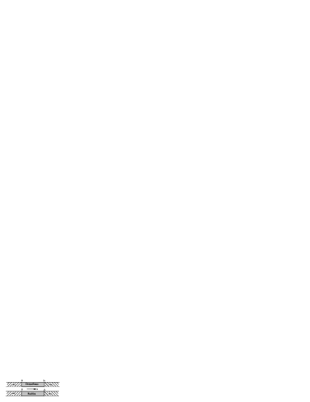
Figure 1 shows the schematics of the two device units: Dresselhaus-type (above) and Rashba-type nanowires (below). When the cross-section of the nanowire is sufficiently small, only electronic motion in the longitudinal direction is of interest, i.e., the system becomes quasi-one-dimensional note1 . The SOC region along direction is sandwiched between two leads. An electron wave is injected from the left lead to the right one crossing the middle SOC region. The Schrödinger equations in the three regions are solved separately. The Hamiltonians in the Dresselhaus- and Rashba-type nanowires can be respectively described by
| (1) | |||||
| (2) |
where is the effective mass of electrons and are the Pauli matrices. The coefficients and express the Dresselhaus and Rashba strengths, respectively. We choose in leads, and in the middle SOC region. To model the elastic scattering that usually occurs at the two interfaces between the leads and the SOC region, we follow the previous work to include a -function potential with the height of , at positions of and Blonder ; Matsuyama . The parameters and indicate the lengths of the Dresselhasu and Rashba regions, respectively. A dimensionless parameter is introduced to represent the strength of the interfacial scattering, where is the incident electron energy. No spin-flip across the interfaces is assumed in the calculation Blonder ; Matsuyama .
The wave functions in the left (source) and right (drain) leads can be written as and respectively, where is the wave vector in the leads. The spinors , , and respectively represent the spin states of the incident, reflective, and transmission waves. The coefficients are arbitrary complex numbers and satisfy . If the two coefficients and in the reflective wave are known, the reflective probability can be obtained through The spin state becomes after being tuned by the middle SOC interaction. The transmission coefficient of the outgoing wave can be obtained from According to the conservation of the particle number, is guaranteed in all the calculations.
The degenerate up- and down-spin states at in electrodes (corresponding to the incident energy ) will lift into four different wave vectors and in the middle region due to the SOC interaction. Therefore, the up- and down-spin wave functions in the middle SOC region can be expanded with the four corresponding eigenspinors. The wave function in this region can be expressed as At a fixed , the coefficient is related to by the eigenspinors for infinite SOC system. It is found that for the two kinds of SOCs, the eigenspinors for the infinite systems are different. There are four independent coefficients to be determined in the SOC region. They together with another four coefficients in the two leads ( ) can be solved by boundary conditions at the two interfaces normal to direction Yao . After the equations are solved, we can get the spin states of outgoing wave and establish the relations between the incoming and the outgoing spin states by introducing a transformation matrix :
| (3) |
In Dresselhaus device, , and in Rashba one, , where and are unitary and unimodular matrices, describing the spin transformation properties in Dresselhaus and Rashba units, respectively. A possible global phase in the form of can be neglected in and , since the effect of the global phase is not observable in quantum computation Nielsen . To attain lossless qubit gates, the complete transmission () must be satisfied.
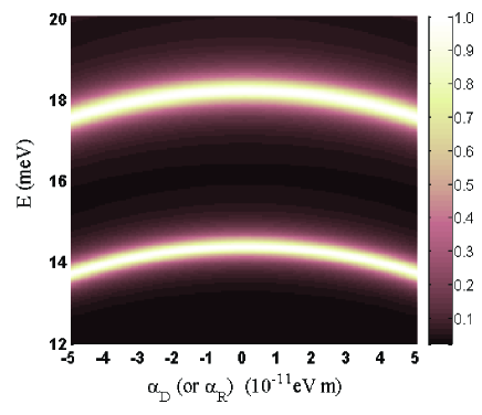
In the calculation, the effective mass is set as . The lengths of the SOC regions and , fixed at nm, are restricted within ballistic region, i.e., and are smaller than the phase-coherent length , which is in the range of 0.4-1.0 m Nitta ; Nomura ; Souma ). Ballistic samples with small dimensions are always desirable for future electronic device applications. Fig. 2 shows the transmission coefficient for the Dresselhaus and Rashba units, in which a moderate -potential is considered. Here we note that if the corresponding parameters of these two geometries are of the same values, the totally same results of the transmission are obtained, which can be ascribed to the same phase interference properties between the four waves in the two kinds of SOC regions. Two bright camber areas corresponding to are clearly seen, within which the geometry can serve as a lossless single-qubit gate. The energy width corresponding to the total transmission is about meV (see the upper camber). It decreases a little bit in the lower camber. This behavior shows that the bias applied on the wires should be in linear region and within the magnitude of meV to build the lossless qubit gates. Between the two total transmission regions, there is a wide energy gap, in which the transmission coefficient is too small to devise the logic gates.
Except the SOC strength and the incident energy, the height of the potential at the two interfaces also significantly influences the transmission of the electron. Figure 3 provides the transmission coefficient as a function of the SOC strength ( or ) under various magnitudes of potential, where the incident energy is fixed at meV. When , the total transmission can only occur at certain potential height . If deviates from (either larger or smaller), the transmission decreases, indicating that the resonant-like transmission occurs between the two potentials with the height of . When the potential barrier is fixed at , the total transmission is obtained in a wide range of Rashba strength, which means a great number of logic gates can be realized there. Increasing the height of the potential, two narrower peaks corresponding to appear. In practice case, we certainly hope to find the situation corresponding to the solid curve.

The spin transformation properties in Dresselhaus and Rashba device units are found to be different: , , where the parameters and . They express the rotation angles of spinors of electrons after crossing the spin-orbital coupling regions. It is reasonable that the rotation angle is proportional to the strength of the SOC and the length of the SOC regionMire .
Various qubit gates can be realized by the above two device units. Clearly, the non-trivial NOT gate Nielsen can be implemented through Dresselhaus device unit, if is satisfied at the base of . For example, if the Dresselhaus device parameters are set as: nm, meV, , the NOT gate can be approximately obtained when eVm. Besides the NOT gate, another two unitary matrices and can be realized in Dresselhaus device by tuning the value of , and will play a critical role in devising the important phase and gates, which will be discussed in details later .
For Rashba device unit, if the spin rotation angle and , we can obtain the transformation matrix of . This is a pseudo-Hadamard gate because it lacks the correct determinant of genuine Hadamard. The similar conclusion has also been drawn in quantum Rashba-type ring Foldi . If the Rashba device are modeled with the parameters: nm, meV, and , the pseudo-Hadamard can be attained when is fixed at eV m. Tuning to let , we get the pseudo-NOT gate . In addition, we find the identity matrix can be realized with the condition of . This means that the Rashba effect can be totally ’cancelled’ and the electrons can reach the right lead with its original spin state unchanged.
The product of the pseudo-NOT gate and the NOT gate gives the Z gate . This means that the Z qubit gate can be implemented by connecting in series one Rashba device unit with one Dresselhaus unit. Similarly, the genuine Hadamard gate Nielsen can be achieved by connecting the pseudo-Hadamard gate (made from the Rashba unit) with the NOT gate (made from the Dresselhaus unit). We find the phase gate and the gate can be decomposed as: and ( stands for the Hadamard gate), respectively. This means that both of them can be realized by connecting three Dresselhaus and two Rashba device units in series with certain sequence. The Hadamard, phase, and gates constitute a universal set of single-logic gates, based on which any single quantum gates can be built to arbitrary precision Nielsen . A continuous phase gate Nielsen , decomposed as , is actually implemented by just varying the Dresselhaus strength. This is a superior character compared with the previous work Foldi , in which the phase gate is tuned by changing the geometry angle.
In addition, from Fig. 3, we find that a ballistic spintronic switch can be made by the Rashba device unit. The near complete transmission at certain values of corresponds to the “ON” of the switch. The near-zero transmission is regared as “OFF”. Therefore, by tuning the gate voltage Nitta , we can easily control the device to be “ON” or “OFF”. Since the sample size is in the ballistic region with the length of nm, it may be used in future nano-sized electronic devices.
In conclusion, a theoretical scheme is presented for realization of arbitrary single-qubit gates based on two quasi-one-dimensional semiconductor wires with Dresselhaus and Rashba interactions, separetely. All the single-qubit gates would be realized possibly by using a series of semiconductor nanowires with the same geometry and lead connection, which simplifies the device manufacturing and is in favor of large scale integration. In addition, a ballistic spintronic switch is proposed, whose “ON” and “OFF” can be tuned conveniently by varying external electric field.
The authors are grateful to Prof. X. Wang in Fudan Univ. for very helpful discussion. This work was supported by the National Natural Science Foundation of China with grant No.10304002, the Grand Foundation of Shanghai Science and Technology (05DJ14003), PCSIRT, and the Fudan High-end Computing Center.
References
- (1) E-mail address: zyang@fudan.edu.cn.
- (2) M. A. Nielsen and I. L. Chuang, Quantum Commputation and Quantum Information, Cambridge University Press, Cambridge (2000).
- (3) T. Yamamoto, Yu. A. Pashkin, O. Astafiev, Y. Nakamura and J. S. Tsai, Nature 425, 941 (2003).
- (4) D. Stepanenko and N. E. Bonesteel, Phys. Rev. Lett. 93, 140501 (2004).
- (5) B. E. Kane, Nature 393, 133 (1998).
- (6) S. Bandyopadhyay, Phys. Rev. B 61, 13813 (2000).
- (7) D. Loss and D. P. Divincenzo, Phys. Rev. A 57, 120 (1998).
- (8) P. Földi, B. Molnár, M. G. Benedict, and F.M. Peeters, Phys. Rev. B 71, 033309 (2005).
- (9) Y. A. Bychkov and E. I. Rashba, J. Phys. C 17, 6039 (1984).
- (10) S. Datta and B. Das, Appl. Phys. Lett. 56, 665 (1990).
- (11) F. Mireles and G. Kirczenow, Phys. Rev. B 64, 024424 (2001)
- (12) A. E. Popescu and R. Ionicioiu, Phys. Rev. B 69, 245422 (2004).
- (13) G. Dresselhaus, Phys. Rev. 100, 580 (1955).
- (14) M. I. Dyakonov and V. Y. Kachorovskii, Sov. Phys. Semicond. 20, 110 (1986).
- (15) L. Jiang and M. W. Wu, Phys. Rev. B 72, 033311 (2005).
- (16) Y. K. Kato, R. C. Myers, A. C. Gossard, and D. D. Awschalom, Phys. Rev. Lett. 93, 176601 (2004).
- (17) J. Schliemann and D. Loss, Phys. Rev. B 68, 165311 (2003).
- (18) For example, the model can describe well a quasi-1DEG system with width less than 20 nm, since the first confinement energy of the geometry is found to be higer than 20 meV and the Fermi energy of a semiconductor 2DEG is generally about or below 20 meV.
- (19) G.E. Blonder, M. Tinkham, and T.M. Klapwijk, Phys. Rev. B 25, 4515 (1982).
- (20) T. Matsuyama, C.-M. Hu, D. Grundler, G. Meier, and U. Merkt, Phys. Rev. B 65, 155322 (2002); C.-M. Hu, T. Matsuyama, Phys. Rev. Lett. 87, 066803 (2001).
- (21) J. Yao and Z. Q. Yang, Phys. Rev. B 73, 033314 (2006).
- (22) J. Nitta, T. Akazaki, H. Takayanagi, and T. Enoki, Phys. Rev. Lett. 78, 1335 (1997).
- (23) K. Nomura, J. Sinova, T. Jungwirth, Q. Niu, and A. H. Macdonald, Phys. Rev. B 71, 041304 (2005).
- (24) S. Souma and B. K. Nikolić, Phys. Rev. Lett. 94, 106602 (2005).