Inelastic tunneling effects on noise properties of molecular junctions
Abstract
The effect of electron-phonon coupling on the current noise in a molecular junction is investigated within a simple model. The model comprises a 1-level bridge representing a molecular level that connects between two free electron reservoirs and is coupled to a vibrational degree of freedom representing a molecular vibrational mode. The latter in turn is coupled to a phonon bath that represents the thermal environment. We focus on the zero frequency noise spectrum and study the changes in its behavior under weak and strong electron-phonon interactions. In the weak coupling regime we find that the noise amplitude can increase or decrease as a result of opening of an inelastic channel, depending on distance from resonance and on junction asymmetry. In particular the relative Fano factor decreases with increasing off resonance distance and junction asymmetry. For resonant inelastic tunneling with strong electron-phonon coupling the differential noise spectrum can show phonon sidebands in addition to a central feature. Such sidebands can be observed when displaying the noise against the source-drain voltage, but not in noise vs. gate voltage plots obtained at low source-drain bias. A striking crossover of the central feature from double to single peak is found for increasing asymmetry in the molecule-leads coupling or increasing electron-phonon interaction. These variations provide a potential diagnostic tool. A possible use of noise data from scanning tunneling microscopy experiments for estimating the magnitude of the electron-phonon interaction on the bridge is proposed.
pacs:
72.70.+m 72.10.Di 73.63.-b 85.65.+hI Introduction
Development of molecular electronics as a complement to traditional semiconductor-based electronics provides challenges both experimentally and theoretically.MEB ; AN ; Reed ; Cuniberti ; Bowler Early studies of molecular junctions were restricted to measurement of current-voltage (or conductance-voltage) characteristics of such junctions and their dependence on junction parameters such as wire length, molecular structure, molecule-lead coupling, and temperature.lang ; kubiak ; reed_tour ; heath ; joachim ; weber More recently, charging (Coulomb blockade) and inelastic and mechanical effects appear at the forefront of research.park ; bjornholm ; mceuen ; natelson ; ho ; zhitenev In particular, inelastic electron tunneling spectroscopy (IETS) has become an important diagnostic and characterization tool, indicating the presence and structure of a molecule in the junctionho ; zhitenev and providing information on the junction structure.ruitenbeek
In addition to the behavior, noise characteristics can provide information about molecular junctions.noiserev_Buttiker Noise measurements in mesoscopic tunnel junctions have been under study for a long fine, e.g. in semiconductor double barrier resonant tunneling structures (DBRTS),e_DBRTS_Li ; e_DBRTS_Safonov ; e_DBRTS_Nauen ; e_DBRTS_Jung quantum point contacts (QPC),e_QPC_Li ; e_QPC_Washburn ; e_QPC_Liefrink ; e_QPC_Reznikov Coulomb blockaded Josephson junctions,e_JJ_Delahaye ; e_JJ_Lindell and advances in understanding their diagnostic capabilities are being made (see, e.g. e_3rdmoment_Reulet, ). Results of measurements in molecular tunnel junctions are expected to appear in the near future, though these measurements are difficult due to the background noise caused by charge fluctuations in the environment. Many theoretical studies of noise in nanojunction transport are available in the literature (see Ref. noiserev_Buttiker, and references therein). In particular noise in DBRTS was studied within the nonequilibrium Green function (NEGF) formalism in the ballistict_DBRTS_Chen ; t_DBRTS_Levy and the Coulomb blockadet_DBRTS_Hung ; t_DBRTS_Thielmann regimes. Noise in QPC was studied within NEGFt_QPC_Averin and kinetic equation approaches,t_QPC_Green while noise in Coulomb blockaded Josephson junctions was investigated within a phase correlation theory approach.t_JJ_Sonin2 NEGF was also applied to study shot noise in chain modelst_chain_Aghassi ; t_chain_Kinderman and disordered junctions.t_disordered_Gutman Shot noise for coherent electron transport in molecular devices was investigated within a scattering theory approach in a number of works.t_mol_Dallakyan ; t_mol_Walczak ; t_mol_DiVentra2 Inelastic effects in the noise spectrum were studied recently, first in connection with nanoelectromechanical systems (NEMS)t_NEMS_Nishiguchi ; t_NEMS_Smirnov ; t_NEMS_Clerk ; t_NEMS_Novotny ; t_NEMS_Flindt ; t_NEMS_Wabnig and ac-driven junctions.t_AC_Camalet ; t_AC_Guyon Substantial work on this issue has been done within a scattering theory approach.t_stmol_Shimizu ; t_stmol_Bo ; t_stmol_Dong ; t_stmol_DiVentra Finally predictions on phonon assisted resonant shot noise spectra of molecular junctions were obtained in Ref. noise_elph_Balatsky, within NEGF.
In this work we investigate inelastic tunneling and its influence on the zero frequency noise in a simple one-level molecular junction model. The one-level junction model focuses on one molecular orbital (say the lowest unoccupied molecular orbital, LUMO) that supports resonance transmission beyond a certain voltage bias threshold. The molecular orbital is coupled to a local oscillator representing the molecular nuclear subsystem. The oscillator in turn is coupled to a thermal harmonic bath. We have recently used this model within the NEGF methodology to study inelastic effects on electronic transport in molecular junctions in the weakIETS_SCBA and in the intermediate to strongstrong_el_ph electron phonon coupling regimes. Here we utilize the same approaches to investigate inelastic effects in the noise spectrum. The physics of the problem is determined by the relative magnitudes of the relevant energy parameters: - the spacing between the leads’ Fermi energies and the energy of the molecular orbital, - the broadening of the molecular level due to electron transfer interaction with the leads, - the electron-phonon coupling and - the phonon frequency. We consider both resonant and far off-resonant inelastic tunneling cases. In the off-resonant limit, it is usually the case that also and the process can be described in the weak electron-phonon coupling limit. For resonance transmission, , the electron-phonon interaction may still be weak, .weakM These weak coupling situations can be treated within standard diagrammatic perturbation theory on the Keldysh contour, see e.g. IETS_SCBA, . More interesting physics is observed in the case of strong electron-phonon interaction, , which we treat within the self-consistent NEGF scheme introduced in Ref. strong_el_ph, . In both limits we apply the corresponding approach to study effects of electron-phonon coupling on the zero-frequency noise and the Fano factor.
Our results are discussed in comparison with recent work on the effect of electron-phonon coupling on the noise properties of molecular junctions. In the weak coupling limit our result agree qualitatively with the scattering theory based treatment of Chen and Di Ventrat_stmol_DiVentra in the case of near resonance transmission in symmetric junctions. However, in contrast to Ref. t_stmol_DiVentra, that finds that the leading contribution to this effect is of order we find that this effect is of order . Also, different qualitative behavior is found in off-resonance situations and for resonance transmission through asymmetric junctions.
In the strong electron-phonon coupling limit we compare our result to that of Zhu and Balatskynoise_elph_Balatsky who treat this problem using the (essentially scattering theory) procedure of Lundin and McKenzie.Lundin Again we find some new qualitative effects that can not be obtained from the simpler approach.
Our analysis suggests the usefulness of the “noise spectroscopy”, either in a source-drain response or in a gate voltage response, to measure the values of the electron-vibration coupling on the bridging molecule and to characterize the asymmetry in the coupling between the molecule and the source and drain electrodes.
Section II describes formal derivation of the expression for the noise through a molecular junction. In Section III we introduce the model. Section IV briefly reviews the noise properties of the elastic current. Section V sketches a procedure and presents numerical results for the case of weak electron-phonon coupling and Section VI does the same for the strong coupling case. Section VII concludes.
II General noise expression
A general expression for the frequency dependent noise in a 2-terminal junction can be obtained by applying the method of Meir and Wingreen. In its most general formulation this method assumes a single electron exchange between bridge and leads and invokes the non-crossing approximation (NCA)Bickers for the bridge-leads coupling. The system is described by the Hamiltonian
| (1) |
where , and denote the Hamiltonian of the independent molecule and the left and right leads, respectively and where () and () denote single electron annihilation (creation) operators in molecule and leads. The current operators for the molecule and each lead are defined by
| (2) |
and the average steady state current for a given potential bias is obtained in the formcurrent ; HaugJauho
| (3) | |||||
| (4) |
where are lesser/greater projections of the self-energy due to coupling to the (metallic) contact () and are lesser/greater Green functions, all these are defined in a molecular subspace of the problem. Obviously in steady state.
The noise spectrum is defined as the Fourier transform of the current-current correlation function. The relevant current fluctuations have to be considered carefully because by their nature such fluctuations correspond to transient deviations from steady states. We follow the analysis of Ref. Galperin, that leads to the following expression for the operator that corresponds to the current in the outer circuit
| (5) |
where
| (6) |
and are junction capacitance parameters that take into account the charge accumulation at the corresponding bridge-lead interface. Note that at steady state . The different signs assigned to and stem from the fact that the current is considered positive on either side when carriers enter the system (molecule).
In terms of , Eq. (5), the noise spectrum is defined by
| (7) | |||||
| (8) |
where and where the averaging is done as usual (and as in Eq. (3)) on the non-interacting state of the system at the infinite past. The same approachcurrent ; HaugJauho that leads to Eq. (3) now leads to the following general expression for the noise
| (9) | ||||
A similar approach was used by Bo and Galperinnoise_Galperin to obtain an expression analogous to (II) for a single level bridge model.noise_expression In this paper we restrict our consideration to the case of zero frequency noise which is the relevant observable when the measurement time is long relative to the electron transfer time, a common situation in usual experimental setup. Then the expression simplifies to
| (10) |
where with given by Eq. (4).
III The single level bridge/free electron leads model
Eq. (10) can be applied, under the approximations specified to very general bridge and leads models. Further progress can be made by specifying to simpler models. As usual we assume that the contacts are treated as reservoirs of free electrons, each in its own equilibrium. The molecule is described by the simplest coupled electron-phonon system as follows. Assuming that the energy gap between the orbitals relevant for a molecular junction (in particular the HOMO-LUMO gap) is much greater than level broadening due to coupling to the contacts, we consider the electron current through each orbital separately. Thus the molecular junction is represented by a single level (molecular orbital) coupled to two contacts ( and ). The electrons on the bridge are coupled to a local normal mode (henceforth referred to as primary phonon) represented by a harmonic oscillator. This is coupled to a thermal bath described by a set of independent harmonic oscillators (“secondary phonons”). The Hamiltonian is thus given by
| (11) |
where () are creation (destruction) operators of electrons on the level, () are the corresponding operators for electronic states in the contacts, () are creation (destruction) operators for the primary phonon, and () are corresponding operators for phonon states in thermal (phonon) bath. and are shift operators
| (12) |
Detailed discussion of the model and our self-consistent calculation procedures are presented in Refs. IETS_SCBA, and strong_el_ph, for weak and strong electron-phonon couplings respectively. Sections V and VI below provide brief outlines of these procedures.
In both weak and strong coupling cases the calculation is aimed to obtain the electron Green function (or rather its Langreth projectionsLangreth on the real time axis). Those Green functions are used for the calculation of the steady-state current across the junction (3) and the noise spectrum (10). The general current and noise expression remain as before, Eqs. (3), (II) and (10) (excluding the trace operations). The lesser and greater self-energies associated with the bridge-contact coupling are now given by
| (13) | |||||
| (14) |
with the Fermi distribution in the contact and
| (15) |
In the calculation described below we adopt the wide band approximation in which is assumed constant. In this approximation =.
The observed conduction and noise properties of our system depend on parameters that can not be accounted for by the present single-electron level of treatment. The capacitances and that define the parameters and that enter the noise calculation belong to this group. We also use below the voltage division parameter that determines the voltage induced shifts in the leads’ electrochemical potentials and relative to according to
| (16) |
This parameter affects the way by which the externally imposed bias translates into the relative positioning of electronic energies.
In addition, consider the ratio
| (17) |
that represents the asymmetry in molecule-lead couplings (wide band limit is assumed here and below). This is an experimentally controlled parameter that can be changed, e.g. with tip-molecule distance in an STM configuration or by using thin insulating layers to separate molecule from leads.Ho ; Repp
The connection (if any) between the parameters , and () is obviously of great interest. An equivalent circuit model for a molecular (or nanodot) junctionGalperin ; Tinkham ; IngoldNazarov usually describes the junction as serially connected circuits. Assuming that at steady state charges and accumulate on the corresponding capacitors the steady state relationships imply that . These relations imply in turn that
| (18) |
This leaves two important parameters in the model. These however can, at least in principle be determined experimentally: The rates can be determined by optical experimentsSilbey and the potential distribution on a conducting junction can be probed as demonstrated in Ref. McEuen, . In the present paper we use to characterize the junction asymmetry and several arbitrary values of chosen to represent different possible manifestations of noise behavior.
In addition, in this paper we discuss two experimental manifestations of nanojunction transport. In the first, the source-drain voltage is kept small and fixed, , and the gate voltage is varied in order to move the molecular orbital energy in and out of resonance. In the second, the gate voltage is fixed, e.g. , and varies so that resonance conditions are usually achieved for . In the latter case we restrict our consideration to the case where the onset of resonance transmission is caused by crossing the LUMO for a positively biased junction, and disregard other possible scenarios such as the crossing the HOMO.muRHOMO In both cases taking provides better resolution of resonance features. Also, in the resonant tunneling situation it is convenient to consider the first derivatives of the current and noise with respect to voltage, and respectively, rather than and themselves.
IV Noise in elastic transport
Before discussing inelastic effects we briefly review the issue of noise in the elastic tunneling situation. In this case current, Eq.(3), reduces to the well known Landauer expression
| (19) |
while the zero frequency noise expression (10) reduces to a sum of thermal contribution, , due to thermal excitations in the contacts and shot noise term, , due to the discrete nature of the electron transportnoiserev_Buttiker
| (20) | |||||
with
| (23) |
Using Eq. (16) this leads to (with )
| (24) | ||||
| (25) |
Interestingly, these results do not depend on the capacitance ratios . These expressions can be further simplified in two cases: (a) When the source-drain voltage is varied we consider, as indicated above, the situation where the signal is dominated by the resonance associated with the crossing between and . In this case the terms involving in Eqs. (24) and (25) are disregarded. (b) When the gate voltage is varied at small the two terms on the r.h.s. of Eqs. (24) and (25) are essentially the same and can be combined together.
In these elastic transmission cases both experimental procedures discussed above give essentially the same information. Recall that conductance is a Lorentzian function of that peaks at the position of the resonance level, with a width (FWHM) related to the total escape rate . In contrast, the differential noise graph ( vs. ) depends on the asymmetry of the molecule coupling in the junction . itself is a Lorentzian function of , so vs. has the form of a Lorentzian derivative that vanishes at the level position and peaks at with peak/dip heights respectively.heightasym The contribution from the zero temperature shot noise, vs. , depends on the coupling asymmetry . A double peak structure appears when has three extrema as a function of . The condition for this to occur is
| (26) |
so that for it yields a two peak structure with peaks at and peak heights of (in units of ). This behavior of is associated with the transition from double-barrier resonance structure at moderate asymmetry to a single tunneling barrier for the strongly asymmetric case. vanishes when or and maximizes when . This leads to a two peak structure in symmetric and nearly symmetric double barrier resonance supporting tunnel junctions (DBRTS). When the asymmetry is stronger the noise profile has a single peak form with peak position at . in both cases is given by (in units of ), which is for symmetric coupling case ().
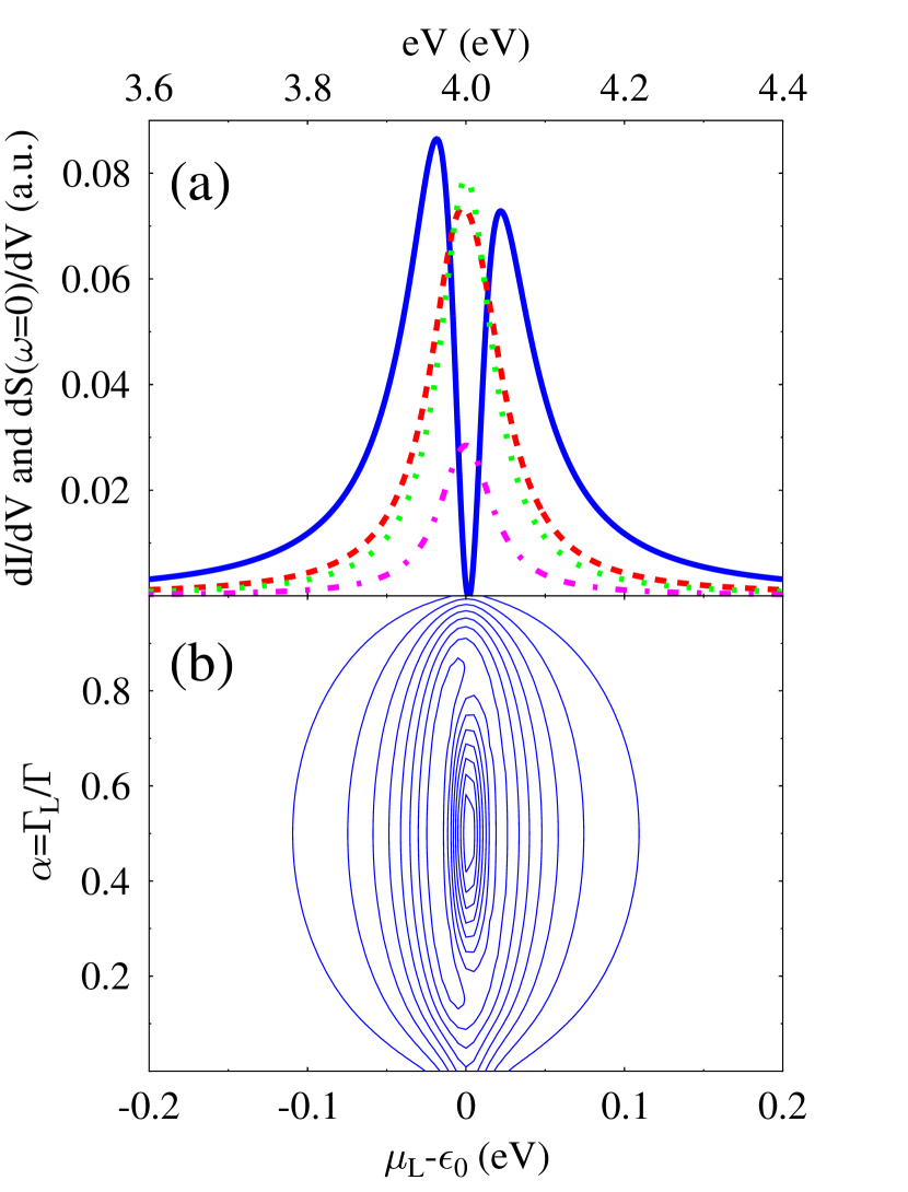
The sum determines the observed signal. Figure 1 illustrates the above discussion using the parameters eV, eV, and K. Here and below we use a.u. (atomic units) for current, noise and differential noise, , , and respectively, with the electron charge, the atomic unit of time, and the Planck constant. Fig. 1a shows plots of the conductance and the differential noise for symmetric () and strongly asymmetric () coupling. In both cases is a Lorentzian (dotted and dash-dotted lines respectively), while form of changes from a two-peak structure with complete noise suppression at for the symmetric case to a one peak structure in the asymmetric situation. Note that in the two-peak case the peak heights are different due to the thermal noise contribution. In principle both the peaks positions in the two-peak structure and the differential noise at may be used as sources of information on the asymmetry (expressed by the parameter ) in the molecule-leads couplings. A single peak shape indicates highly asymmetric coupling. Consequently, in STM experiments the shape of the differential noise vs. applied voltage plot will change when bringing the tip closer to the sample, decreasing the asymmetry.
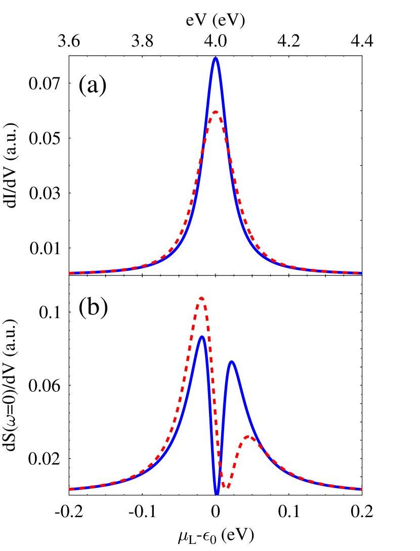
The effect of temperature is demonstrated in Fig. 2 where results for two temperatures, K and K respectively, are presented for the symmetric coupling case, . The differential conductance peak, as is expected, becomes wider and lower with increasing (Fig. 2a). At the same time the two peak structure of the differential noise plot becomes broader, and the difference in the peak heights of the two-peak structure in the differential noise plot becomes more pronounced (Fig. 2b).
V Weak electron-phonon coupling
We now turn to the model, Eq. (III), that includes the effect of electron-phonon interactions on the bridge. In this section we consider weak electron-phonon coupling which can be treated with the standard diagrammatic theory on the Keldysh contour. The lowest non-zero diagrams lead to the Born approximation (BA), while dressing of these diagrams yields its self-consistent version (SCBA). Detailed description of this approach and the derivation of the self-energies expressions can be found in our previous publication.IETS_SCBA Within the Born approximation the lesser and greater electron self-energies due to coupling to the local phonon can be expressed for the model at hand in terms of the (molecule projected) electron and phonon densities of states, and respectively, and of the electron and phonon energy-resolved occupations, and respectively,occ as follows (for details see Ref. IETS_SCBA, )
| (27) | ||||
| (28) | ||||
Note that in the 1-level bridge model employed here all the Green functions and self-energies are scalars defined in the bridge subspace. In the absence of electron-phonon coupling the densities of states are
| (29) | |||||
| (30) |
where , see Eq. (15), is resonant level escape rate due to coupling to the leads and is the local phonon decay rate due to coupling to the thermal bath. The phonon occupation in this limit is given by the Bose-Einstein distribution, , while the electron occupation in the junction is
| (31) |
where is Fermi-Dirac distribution of the contact . The electron relaxation rate due to coupling to the primary phonon is given by
| (32) |
The retarded electron self-energy due to this coupling is taken in what follows to be purely imaginary (tacitly assuming that its real part – level shift – has been incorporated into ), given by
| (33) |
Keeping terms up to the second order in the electron-phonon coupling we get for the electron Green functions
| (34) | ||||
| (35) | ||||
where
| (36) |
and where the lesser and greater electron self-energies due to coupling to contacts, , are given by Eqs. (13) and (14).
Using (13), (14), and (35) in (3) the average steady-state current through the junction is obtained in the form
| (37) |
where
| (38) |
with given in (23). The first term in parentheses in (38) yields usual Landauer expression, while the second gives the second order (in ) correction associated with the electron-phonon coupling. As discussed in Ref. IETS_SCBA, , this correction results from both the renormalization of the elastic transmission channel and the opening of the inelastic channel.
Using (13), (14), (34), (35) in (10) we get for the zero frequency noise
| (39) | ||||
where
| (40) | |||||
| (41) | |||||
| (42) |
One sees that in the presence of electron-phonon interaction the noise expression can not be separated into thermal and shot noise parts as is given by (20)-(IV).
Eqs. (37) and (V) are used in the calculations presented below. We will consider two limits of the electron tunneling process: 1. resonant, , and 2. off-resonant (superexchange), , where is the energy of the tunneling electron. The first situation was considered in Ref. t_stmol_DiVentra, . The second is a common situation in molecular junctions where the HOMO-LUMO gap is larger than both the orbital broadening and applied voltage. It was pointed out by us and others that since is negative (positive) in the resonant (non-resonant) situations the current change upon the onset of inelastic tunneling, , is negative in the resonant case and positive in the off-resonance limit.
Figure 3 presents the zero frequency noise , displayed against the applied voltage for the resonant tunneling case in (a) symmetric coupling, , and (b) strongly asymmetric coupling, , situations. Parameters of the calculation are K, eV, eV, , eV, eV, eV, and eV. The full and dashed lines in Fig. 3 correspond to the calculated noise in the presence and absence of electron-phonon interaction, respectively. The dotted line results from an attempted approximation in which the noise was computed from Eqs. (20)-(IV) except that was replaced by , Eq. (38). Two points are noteworthy here. First, opening of the inelastic channel, at , may lead both to increase (symmetric coupling, Fig. 3a) and decrease (asymmetric coupling, Fig. 3b) of the noise signal. Second, modifying Eqs. (20)-(IV) by replacing the bare transmission by the phonon-renormalized transmission shows a similar qualitative dependence of the noise on the electron-phonon interaction as our more rigorous results, but fails quantitatively (compare full and dotted lines in Fig. 3a).
While the calculations presented below are made with no additional assumptions, a valuable insight can be gained by considering the low temperature limit, , assuming and/or , and taking the voltage large enough so that the inelastic channel is open, . In this case and . Under these additional assumptions we obtain for the noise change upon the onset of inelastic tunneling (up to ) from (V) in the resonant tunneling situation
| (43) | ||||
| (44) |
Using (44) in (43) one can show that for symmetric coupling, , . This together with in the resonant tunneling case leads to (predicted in Ref. t_stmol_DiVentra, ) increase in Fano factor, , upon opening of the inelastic channel. The situation can be different however for asymmetric junctions. Indeed, Eqs. (43) and (44) imply that if the inequality
| (45) |
is satisfied the change in the zero frequency shot noise is negative, . In this case the Fano factor can decrease with the opening of inelastic channel.
Figures 4a and 4b (which were obtained, as already noted, without invoking these simplifying assumptions) validate these observations. Fig. 4a shows, for a symmetric junction a trend (smaller current, larger noise and consequently larger Fano factor in the presence of electron-phonon interaction) similar to that suggested by Chen and Di Ventrat_stmol_DiVentra (see Fig. 2 there). However the trend shown in Fig. 4b for the asymmetric junction is opposite. It should also be noticed that while the phonon induced change in the noise was obtained in t_stmol_DiVentra, to be of order , Eq. (43) shows contributions of order that dominate in the weak electron-phonon coupling limit.
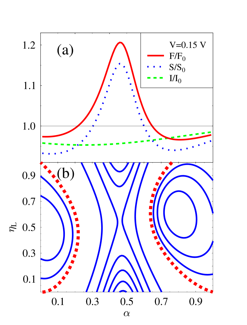
Figure 5a shows change in the noise properties with changing asymmetry in coupling to the leads as expressed by the parameter . Note that the current and noise are slightly asymmetric about the symmetric () point. This asymmetry can be rationalized by noting that the difference implies different tunneling distances between the molecule and the left and right leads, resulting in different tunneling probabilities towards these leads for an electron that lost energy to molecular vibrations. Figure 5b gives a broader view of this issue. It shows a two-dimensional plot of the ratio of Fano factor with and without electron-phonon coupling, , as a function of two asymmetry parameters, and . At and about the symmetric point this ratio is greater than 1, but it becomes smaller (and can be smaller than 1) in strongly asymmetric situations, as shown.
The qualitative observations of Ref. t_stmol_DiVentra, are seen to hold only for symmetric molecule-lead coupling but not for highly asymmetric situations as encountered in STM configurations.
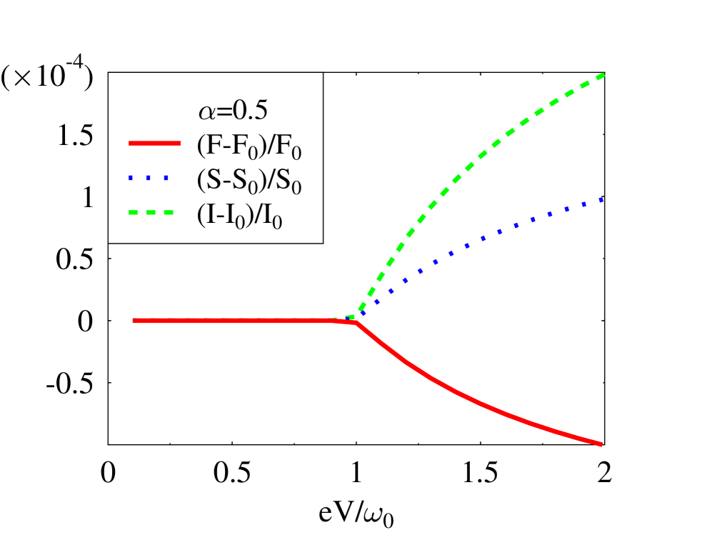
Consider next the off-resonant limit, . In this case is positive. When also and we can use the argument above Eq. (43) to show that . In the absence of electron-phonon interaction and one gets . When this interaction is present and , so that
| (46) |
Figure 6 (which again does not rely on the extreme limit used to develop our intuition) illustrates this situation. Parameters of the calculation are those of Fig. 4a except that eV. With opening of the inelastic channel both current and noise grow, while the Fano factor decreases. Contrary to the situation of resonant tunneling, asymmetry in the coupling to the leads does not provide qualitative difference in this case.
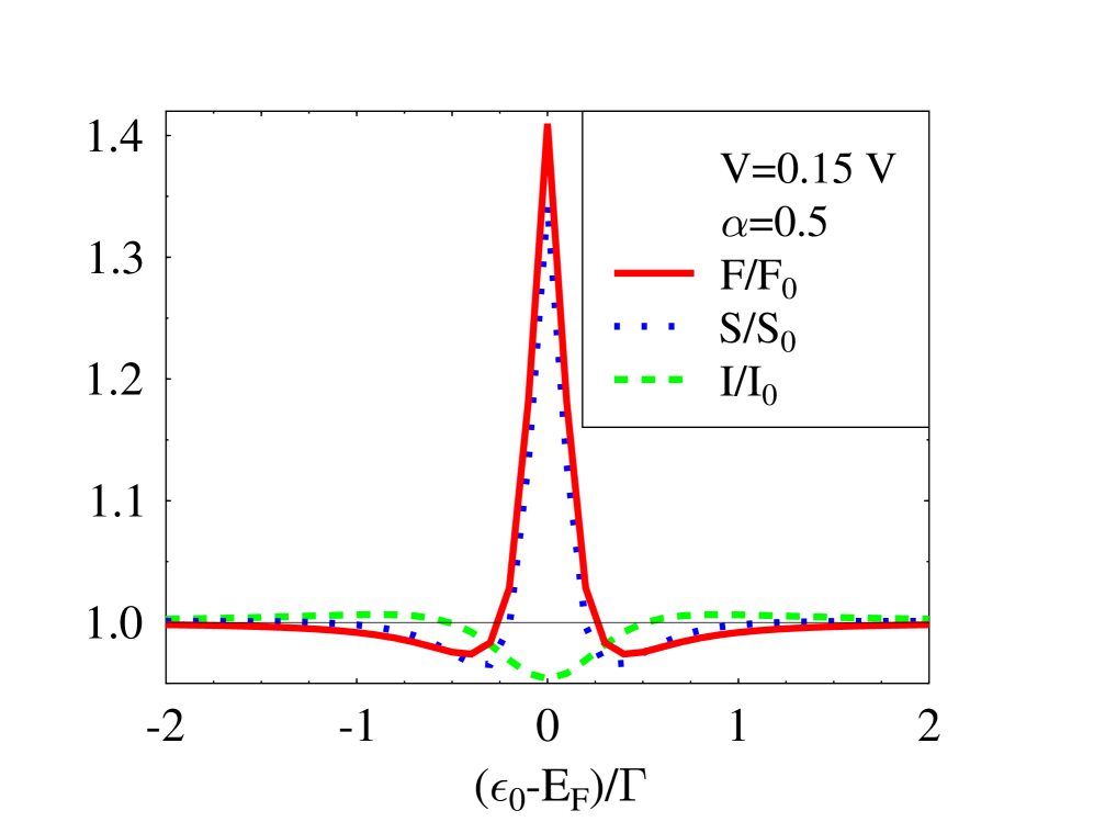
Figure 7 shows the effect on the current and noise properties of transition from the resonant to the off-resonant tunneling regime as may be observed by applying a suitable gate potential. Parameters of the calculation are those of Fig. 4a with position of the molecular orbital changing relative to the Fermi energy. Shown are the ratios of the current (dashed line), noise (dotted line) and Fano factor (solid line) to their values in the absence of electron-phonon interaction. As noticed above and as implied by Eq. (38) the current goes through a minimum at resonance. In contrast the noise (and consequently the Fano factor) maximize at that point. Note that the results are obtained using eV . For phonon effects are negligible and the resulting lines will approach unity.
VI Strong electron-phonon coupling
In this section we sketch the procedure and present results of our numerical calculations for the case of intermediate to strong electron-phonon coupling. Details of the calculation procedure can be found in Ref. strong_el_ph, and here we mention only several important points. A small polaron (canonical or Lang-Firsov) transformationMahan ; Holstein ; LangFirsov applied to Hamiltonian (III) leads to
| (47) | |||||
where
| (48) |
is the electron level shift due to coupling to the primary phonon and
| (49) |
is the primary phonon shift generator with being the primary phonon momentum. We are looking for the single electron Green function, approximately given (on the Keldysh contour) by
| (50) | ||||
In Eq. (VI) is the time ordering operator on the Keldysh contour, is the transformed Hamiltonian, Eq. (47), and implies that the indicated time evolutions are to be carried out with this Hamiltonian. Also
| (51) | ||||
is an approximate (second order cumulant expansion) expression for the shift generator correlation function in terms of the primary phonon Green function
| (52) |
The (approximate) electron Green function is obtained from a self-consistent solution of the approximate (second order in the coupling to the contacts) equations for the phonon and electron Green functions
| (53) | ||||
| (54) | ||||
These equations (for derivation see strong_el_ph ) are analogs of the usual Dyson equation. The functions and , which are analogs of usual phonon and electron self-energies, satisfy the equations
| (55) | ||||
| (56) |
Here and is the free electron Green function for state in the contacts.
The Langreth projectionsLangreth of Eqs. (53)-(56) on the real time axis are solved numerically by using grids in time and energy spaces, repeatedly switching between these spaces as described in Ref. strong_el_ph, . After convergence, the Green function and self-energies needed in the noise expression (10) are available as numerical functions of .
In the presence of electron-phonon interactions the expression for the average steady state current can still be written in a form similar to (19)current with a renormalized transmission coefficient replacing . can be written as , where is now the interacting electronic density of states.likeLandauer Again, the expression for the noise can no longer be cast in the simple additive structure of Eq.(20).additive
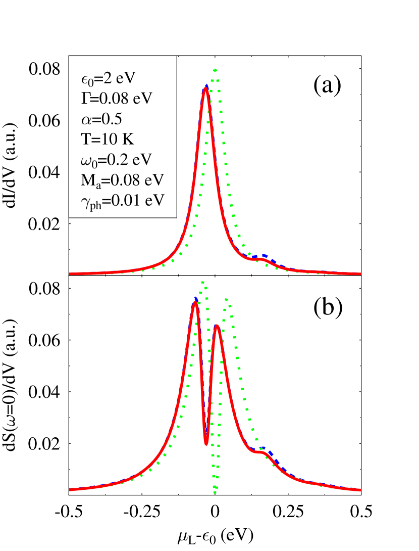
In what follows we present and discuss some numerical results based on this procedure. These results will serve to illustrate the sensitivity of the current and noise calculations to the level of approximation used, the manifestation of the phonon sideband structure in the noise spectrum and the conditions for observing a single or split central peak in the noise spectrum in strong electron-phonon coupling situations. We focus on these issues while limiting the size of our parameter space by taking symmetric junctions with (i.e. ) and , eV above the unbiased Fermi energies, K, eV, eV and eV.
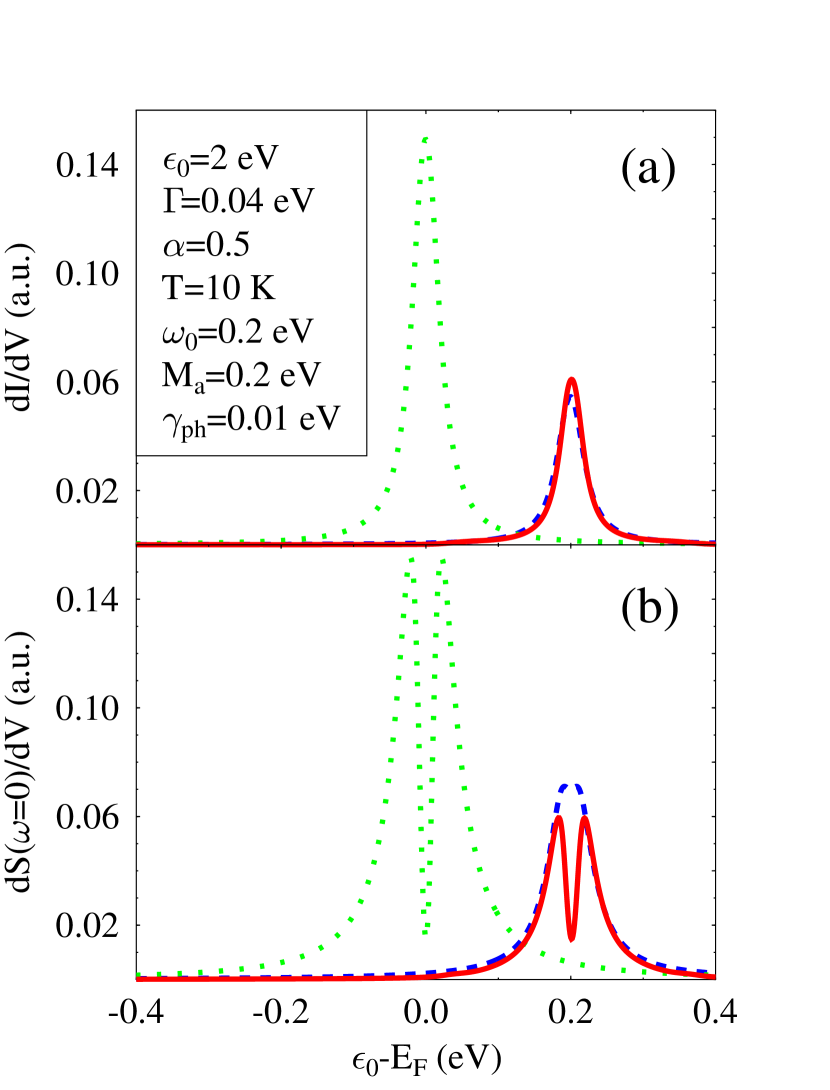
Figure 8 shows the differential conductance and noise spectrum evaluated at V and plotted against the resonance energy (that is in principle controllable by an imposed gate potential). The dotted lines in Fig. 8 represent the current and noise obtained in the purely elastic case (no electron-phonon interaction). The solid lines are results of the converged self-consistent procedure described above while the dashed lines result from the lowest order approximation to Eq. (VI) in which the two factors (electronic and phononic) that enter the Green function are calculated in the absence of electron-phonon interaction.approx Two important features should be noticed. First, because of its split peak structure, the noise spectrum is far more sensitive to the electron-phonon coupling than the conduction plot. Second, for the small source-drain potential used here no phonon sidebands appear. A similar observation was made before for the conduction spectrum.strong_el_ph ; elph_mitra This observation stands in contrast to the results of Zhu and Balatsky,noise_elph_Balatsky who obtained phonon sideband structure in the noise spectrum plotted against the gate potential. Indeed the procedure of Ref. noise_elph_Balatsky, would lead to sideband structure also in the vs. gate potential spectrum and results from the semiclassical approximation discussed above.additive It should be noted that this approximation is valid only when , whereupon the sideband structure will be suppressed by thermal broadening associated with the width of the Fermi function.
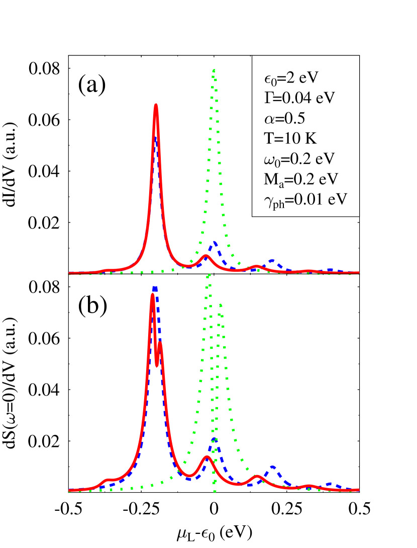
In contrast to gate-voltage plots made at small bias potentials, the phonon sideband structure is observed when the differential conductance is plotted against the source-drain voltage .strong_el_ph ; elph_mitra A similar behavior is observed for the noise spectrum. Figure 9 presents results of the corresponding calculation for the case of relatively weak electron-phonon coupling. Parameters of the calculation are the same as in Fig. 8 except eV and eV. In this weak coupling case only one sideband appears, indicating a single phonon creation by the tunneling electron. Also in this limit the low order calculation appears to be sufficient — self-consistent corrections are seen to be small.
A stronger coupling case is presented in Figure 10, where the parameters of calculation are the same as in Fig 8. Several phonon sidebands indicating phonon emission are observed on the right of the central (elastic) peak. The satellite feature that appears to the left of the central peak is obtained only in the self-consistent calculation (solid line). As was discussed in strong_el_ph, this feature indicates phonon absorption by the tunneling electron and results from heating of the junction by electron flux. We see again that the shape of the differential noise curve, Fig. 10b, is more sensitive to interaction renormalization (self-consistency of calculation) than that of the conductance, Fig 10a, especially in its central peak structure.
A significant difference between the split peak structure of the elastic central peak in Figures 9 and 10 (solid lines) and the elastic result (Fig. 1 and dotted lines of Figs. 9 and 10) when considered in the symmetric molecule-leads coupling case, , is the fact that the differential noise spectrum vanishes between the two peaks in the absence of electron-phonon coupling but remains finite when this coupling is present. To examine the significance of this difference we focus on the limit and the zero order approximation. The lesser and greater Green functions are given by
| (57) | ||||
| (58) | ||||
The retarded Green function can be estimated from the Lehmann representationMahan
| (59) |
For the case of relatively weak coupling to the leads (which is the case where phonon sidebands may be observed), the part of responsible for the central peak region can be approximated by using in (59) only the terms of (57) and (58). This leads to . Using this expression for together with and approximated again by their terms in Eq. (10) leads to
| (60) | ||||
where we have also used Eqs. (13)-(15) and where is given by Eq. (23).
Eq. (60) is the analog of Eq. (25) (the thermal noise contribution vanishes in this limit), and indeed leads to (25) for . For finite electron-phonon coupling the result is seen to depend on the capacitance ratios and . The requirement that has three extrema for a double-peak structure to be seen in the vs. plot can now be applied for the function . This leads to an analog of Eq. (26)
| (61) | ||||
| (62) |
which reduces to (26) when . The peak positions are given by . One can show also that
| (63) | ||||
| (64) |
In the absence of electron-phonon coupling and the expressions above take the forms shown in section IV for elastic tunneling case, where for . This vanishing does not occur even for if . Consequently, the peak positions and noise values spectrum near and between the peaks contains information about the asymmetry of the coupling to the leads, capacitance parameters and strength of electron-phonon interaction.
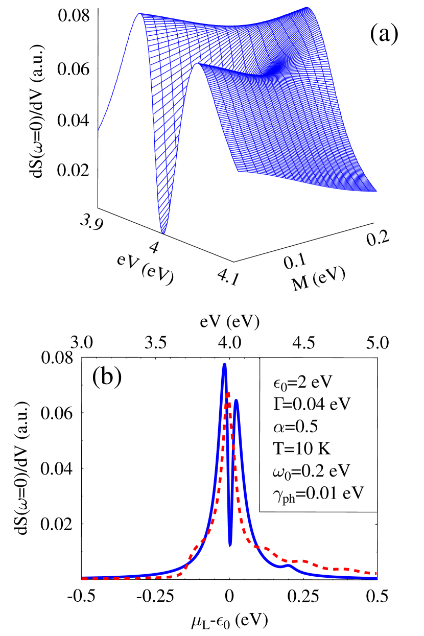
For very strong electron-phonon interaction, , condition (61) can not be satisfied for any choice of the junction parameters. In this case only one peak in in the central region will be observed. Figure 11 illustrates this effect. The parameters used in calculation are the same as in Fig. 10. The calculation is done for symmetric coupling, and . This behavior is seen already in the zero order approximation as is shown in Fig. 11. Fig. 11a shows evolution of the two peak structure into the one central peak with increase of electron-phonon coupling, calculated in this level of approximation. Fig. 11b shows result of self-consistent calculation. A two peak structure is observed for weak ( eV, solid line) and a single peak for strong ( eV, dashed line) electron-phonon coupling.
This spectral change from two to one peak structure with increasing electron-phonon coupling results from transient localization and increasing dephasing of the electron on the bridge and can be used for estimating the junction parameters. For example, in an STM experiment, increasing tip-substrate distance will lead (for not too strong electron-phonon coupling) to a change of the differential noise/voltage profile from a two to a one-peak structure as was seen in Fig. 1 (the general shape of Fig. 1 will persist also for a non-zero ). Eq. (61) written as an equality is a relationship between , , and at this transition point. Information on is easily obtained from the inelastic tunneling structure of either the average current or the noise. To get information on one can use Eqs. (3), (57) and (58) to get for
| (65) | ||||
where
| (66) |
It is easy to see from (VI) and (66) that
| (67) |
In addition Eq. (18) provides a relationship between the parameters , and . An independent determination of the voltage division factor will therefore determine also the other parameters (within our simple junction model). We note that information on the voltage distribution in a junction can be obtained directlyMcEuen or indirectly from plots at positive and negative bias.
VII Conclusion
We have studied inelastic effects on the conduction and noise properties of molecular junctions within a simple model that comprises a one level bridge (arbitrarily chosen above as the molecular LUMO) between two metal contacts. The level is coupled to a vibrational degree of freedom that represents a molecular vibration, which in turn is coupled to a thermal phonon bath that represents the environment.
The case of weak electron-phonon coupling is investigated using standard diagrammatic technique on the Keldysh contour as described in IETS_SCBA, . We find that the predictions of Ref. t_stmol_DiVentra, , increase in zero frequency noise and Fano factor with opening of the inelastic channel, hold only in a particular range of parameters — resonant tunneling with symmetric coupling to the leads. Different modes of behavior are found upon changes that can be affected by moving an STM tip or changing the gate potential. The crossover point between the different modes of behavior provides information on the strength and asymmetry of the molecule-leads coupling and the position of the molecular level relative to the Fermi energy.
For the moderate to strong electron-phonon coupling case we have implemented a recently developed self-consistent scheme on the Keldysh contour.strong_el_ph We have studied the zero-frequency differential noise spectrum for resonant inelastic tunneling and have investigated the shape of this spectrum and its dependence on the parameters of the junction (asymmetry in coupling to the leads and electron-phonon interaction strength). We find that
-
•
As in the spectrum, the differential noise spectrum in resonance inelastic tunneling shows a typical structure characterized by a central feature and phonon sidebands.
-
•
Contrary to Ref. noise_elph_Balatsky we find that displaying the differential noise against the gate potential does not allow observation of phonon sidebands. Rather the sideband structure can be observed in the usual source-drain measurements.
-
•
The central feature exhibits a crossover from double to one central peak structure, both for increasing asymmetry in molecule-lead coupling and for increasing vibronic coupling strength. This change of spectral shape may be used to gain information on the parameters that determine these properties. In particular, asymmetry can be controlled by the tip-molecule distance in STM experiments.
It should be emphasized that as in other studies of current noise in nanojunctions we have focused on the electronic current in static junction structures, here augmented by electron-phonon interactions. Other sources of noise, e.g. structural fluctuations that affect tunneling matrix elements and molecule-lead coupling may exist, and future studies should assess their potential contributions.
Acknowledgements.
MR thanks Mark Reed for a fruitful discussion. We thank Yu. Galperin for clarifying for us the origin of Eq. (5). We thank the DARPA MoleApps program and the NASA URETI program for support. AN thanks the Israel Science Foundation and the U.S.-Israel Binational Science Foundation for support.References
-
(1)
Molecular Electronics II, Eds. A. Aviram, M. Ratner,
V. Mujica, Ann. N.Y. Acad. Sci., vol. 960 (2002);
Molecular Electronics III, Eds. J. R. Reimers, C. A. Picconatto, J. C. Ellenbogen, R. Shashidhar, Ann. N.Y. Acad. Sci., vol. 1006 (2003). - (2) A. Nitzan, Ann. Rev. Phys. Chem. 53, 681 (2001).
-
(3)
Molecular Nanoelectronics, Eds. M. A. Reed and T. Lee,
American Scientific Publishers (2003);
W. Y. Wang and M. A. Reed, Rep. Progr. Phys. 68, 523 (2005). - (4) Introducing Molecular Electronics, Eds. G. Cuniberti, G. Fagas, and K. Richter, Springer, Berlin and Heidelberg (2005).
- (5) D. R. Bowler, J. Phys.: Condens. Matter 16, R721 (2004).
- (6) A. Yazdani, D. M. Eigler, and N. D. Lang, Science 272, 1921 (1996).
- (7) R. P. Andres, T. Bein, M. Dorogi, S. Feng, J. I. Henderson, C. P. Kubiak, W. Mahoney, R. G. Osifchin, R. Reifenberger, Science 272, 1323 (1996); S. Datta, W. Tian, S. Hong, R. Reifenberger, J. I. Henderson, and C. P. Kubiak, Phys. Rev. Lett. 79, 2530 (1997); W. Tian, S. Datta, S. Hong, R. Reifenberger, J. I. Henderson, and C. P. Kubiak, J. Chem. Phys. 109, 2874 (1998).
-
(8)
M. A. Reed, C. Zhou, C. J. Muller, T. P. Burgin,
and J. M. Tour, Science 278, 252 (1997);
C. Zhou, M. R. Deshpande, M. A. Reed, L. Jones II, and J. M. Tour,
Appl. Phys. Lett. 71, 611 (1997);
ibid. 71, 2857 (1997);
J. Chen, M. A. Reed, A. M. Rawlett, J. M. Tour, Science 286, 1550 (1999). - (9) C. P. Collier, E. W. Wong, M. Belohradsky, F. M. Raymo, J. F. Stoddart, P. J. Kuekes, R. S. Williams, and J. R. Heath, Science 285, 391 (1999).
- (10) C. Kergueris, J.-P. Bourgoin, S. Palacin, D. Esteve, C. Urbina, M. Magoga, and C. Joachim, Phys. Rev. B 59, 12505 (1999).
- (11) J. Reichert, R. Ochs, D. Beckman, H. B. Weber, M. Mayor, and H. v. Löhneysen, Phys. Rev. Lett. 88, 176804 (2002).
- (12) W. Liang, M. P. Shores, M. Bockrath, J. R. Long, and H. Park, Nature 417, 725 (2002).
- (13) S. Kubatkin, A. Danilov, M. Hjort, J. Cornil, J.-L. Bredas, N. Stuhr-Hansen, P. Hedegard, and T. Bjørnholm, Nature 425, 698 (2003).
-
(14)
H. Park, J. Park, A. K. L. Lim, E. H. Anderson,
A. P. Alivisatos, and P. L. McEuen, Nature 407, 57 (2000);
J. Park, A. N. Pasupathy, J. I. Goldsmith, C. Chang, Y. Yaish, J. R. Petta, M. Rinkoski, J. P. Sethna, H. D. Abruña, P. L. McEuen, and D. C. Ralph, Nature 417, 722 (2002);
J. Park, A. N. Pasupathy, J. I. Goldsmith, A. V. Soldatov, C. Chang, Y. Yaish, J. P. Sethna, H. D. Abruña, D. C. Ralph, and P. L. McEuen, Thin Solid Films 438-439, 457 (2003);
A. N. Pasupathy, R. C. Bialczak, J. Martinek, J. E. Grose, L. A. K. Donev, P. L. McEuen, and D. C. Ralph, Science 306, 86 (2004). -
(15)
L. H. Yu, Z. K. Keane, J. W. Ciszek, L. Cheng, M. P. Stewart,
J. M. Tour, and D. Natelson, Phys. Rev. Lett. 93, 266802 (2004);
L. H. Yu and D. Natelson, Nano Lett. 4, 79 (2004);
L. H. Yu, Z. K. Keane, J. W. Ciszek, L. Cheng, J. M. Tour, T. Baruah, M. R. Pederson, and D. Natelson, cond-mat/0505683 (2005). -
(16)
H. J. Lee and W. Ho, Science 286, 1719 (1999);
Phys. Rev. B 61, R16347 (2000);
J. Gaudioso, L. J. Lauhon, and W. Ho, Phys. Rev. Lett. 85, 1918 (2000);
J. R. Hahn, H. J. Lee, and W. Ho, Phys. Rev. Lett. 85, 1914 (2000);
L. J. Lauhon and W. Ho, Phys. Rev. Lett. 85, 4566 (2000); Phys. Rev. B 60, R8525 (1999);
N. Lorente, M. Persson, L. J. Lauhon, and W. Ho, Phys. Rev. Lett. 86, 2593 (2001);
J. R. Hahn and W. Ho, Phys. Rev. Lett. 87, 196102 (2001). - (17) N. B.Zhitenev, H. Meng, and Z. Bao, Phys. Rev. Lett. 88, 226801 (2002).
-
(18)
R. H. M. Smit, Y. Noat, C. Untiedt, N. D. Lang,
M. C. van Hemert, and J. M. van Ruitenbeek,
Nature 419, 906 (2002);
D. Djukic, K. S. Thygesen, C. Untiedt, R. H. M. Smit, K. W. Jacobsen, and J. M. van Ruitenbeek, Phys. Rev. B 71, 161402(R) (2005). - (19) Ya. M. Blanter and M. Buttiker, Physics Reports 336, 1 (2000).
- (20) Y. P. Li, A. Zaslavsky, D. C. Tsui, M. Santos, and M. Shayegan, Phys. Rev. B 41, 8388 (1990).
- (21) S. S. Safonov, A. K. Savchenko, D. A. Bagrets, O. N. Jouravlev, Y. V. Nazarov, E. H. Linfield, and D. A. Ritchie, Phys. Rev. Lett. 91, 136801 (2003).
- (22) A. Nauen, F. Hohls, N. Maire, K. Pierz, and R. J. Haug, Phys. Rev. B 70, 033305 (2004).
- (23) S. W. Jung, T. Fujisawa, Y. Hirayama, and Y. H. Jeong, Appl. Phys. Lett. 85, 768 (2004).
- (24) Y. P. Li, D. C. Tsui, J. J. Heremans, J. A. Simmons, and G. W. Weimann, Appl. Phys. Lett. 57, 774 (1990).
- (25) S. Washburn, R. J. Haug, K. Y. Lee, and J. M. Hong, Phys. Rev. B 44, 3875 (1991).
- (26) F. Liefrink, J. I. Dijkhuis, and H. van Houten, Semicond. Sci. Technol. 9, 2178 (1994).
- (27) M. Reznikov, M. Heiblum, H. Strikman, and D. Mahalu, Phys. Rev. Lett. 75, 3340 (1995).
- (28) J. Delahaye, R. Lindell, M. S. Silanpaa, M. A. Paalanen, E. B. Sonin, and P. J. Hakonen, cond-mat/0209076 (2002).
- (29) R. K. Lindell, J. Delahaye, M. A. Sillanpaa, T. T. Heikkila, E. B. Sonin, and P. J. Hakonen, Phys. Rev. Lett. 93, 197002 (2004).
- (30) B. Reulet, J. Senzier, and D. E. Prober, Phys. Rev. Lett. 91, 196601 (2003).
- (31) L. Y. Chen and C. S. Ting, Phys. Rev. B 43, 4534 (1991).
- (32) A. Levy Yeyati, F. Flores, and E. V. Anda, Phys. Rev. B 47, 10543 (1993).
- (33) K.-M. Hung and G. Y. Wu, Phys. Rev. B 48, 14687 (1993).
- (34) A. Thielmann, M. H. Hettler, J. König, and G. Schön, Phys. Rev. B 68, 115105 (2003).
- (35) D. Averin and H. T. Imam, Phys. Rev. Lett. 76, 3814 (1996).
- (36) F. Green, J. S. Thakur, and M. P. Das, Phys. Rev. Lett. 92, 156804 (2004).
- (37) E. B. Sonin, Phys. Rev. B 70, 140506 (2004); cond-mat/0505424 (2005).
- (38) J. Aghassi, A. Thielmann, M. H. Hettler, and G. Schön, cond-mat/0505345 (2005).
- (39) M. Kindermann and P. W. Brouwer, cond-mat/0506455 (2005).
- (40) D. B. Gutman and Y. Gefen, Phys. Rev. B 64, 205317 (2001).
- (41) S. Dallakyan and S. Mazumdar, Appl. Phys. Lett. 82, 2488 (2003).
- (42) K. Walczak, Phys. Stat. Sol (b) 241, 2555 (2004).
- (43) Y.-C. Chen and M. Di Ventra, Phys. Rev. B 67, 153304 (2003); J. Lagerqvist, Y.-C. Chen, and M. Di Ventra, Nanotechnology 15, S459 (2004).
- (44) N. Nishiguchi, Phys. Rev. Lett. 89, 066802 (2002).
- (45) A. Yu. Smirnov, L. G. Mourokh, and N. J. M. Horing, Phys. Rev. B 67, 115312 (2003).
- (46) A. A. Clerk and S. M. Girvin, Phys. Rev. B 70, 121303 (2004).
- (47) T. Novotný, A. Donarini, C. Flindt, and A.-P. Jauho, Phys. Rev. Lett. 92, 248302 (2004).
- (48) C. Flindt, T. Novotny, and A.-P. Jauho, Phys. Rev. B 70, 205334 (2004).
- (49) J. Wabnig, D. V. Khomitsky, J. Rammer, and A. L. Shelankov, cond-mat/0506802 (2005).
- (50) S. Camalet, S. Kohler, and P. Hänggi, Phys. Rev. B 70, 155326 (2004).
- (51) R. Guyon, T. Jonckheere, V. Mujica, A. Crépieux, and T. Martin, J. Chem. Phys. 122, 144703 (2005).
- (52) A. Shimizu and M. Ueda, Phys. Rev. Lett. 69, 1403 (1992).
- (53) O. Lund Bo and Yu. Galperin, Phys. Rev. B 55, 1696 (1997).
- (54) B. Dong, H. L. Cui, X. L. Lei, and N. J. M. Horing, Phys. Rev. B 71, 045331 (2005).
- (55) Y.-C. Chen and M. Di Ventra, Phys. Rev. Lett. 95, 166802 (2005).
- (56) J.-X. Zhu and A. V. Balatsky, Phys. Rev. B 67, 165326 (2003).
- (57) M. Galperin, M. A. Ratner, and A. Nitzan, J. Chem. Phys. 121, 11965 (2004).
- (58) M. Galperin, A. Nitzan, and M. A. Ratner, Phys. Rev. B 73, 082604 (2006).
- (59) For the resonance tunneling problem under discussion the weak and strong electron-phonon coupling limit may be characterized by comparing the electron-phonon coupling to the magnitude of the complex resonance energy .
- (60) U. Lundin and R. H. McKenzie, Phys. Rev. B 66, 075303 (2002).
- (61) N. E. Bickers, Rev. Mod. Phys. 59, 845 (1987).
-
(62)
Y. Meir and N. S. Wingreen,
Phys. Rev. Lett. 68, 2512 (1992);
A. Jauho, N. S. Wingreen, and Y. Meir, Phys. Rev. B 50, 5528 (1994). - (63) H. Haug and A.-P. Jauho, Quantum Kinetics in Transport and Optics of Semiconductors. (Springer, Berlin, 1996).
- (64) U. Hanke, Yu. Galperin, K. A. Chao, M. Gisselfält, M. Jonson, and R. I. Shekhter, Phys. Rev. B 51, 9084 (1995).
- (65) O. Lund Bo and Yu. Galperin, J. Phys.: Condens. Matter 8, 3033 (1996).
- (66) Note that Bo and Galperinnoise_Galperin used a different Green functions notaions.
- (67) N. A. Pradhan, N. Liu, and W. Ho, J. Phys. Chem. B 109, 8513 (2005).
- (68) J. Repp, G. Meyer, S. M. Stojkovic, A. Gourdon, and C. Joachim, Phys. Rev. Lett. 94, 026803 (2005).
- (69) A. E. Hanna and M. Tinkham, Phys. Rev. B 44, 5919 (1991).
- (70) G.-L. Ingold and Yu. V. Nazarov in Single Charge Tunneling, edited by H. Grabert and M. H. Devoret (Plenum Press, New York and London, 1992) pp. 21-108.
- (71) R. Chance, A. Prock, and R. Silbey, Adv. Chem. Phys. 31, 1 (1978).
- (72) A. Bachtold, M. S. Fuhrer, S. Plyasunov, M. Forero, E. H. Anderson, A. Zettl, and P. L. McEuen, Phys. Rev. Lett. 84, 6082 (2000).
- (73) G. D. Mahan, Many-Particle Physics. (Third edition, Kluwer Academic/Plenum Publishers, New York, 2000).
- (74) T. Holstein, Ann. Phys. 8, 343 (1959).
- (75) I. G. Lang and Yu. A. Firsov, Sov. Phys. JETP 16, 1301 (1963).
- (76) D. C. Langreth, Linear and Nonlinear Response Theory with Applications, p. 3–32 in: Linear and Nonlinear Electron Transport in Solids, Eds. J. T. Devreese and D. E. Doren (Plenum Press, New York and London, 1976).
- (77) The alternative scenario in which crosses the HOMO for increasingly positive bias would lead to a similar picture for the same electron-phonon coupling.
- (78) Note that asymmetry in these heights may reflect deviations from the wide band approximation.
- (79) and are related to the electron and phonon Green functions by and .
- (80) This statement holds in the wide band limit or at least when does not depend on .current ; HaugJauho Note that in a more general formulation (e.g. for a bridge with more than one level) should be substituted by , where is a spectral function.
- (81) Previous statements about the additive structure of the noise spectrum in the presence of electron-phonon interactionnoise_elph_Balatsky are based on a treatment that makes the classical-like assumption about the nuclear motion, i.e. disregarding the difference between and which is valid only when . The ansatz proposed by Ngac_current_Ng for this approximation is again valid only in this limit.
- (82) This approximation was used in the past in several papers, see e.g. Z.-Z. Chen, R. Lü, and B.-F. Zhu, Phys. Rev. B 71, 165324 (2005).
- (83) T. K. Ng, Phys. Rev. Lett. 76, 487 (1996).
- (84) A. Mitra, I. Aleiner, and A. J. Millis, Phys. Rev. B 69, 245302 (2004).