A system for measuring auto- and cross-correlation of current noise at low temperatures
Abstract
We describe the construction and operation of a two-channel noise detection system for measuring power and cross spectral densities of current fluctuations near 2 MHz in electronic devices at low temperatures. The system employs cryogenic amplification and fast-Fourier-transform based spectral measurement. The gain and electron temperature are calibrated using Johnson noise thermometry. Full shot noise of can be resolved with an integration time of . We report a demonstration measurement of bias-dependent current noise in a gate defined GaAs/AlGaAs quantum point contact.
Over the last decade, measurement of electronic noise in mesoscopic conductors has successfully probed quantum statistics, chaotic scattering and many-body effects Blanter00 (00); Martin05 (00). Suppression of shot noise below the Poissonian limit has been observed in a wide range of devices, including quantum point contacts Reznikov95 (95); Kumar96 (96); Liu98 (98), diffusive wires Steinbach96 (96); Henny99a (99), and quantum dots Oberholzer01 (01), with good agreement between experiment and theory. Shot noise has been used to measure quasiparticle charge in strongly correlated systems, including the fractional quantum hall regimede-Picciotto97 (97); Saminadayar97 (97) and normal-superconductor interfacesJehl00 (00), and to investigate regimes where Coulomb interactions are strong, including coupled localized states in mesoscopic tunnel junctions Safonov03 (03) and quantum dots in the sequential tunneling Gustavsson05 (05) and cotunneling Onac06 (06) regimes. Two-particle interference not evident in dc transport has been investigated using noise in an electronic beam splitter Liu98 (98).
Recent theoretical workMartin02 (02); Samuelsson04 (04); Beenakker04 (04); Lebedev05 (05) proposes the detection of electron entanglement via violations of Bell-type inequalities using cross-correlations of current noise between different leads. Most noise measurements have investigated either noise auto-correlationReznikov95 (95); Steinbach96 (96); de-Picciotto97 (97); Schoelkopf97 (97); Liu98 (98); Spietz03 (03); Onac06 (06) or cross-correlation of noise in a common currentKumar96 (96); Glattli1 (97); Henny99a (99); Sampietro99 (99); Oberholzer01 (01); Safonov03 (03), with only a few experimentsHenny99 (99); Oberholzer06 (06); Oliver99 (99) investigating cross-correlation between two distinct currents. Henny et al.Henny99 (99) and Oberholzer et al.Oberholzer06 (06) measured noise cross-correlation in the acoustic frequency range (low kHz) using room temperature amplification and a commercial fast Fourier transform (FFT)-based spectrum analyzer. Oliver et al.Oliver99 (99) measured cross-correlation in the low MHz using cryogenic amplifiers and analog power detection with hybrid mixers and envelope detectors.
In this paper, we describe a two-channel noise detection system for simultaneously measuring power spectral densities and cross spectral density of current fluctuations in electronic devices at low temperatures. Our approach combines elements of the two methods described above: cryogenic amplification at low MHz frequencies and FFT-based spectral measurement.
Several factors make low-MHz frequencies a practical range for low-temperature current noise measurement. This frequency range is high compared to the noise corner in typical mesoscopic devices. Yet, it is low enough that FFT-based spectral measurement can be performed efficiently with a personal computer (PC) equipped with a commercial digitizer. Key features of this FFT-based spectral measurement are near real-time operation and sufficient frequency resolution to detect spectral features of interest. Specifically, the fine frequency resolution provides information about the measurement circuit and amplifier noise at MHz, and enables extraneous interference pick-up to be identified and eliminated. These two features constitute a significant advantage over both wide-band analog detection of total noise power, which sacrifices resolution for speed, and swept-sine measurement, which sacrifices speed for resolution.
The paper is divided as follows. A block diagram of the system is presented in Section I. The amplification circuit is discussed in Section II. Section III describes the data analysis procedure, including digitization and FFT processing. A demonstration measurement of current noise in a quantum point contact (QPC) is presented in Section IV. System performance is discussed in Section V.
I Overview of the system
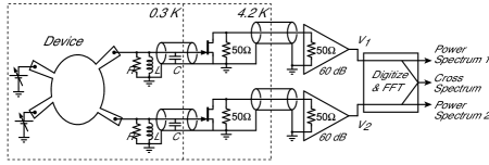
Figure 1 shows a block diagram of the two-channel noise detection system, which is integrated with a commercial cryostat (Oxford Intruments Heliox ). The system takes two input currents and amplifies their fluctuations in several stages. First, a parallel resistor-inductor-capacitor (RLC) circuit performs current-to-voltage conversion at frequencies close to its resonance at . Through its transconductance, a high electron mobility transistor (HEMT) operating at 4.2 K converts these voltage fluctuations into current fluctuations in a coaxial line extending from 4.2 K to room temperature. A amplifier with of gain completes the amplification chain. The resulting signals and are simultaneously sampled at by a two-channel digitizer (National Instruments PCI-5122) in a 3.4 GHz PC (Dell Optiplex GX280). The computer takes the FFT of each signal and computes the power spectral density of each channel and the cross spectral density.
II Amplifier
II.1 Design objectives
A number of objectives have guided the design of the amplification lines. These include:
-
1.
Low amplifier input-referred voltage noise and current noise.
-
2.
Simultaneous measurement of both noise at MHz and transport near dc.
-
3.
Low thermal load.
-
4.
Small size, allowing two amplification lines within the 52 mm bore cryostat.
-
5.
Maximum use of commercial components.
-
6.
Compatibility with high magnetic fields.
II.2 Overview of Circuit
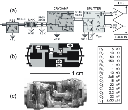
Each amplification line consists of four circuit boards interconnected by coaxial cable, as shown in the circuit schematic in Fig. 2(a). Three of the boards are located inside the cryostat. The resonant circuit board (labeled RES in Fig. 2(a)) is mounted on the sample holder at the end of the 30 cm long coldfinger that extends from the pot to the center of the superconducting solenoid. The heat-sink board (SINK) anchored to the pot is a meandering line that thermalizes the inner conductor of the coaxial cable. The CRYOAMP board at the plate contains the only active element operating cryogenically, an Agilent ATF-34143 HEMT. The four-way SPLITTER board operating at room temperature separates low and high frequency signals and biases the HEMT. Each line amplifies in two frequency ranges, a low-frequency range below and a high-frequency range around 2 MHz.
The low-frequency equivalent circuit is shown in Fig. 3(a): A resistor () to ground, shunted by a capacitor (), converts an input current to a voltage on the HEMT gate. The HEMT amplifies this gate voltage by on its drain, which connects to a room temperature voltage amplifier at the low frequency port of the SPLITTER board. The low-frequency voltage amplifier (Stanford Research Systems model SR560) is operated in single-ended mode with ac coupling, gain and bandpass filtering ( to ). The bandwidth in this low-frequency regime is set by the input time constant.
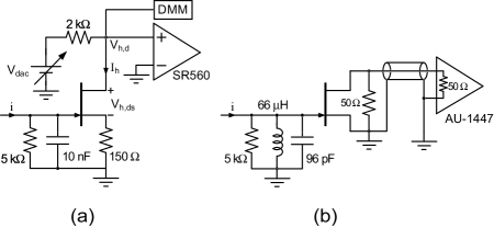
The high-frequency equivalent circuit is shown in Fig. 3(b). The inductor H dominates over and forms a parallel RLC tank with and the capacitance 96 pF of the coaxial line connecting to the CRYOAMP board. Resistor is shunted by to enhance the transconductance at the CRYOAMP board. The coaxial line extending from to room temperature is terminated on both sides by . At room temperature, the signal passes through the high-frequency port of the SPLITTER board to a amplifier (MITEQ AU-1447) with a gain of and a noise temperature of in the range .
II.3 Operating point
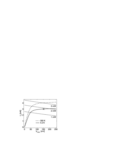
The HEMT must be biased in saturation to provide voltage (transconductance) gain in the low (high) frequency range. , and supply voltage determine the HEMT operating point ( grounds the HEMT gate at dc). A notable difference in this design compared to similar published ones regards the placement of . In previous implementations of similar circuits Lee89 (89); Lee93 (93); Robinson04 (04), is a variable resistor placed outside the refrigerator and connected to the source lead of via a second coaxial line or low-frequency wire. Here, is located on the CRYOAMP board to simplify assembly and save space, at the expense of having full control of the bias point in ( fixes the saturation value of the HEMT current ). Using the I-V curves in Ref. 28 for a cryogenically cooled ATF-34143, we choose to give a saturation current of a few mA. This value of saturation current reflects a compromise between noise performance and power dissipation. As shown in Fig. 4, is biased by varying the supply voltage fed at the SPLITTER board. At the bias point indicated by a cross, the total power dissipation in the HEMT board is , and the input-referred voltage noise of the HEMT is .
II.4 Passive Components
Passive components were selected based on temperature stability, size and magnetic field compatibility. All resistors (Vishay TNPW thin film) are 0805-size surface mount. Their variation in resistance between room temperature and is . Inductor (two Coilcraft 1812CS ceramic chip inductors in series) does not have a magnetic core and is suited for operation at high magnetic fields. The dc resistance of is at 300(4.2) K. With the exception of , all capacitors are 0805-size surface mount (Murata COG GRM21). (two American Technical Ceramics 700B NPO capacitors in parallel) is certified non-magnetic.
II.5 Thermalization
To achieve a low device electron temperature, circuit board substrates must handle the heat load from the coaxial line. The CRYOAMP board must also handle the power dissipated by the HEMT and . Sapphire, having good thermal conductivity at low temperatures Pobell92 (92) and excellent electrical insulation, is used for the substrate in the RES, SINK and CRYOAMP boards. Polished blanks, 0.02” thick and 0.25” wide, were cut to lengths of 0.6” (RES and CRYOAMP) or 0.8” (SINK) using a diamond saw. Both planar surfaces were metallized with thermally evaporated Cr/Au (30/300 nm). Circuit traces were then defined on one surface using a Pulsar toner transfer mask and wet etching with Au and Cr etchants (Transene types TFA and 1020). Surface mount components were directly soldered.
The RES board is thermally anchored to the sample holder with silver epoxy (Epoxy Technology 410E). The CRYOAMP (SINK) board is thermalized to the plate ( pot) by a copper braid soldered to the back plane.
Semirigid stainless steel coaxial cable (Uniform Tube UT-85 SS-SS) is used between the SINK and CRYOAMP boards, and between the CRYOAMP board and room temperature. Between the RES and SINK boards, smaller coaxial cable (Uniform Tube UT-34 C) is used to conserve space.
With this approach to thermalization, the base temperature of the refrigerator is 290 mK with a hold time of h. As demonstrated in Section IV, the electron base temperature in the device is also 290 mK.
III Digitization and FFT Processing
The amplifier outputs and (see Fig. 1) are sampled simultaneously using a commercial digitizer (National Instruments PCI-5122) with 14-bit resolution at a rate . To avoid aliasingOppenheim89 (89) from the broad-band amplifier background, and are frequency limited to below the Nyquist frequency of using 5-pole Chebyshev low-pass filters, built in-house from axial inductors and capacitors with values specified by the design recipe in Ref. 31. The filters have a measured half power frequency of , suppression at and a pass-band ripple of .
While the digitizer continuously stores acquired data into its memory buffer (16 MB per channel), a software program processes the data from the buffer in blocks of points per channel. is chosen to yield a resolution bandwidth , and to be factorizable into powers of two and three to maximize the efficiency of the FFT algorithm.
Each block of data is processed as follows. First, and are multiplied by a Hanning window to avoid end effectsOppenheim89 (89). Second, using the FFTW package FFTW98 (98), their FFTs are calculated:
where , , and . Third, the power spectral densities and the cross spectral density are computed.
As blocks are processed, running averages of , , and are computed until the desired integration time is reached. With the 3.4 GHz computer and the FFTW algorithm, these computations are carried out in nearly real-time: it takes to acquire and process of data.
IV Measurement: QPC current noise
In this section, the system is demonstrated with measurements of current noise in a quantum point contact (QPC). Specifically, the partition noise is measured as a function of QPC source-drain bias :
| (1) |
Here, is the total QPC current noise spectral density without extraneous noise (, random telegraph, pick-up), is the Boltzmann constant, is the electron temperature, is the bias-dependent QPC differential conductance, and is the current through the QPC.
IV.1 Device and Setup
The QPC is defined by two electrostatic gates on the surface of a heterostructure grown by molecular beam epitaxy. The two-dimensional electron gas (2DEG) below the surface has a density and mobility . The QPC conductance is controlled by negative voltages and applied to the electrostatic gates.
The QPC is connected to the system as shown in the inset of Fig. 5. The two amplification lines are connected to the same reservoir of the QPC. In this case, the two input RLC tanks effectively become a single tank with resistance , inductance and capacitance . The QPC current noise couples to both amplification lines and thus can be extracted from either the single channel power spectral densities or the cross spectral density. The latter has the technical advantage of rejecting any noise not common to both amplification lines. It is used to extract in the remainder of this section.
A , excitation is applied to the other QPC reservoir and used for lock-in measurement of . A dc bias voltage is also applied to generate a finite . deviates from due to the resistance in-line with the QPC, which is equal to the sum of and ohmic contact resistance . could in principle be measured by the traditional four-wire technique. This would require additional low-frequency wiring, as well as filtering to prevent extraneous pick-up and room-temperature amplifier noise from coupling to the noise measurement circuit. For technical simplicity, here is obtained by numerical integration of the measured bias-dependent :
| (2) |
IV.2 Measurement
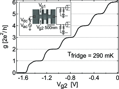
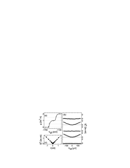
Figure 5 shows linear conductance as a function of , at a fridge temperature (base temperature). Here, was extracted from lock-in measurements using amplification line 1. As neither the low frequency gain of amplifier 1 nor were known precisely beforehand, these parameters were calibrated by aligning the observed conductance plateaus to the expected multiples of . This method yielded a low frequency gain and .
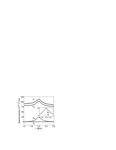
Figure 6 shows , , , and as a function of frequency , at base temperature and with the QPC pinched off (). shows a peak at the resonant frequency of the RLC tank, on top of a background of approximately . The background in is due to the voltage noise of amplification line 1(2) (). The peak results from thermal noise of the resonator resistance and current noise () from the amplifiers. picks out this peak and rejects the amplifier voltage noise backgrounds. The inset zooms in on near the resonant frequency. The solid curve is a best-fit to the form
| (3) |
corresponding to the lineshape of white noise band-pass filtered by the RLC tank. The fit parameters are the peak height , the half-power bandwidth and the peak frequency . Power spectral densities can be fit to a similar form including a fitted background term:
| (4) |
IV.3 Noise measurement calibration
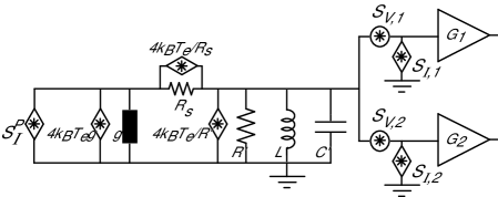
In order to extract from , the noise measurement system must be calibrated in situ. An effective circuit with noise sources is defined for this purpose and shown in Fig. 7. Within this circuit model, is given by:
| (5) |
Here, is the cross-correlation gain and is the total effective resistance parallel to the tank Detail01 (05).
Calibration requires assigning values for , , and . While the value is known from the conductance measurement, and are calibrated from thermal noise measurements. The procedure demonstrated in Fig. 8 stems from the relation Detail02 (05) valid at .
First, is measured over for various settings at each of three elevated fridge temperatures (). and are extracted from fits to using Eq. (3) and plotted parametrically (open markers in Fig. 8(a)). A linear fit (constrained to pass through the origin) to each parametric plot gives the slope at each temperature, equal to . Assuming at these temperatures, is extracted from a linear fit to , shown in Fig. 8(b).
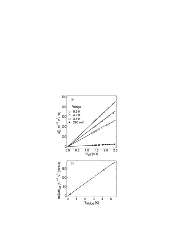
Next, the base electron temperature is calibrated from a parametric plot of as a function of obtained from similar measurements at base temperature (solid circles in Fig. 8(a)). From the fitted slope (black marker in Fig. 8(b)) and using the calibrated , a value is obtained. This suggests that electrons are well thermalized to the fridge.
IV.4 QPC partition noise
Following the calibration, is extracted as follows. and are simultaneously measured () at fixed as a function of between and . At each setting, and are obtained from fits of to Eq. (3), and used with the measured to extract from Eq. (5).
Demonstration measurements of are shown in Fig. 9. Open markers superimposed on the linear conductance trace in Fig. 9(a) indicate settings giving , 0.5, 1, 1.5, and . The corresponding noise data are shown in Fig. 9(b). At 0, 1 and , where the QPC is either pinched off or on a linear conductance plateau, shows little dependence on bias, in contrast with the dependence observed when 0.5 and . This behavior is consistent with earlier experiments Reznikov95 (95); Kumar96 (96) and theory Lesovik89 (89); Buttiker90 (90) of shot noise in a QPC.
Within mesoscopic scattering theory Blanter00 (00); Martin05 (00), where transport is described by transmission coefficients ( is the sub-band index and denotes spin), is given by
| (6) |
with a noise factor . This equation is strictly valid for constant transmission coefficients across the bias window. At low-temperatures and for the spin-degenerate case, is zero at multiples of and reaches a maximum value of 0.25 at odd multiples of . Fits to the data in Fig. 9(b) using the form of Eq. (6) are shown as solid curves, with and best-fit values of 0.00, 0.20, 0.00, 0.19, and 0.03 for 0, 0.5, 1, 1.5, and , respectively. The deviation of the best-fit from 0.25 near 0.5 and 1.5 is discussed in detail in Ref. 37.
A measurement of as a function of with the QPC barely open (solid marker in Fig. 9(a)) is shown in Fig. 9(c). In this regime, full shot noise is observed. This is consistent with scattering theory and with recent measurements on mesoscopic tunnel barriers free of impurities, localized states and 1/f noiseChen06 (06).
V System Performance
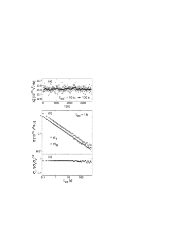
The resolution in the estimation of current noise spectral density from one-channel and two-channel measurements is determined experimentally in this final section. Noise data are first sampled over a total time , with the QPC at base temperature and pinched off. Dividing the data in segments of time length , calculating the power and cross spectral densities for each segment, and fitting with Eqs. (3) and (4) gives a sequence of peak heights for each of , and . Shown in open (solid) circles in Fig. 10(a) is as a function of time for . The standard deviation of is . The resolution in current noise spectral density is given by (see Eq. (5)). For , , which corresponds to full shot noise of .
The effect of integration time on the resolution is determined by repeating the analysis for different values of . Fig. 10(b) shows the standard deviation () of () as a function of . The standard deviation of , not shown, overlaps closely with . All three standard deviations scale as , consistent with the Dicke radiometer formula Dicke46 (46) which applies when measurement error results only from finite integration time, i.e., it is purely statistical. This suggests that, even for the longest segment length of , the measurement error is dominated by statistical error and not by instrumentation drift on the scale of 1 h.
Figure 10(c) shows as a function of . This ratio gives the fraction by which, in the present measurement configuration, the statistical error in current noise spectral density estimation from is lower than the error in the estimation from either or alone. The geometric mean in the denominator accounts for any small mismatch in the gains and . In theory, and in the absence of drift, this ratio is independent of and equal to when the uncorrelated amplifier voltage noise dominates over the noise common to both amplification lines. The ratio would be unity when the correlated noise dominates over .
The experimental is close to (dashed line). This is consistent with the spectral density data in Fig. 6, which shows that the backgrounds in and are approximately three times larger than the cross-correlation peak height. The ratio deviates slightly below at the largest values. This may result from enhanced sensitivity to error in the substraction of the background at the longest integration times.
A similar improvement relative to estimation from either or alone would also result from estimation with a weighted average . The higher resolution attainable from two channel measurement relative to single-channel measurement in this regime has been previously exploited in noise measurements in the kHz range Kumar96 (96); Glattli1 (97); Sampietro99 (99).
VI Conclusion
We have presented a two-channel noise detection system measuring auto- and cross-correlation of current fluctuations near in electronic devices at low temperatures. The system has been implemented in a refrigerator where the base device electron temperature, measured by noise thermometry, is . Similar integration with a - dilution refrigerator would enable noise measurement at temperatures of tens of mK.
We thank N. J. Craig, J. B. Miller, E. Onitskansky, and S. K. Slater for device fabrication. We also thank H.-A. Engel, D. C. Glattli, P. Horowitz, W. D. Oliver, D. J. Reilly, P. Roche, A. Yacoby, Y. Yamamoto for valuable discussion, and B. D’Urso, F. Molea and H. Steinberg for technical assistance. We acknowledge support from NSF-NSEC, ARDA/ARO, and Harvard University.
References
- Blanter00 (00) Ya. M. Blanter and M. Büttiker, Phys. Rep. 336, 1 (2000). Ya. M. Blanter, cond-mat/0511478 (2005).
- Martin05 (00) T. Martin, in Nanophysics: Coherence and Transport, Les Houches Session LXXXI, edited by H. Bouchiat et al. (Elsevier, Amsterdam, 2005), cond-mat/0501208.
- Reznikov95 (95) M. Reznikov et al., Phys. Rev. Lett. 75, 3340 (1995).
- Kumar96 (96) A. Kumar et al., Phys. Rev. Lett. 76, 2778 (1996).
- Liu98 (98) R. C. Liu et al., Nature 391, 263 (1998).
- Steinbach96 (96) A. H. Steinbach et al., Phys. Rev. Lett. 76, 3806 (1996).
- Henny99a (99) M. Henny et al., Phys. Rev. B 59, 2871 (1999).
- Oberholzer01 (01) S. Oberholzer et al., Phys. Rev. Lett. 86, 2114 (2001).
- de-Picciotto97 (97) R. de-Picciotto et al., Nature 389, 162 (1997). M. Reznikov et al., Nature 399, 238 (1999).
- Saminadayar97 (97) L. Saminadayar et al., Phys. Rev. Lett. 79, 2526 (1997).
- Jehl00 (00) X. Jehl et al., Nature 405, 50 (2000).
- Safonov03 (03) S. S. Safonov et al., Phys. Rev. Lett. 91, 136801 (2003).
- Gustavsson05 (05) S. Gustavsson et al., Phys. Rev. Lett. 96, 076605 (2006).
- Onac06 (06) E. Onac et al., Phys. Rev. Lett. 96, 026803 (2006).
- Martin02 (02) T. Martin, A. Crepieux and N. Chtchelkatchev, in Quantum Noise in Mesoscopic Physics, NATO Science Series II 97, edited by Yu. V. Nazarov (Kluwer, Dordrecht, 2003), cond-mat/0209517.
- Samuelsson04 (04) P. Samuelsson et al., Phys. Rev. Lett. 92, 026805 (2004).
- Beenakker04 (04) C. W. J. Beenakker et al., in Fundamental Problems in Mesoscopic Physics, NATO Science Series II 154, edited by I. V. Lerner, B. L. Altshuler and Y. Gefen (Kluwer, Dordrecht, 2004), cond-mat/0310199.
- Lebedev05 (05) A. V. Lebedev et al., Phys. Rev. B 71, 045306 (2005).
- Schoelkopf97 (97) R. J. Schoelkopf et al., Phys. Rev. Lett. 78, 3370 (1997).
- Spietz03 (03) Lafe Spietz et al., Science 300, 1929 (2003).
- Glattli1 (97) D. C. Glattli et al., J. Appl. Phys. 81, 7350 (1997).
- Sampietro99 (99) M. Sampietro, L. Fasoli and G. Ferrari, Rev. Sci. Instrum. 70, 2520 (1999). G. Ferrari and M. Sampietro, Rev. Sci. Instrum. 73, 2717 (2002).
- Henny99 (99) M. Henny et al., Science 284, 296 (1999). S. Oberholzer et al., Physica E 6, 314 (2000).
- Oberholzer06 (06) S. Oberholzer et al., Phys. Rev. Lett. 96, 046804 (2006).
- Oliver99 (99) William D. Oliver et al., Science 284, 299 (1999).
- Lee89 (89) Adrian T. Lee, Rev. Sci. Instrum. 60, 3315 (1989).
- Lee93 (93) Adrian Tae-Jin Lee, Rev. Sci. Instrum. 64, 2373 (1993).
- Robinson04 (04) A. M. Robinson and V. I. Talyanskii, Rev. Sci. Instrum. 75, 3169 (2004).
- Pobell92 (92) F. Pobell, Matter and Methods at Low Temperatures, Second Edition, (Springer-Verlag, Berlin, 1996).
- Oppenheim89 (89) A. V. Oppenheim and R. W. Schafer, Discrete-Time Signal Processing, (Prentice Hall, Englewood Cliffs, 1989).
- LC05 (05) Jon B. Hagen, Radio-Frequency Electronics, (Cambridge University Press, Cambridge, 1996).
- FFTW98 (98) M. Frigo and S. G. Johnson, Proceedings of the International Conference on Acoustics, Speech, and Signal Processing 3, 1381 (1998).
- Detail01 (05) Within the model (Fig. 7), . A measurement of with the QPC pinched off () gives . This small reduction from reflects small inductor and capacitor losses near the resonant frequency.
- Detail02 (05) The full expression within the circuit model is . The linear dependence of on observed in Fig. 8(a) demonstrates that the quadratic term from amplifier current noise is negligible.
- Lesovik89 (89) G. B. Lesovik, Pis’ma Zh. Eksp. Teor. Fiz. 49, 513 (1989). [JETP. Lett. 49, 592 (1989)].
- Buttiker90 (90) M. Büttiker, Phys. Rev. Lett. 65, 2901 (1990).
- Point7 (05) L. DiCarlo et al., cond-mat/0604019 (2006).
- Chen06 (06) Y. Chen and R. A. Webb, Phys. Rev. B 73, 035424 (2006).
- Dicke46 (46) R. H. Dicke, Rev. Sci. Instrum. 17, 268 (1946).