Mechanism and Scalability in Resistive Switching of Metal-Pr0.7Ca0.3MnO3 Interface
Abstract
The polarity-dependent resistive-switching across metal-Pr0.7Ca0.3MnO3 interfaces is investigated. The data suggest that shallow defects in the interface dominate the switching. Their density and fluctuation, therefore, will ultimately limit the device size. While the defects generated/annihilated by the pulses and the associated carrier depletion seem to play the major role at lower defect density, the defect correlations and their associated hopping ranges appear to dominate at higher defect density. Therefore, the switching characteristics, especially the size-scalability, may be altered through interface treatments.
The renewed interest in various resistive switching phenomena is largely driven by recent market demands for nano-sized nonvolatile memory devices.wei While the current boom of consumer electronics may largely be attributed to the successful miniaturization of both FLASH chips and mini hard drives, cheaper and smaller devices are called for. Various resistive hysteretic phenomena are consequently studied with the hope that the size limitations associated with the related physics/chemistry/technology might be less severe.was Our limited knowledge about the mechanisms so far, however, makes the evaluation difficult. This is especially true for the switching across metal-Pr0.7Ca0.3MnO3 (PCMO) interfaces.liu ; bai ; saw ; oda Several models, i.e. bulk phase-separation,liu carrier-trapping in pre-existing metallic domains,roz ; roz2 and field-induced lattice defects,bai have been proposed. Each possesses its own distinguishable size-limitation, e.g. the statistics of the associated local mesostructures. Here, we report our mechanism investigation through both the trapped-carrier distribution and their hopping range. Our data suggest that the characteristics may largely be engineered through the mesostructure of the interfacial defects.
Bulk PCMO, in great contrast with well known semiconductors, has a rather high nominal carrier concentration with its high resistivity mainly attributed to hopping barriers.hwa Local defects, therefore, appear as a natural cause of the resistive switching. Following this line of reasoning, a domain model has recently attracted much attention.roz ; roz2 There, a tunneling from the electrode to some pre-existing interfacial metallic domains has been assumed to be the dominant process. Consequently, the carrier-occupation in the domains may change with the carrier-trapping during the write pulses, and cause the -switch between an on (low resistance) and an off (high resistance) state. This is realized through either the change of the tunneling probabilityroz or a doping-induced metal-insulator transition.roz2 Useful devices based on this mechanism, therefore, should typically be much larger than these interfacial domains. It is interesting to note that even if the “domains” can be reduced to individual lattice defects (or small clusters) as in the proposed defect modification model,bai the fluctuation (inhomogeneity) of the defect density still sets a limit for the size scalability just like the dopant fluctuation in Si nano-devices.mei The defect (domain) density, therefore, requires exploration, and the interfacial capacitance, , can serve to distinguish between these models.
While the domain model may simulate very divergent dc characteristics by adjusting the fitting parameters,roz the measured capacitance is expected to be -independent with () for tunneling-probability (metal-insulator transition) scenarios, where and are in the on and off states, respectively. In the defect modification model, however, the measures the net trapped carriers in the interface, i.e. with in the space-charge-limited-current (SCLC) region, where and are in the on and off states, respectively. It should be noted that the carriers trapped behind a hopping barrier respond to a step-disturbance as . Therefore, , i.e. the density of states (DOS) at the Fermi level for the defects with the hopping barrier lower than , where and sec-1 are the Boltzmann constant and the trial frequency, respectively. An experimental challenge, however, exists in separating the interfacial from the bulk contribution. We have previously reported a preliminary result for an Ag-PCMO interfacebai through the traditional Cole-Cole procedure, which assumes that all ’s and ’s are -independent, under a standard two-leads measurement configuration. In the SCLC region, the observed nF and nF clearly contradict the domain model but qualitatively agree with the defect modification model. The data, however, also raise a serious concern about the size-limitation. In a sense, the observed electronscm2, where is the electron charge, is a measure of the trapped carriers (or the shallow defects near the Fermi level), and puts a statistical size-limit on the order of 10–100 nm if the switching is due to a change in defect density. Therefore, a possible route to further minimizing the device size would be to increase the . A dilemma, however, arises: denser shallow defects would also enhance the thermal excitation. Across a threshold, the SCLC may not be reachable, and the denser defects at the off states, functioning as donors, might even enhance the conductivity. It is therefore even unclear whether samples with a much larger are switchable.
We finally found several metal electrode-PCMO film configurations, with the low- interfacial nFmm2, a value one order of magnitude higher, although the conditions for reproducibly synthesizing such samples are not yet clear. Repeatable switching has been obtained (bottom left inset, Fig. 1). The Cole-Cole plot, however, shows that the is even smaller than 1, while , a scenario closer to the domain model. To explore the issue, a new procedure is developed to directly measure the complex interfacial admittance . This is done by extending the previous three-leads -measurement to the off-phase part through a Solartron SI 1260 impedance/gain-phase analyzer (bottom right inset, Fig. 1). Resistors/capacitors networks were used to verify that the phase uncertainty is less than . Both and of the interface, therefore, can be accurately deduced over – Hz.
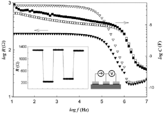
The and the observed undergo a step-like jump over a narrow range of 0.1 and 3 MHz, with the -jump occurring at higher (Fig. 1). This is similar to the Maxwell-Wagner relaxation,yu but differs from dielectric Debye relaxation.jon Carrier polarization, i.e. trapping and hopping in disordered solids,dyr appears to be a natural interpretation. In such models, only the hopping paths with all barriers contribute to the apparent conductivity , and the measures the defect distribution against the hopping barriers, , at the Fermi level. The jumps (Fig. 1), therefore, suggest a defect mesostructure with many short conducting clusters (domains) with the intra-cluster eV separated by slightly higher inter-cluster barriers, i.e. around 0.4 eV (inset, Fig. 2). It is interesting to note that the and are distinct, i.e. switchable, below 0.1–1 MHz, but the corresponding is practically the same as indicated by the Cole-Cole plot. This is very different from the samples with smaller , although both show higher after positive pulses. Also, the same above 1 MHz at both on and off states indicates a limitation on the read speed in future potential applications.
It should be pointed out that such strong dispersions of and suggest that the domain model is also in disagreement with the data. The interfacial hopping in the model has been attributed to a single barrier layer between the electrode and the proposed interfacial domain, and should therefore be -independent for . Thus, a more complicated defect network should be invoked to accommodate the dispersions. It is also interesting to note that the thermo-produced carriers can be directly deduced from the observed. The calculated value, sec-1 below 100 kHz within the interfacial layer, is far higher than the reported injected current, sec-1, at the SCLC region.bai This supports the above discussion for samples with large , and suggests that the switching mechanism can be modified through interface engineering.
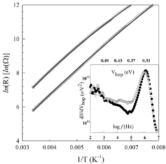
To answer the key question of why the switching can still occur, was measured at both on- and off-states (Fig. 2). While the ’s appear to be almost parallel, which makes the switching difficult to understand if , a closer examination shows that in the variable-range-hopping (VRH) formulation might be a better description, as suggested by the slight curvatures in Fig. 2. For this particular sample, the fitting parameters are (0.61) and K (8353 K) for the on (off) states, respectively. The and are traditionally associated with and DOS, where is the dimensionality.san The changes in both and , therefore, tentatively suggest that the arrangement of the defect-structures are changed. The switching, in such a case, might be more about the local structure than the average defect density.
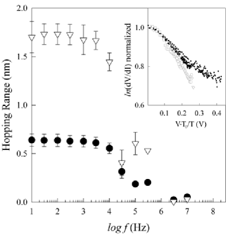
To verify this assumption, the small-signal ac at various dc biases and temperatures was measured (inset, Fig. 3). The normalized characteristics between 8 and 55 ∘C are scaled into a single trace as suggested by Mott’s formula of or ,mot where and are the hopping range and the electric field, respectively. The physical picture, i.e. the longer the hopping range, the larger the field effects will be, is straightforward and independent of the hopping details, although the absolute value may be affected by the 10 nm assumed thicknessbai of the interfacial layer. Our data, therefore, demonstrate that the hopping range is longer at the off state for MHz. It is also interesting to note the unusually small for MHz (Fig. 1, 3). This may appear only if the associated hopping barriers are negligible, which is further suggestive of local defect mesostructure. With high enough defect density, the formation of local defect-correlations becomes a means to modify the switching performance. It should be noted that, in order to accommodate the observed , the conductance may be dominated by only a few percolation paths, such that simply enhancing may not necessarily reduce the size limitations. Direct observations of such structures are called for and planned.
In conclusion, we have shown that the interfacial resistive switch found in metal-PCMO systems is a defect-mediated process. Whereas a defect density alteration occurs in samples with Hz) nF/mm2, we propose that the change in defect mesostructure may cause switching in the samples with larger . Further investigation of the parameters controlling the defect distribution will shed light on how best to proceed with the nanoscaling and benchmarking of future device applications.
Acknowledgements.
The authors thank Prof. J. Miller and Dr. N. Nawarathna for the use of and technical assistance with the impedance analyzer. The work in Houston is supported in part by NSF Grant No. DMR-9804325, the T. L. L. Temple Foundation, the John J. and Rebecca Moores Endowment, the Robert A. Welch Foundation, and the State of Texas through the Texas Center for Superconductivity at the University of Houston; and at Lawrence Berkeley Laboratory by the Director, Office of Science, Office of Basic Energy Sciences, Division of Materials Sciences and Engineering of the U.S. Department of Energy under Contract No. DE-AC03-76SF00098.References
- (1) For example, P. Weiss, Science News 167, 363 (2005).
- (2) For example, R. Waser, Resistive Switching on SrTiO3, Intel International Symposum on Resistive Switch Memory Device Benchmarking, 2005.
- (3) S. Q. Liu, N. J. Wu, and A. Ignatiev, Appl. Phys. Lett. 76, 2749 (2000).
- (4) A. Baikalov, Y. Q. Wang, B. Shen, B. Lorenz, S. Tsui, Y. Y. Sun, Y. Y. Xue, and C. W. Chu, Appl. Phys. Lett. 83, 957 (2003); S. Tsui, A. Baikalov, J. Cmaidalka, Y. Y. Sun, Y. Q. Wang, Y. Y. Xue, C. W. Chu, L. Chen, and A. J. Jacobson, Appl. Phys. Lett. 85, 317 (2004).
- (5) A. Sawa, T. Fujii, M. Kawasaki, and Y. Tokura, Appl. Phys. Lett. 85, 4073 (2004).
- (6) A. Odagawa, H. Sato, I. H. Inoue, H. Akoh, M. Kawasaki, Y. Tokura, T. Kanno, and H. Adachi, Phys. Rev. B. 70, 224403 (2004).
- (7) M. J. Rozenberg, I. H. Inoue, and M. J. Sánchez, Phys. Rev. Lett. 92, 178302 (2004).
- (8) M. J. Rozenberg, I. H. Inoue, and M. J. Sánchez, Appl. Phys. Lett. 88, 033510 (2006); M. J. Rozenberg, I. H. Inoue, and M. J. Sánchez, Thin Solid Films 486, 24 (2005); M. J. Rozenberg, I. H. Inoue, and M. J. Sánchez, cond-mat/0406646 (2004).
- (9) For example, H. Y. Hwang, S. W. Cheong, P. G. Radaelli, M. Marezio, and B. Batlogg, Phys. Rev. Lett. 75, 914 (1995).
- (10) For example, J. D. Meindl, Q. Chen, and J. A. Davis, Science 293, 2044 (2001).
- (11) For example, Z. Yu and C. Ang, J. Appl. Phys. 91, 794 (2002); P. Lunkenheimer, V. Bobnar, A. V. Pronin, A. I. Ritus, A. A. Volkov, and A. Loidl, Phys. Rev. B 66, 052105 (2002).
- (12) For example, A. K. Jonscher, IEEE Electrical Insulation Magazine 6, 16 (1990).
- (13) J. C. Dyre and T. B. Schrøder, Rev. Mod. Phys. 72, 873 (2000).
- (14) For example, B. Sanjai, A. Raghunathan, T. S. Natarajan, G. Rangarajan, S. Thomas, P. V. Prabhakaran, and S. Venkatachalam, Phys. Rev. B 55, 10734 (1997); V. I. Arkhipov, H. von Seggern, and E. V. Emelianova, Appl. Phys. Lett. 83, 5074 (2003).
- (15) N. F. Mott and E. A. Davis, Electronic Processes in Non-Crystalline Materials, 2nd ed. (Clarendon, Oxford, 1979).