Terahertz detection schemes based on sequential multi-photon absorption
Abstract
We present modeling and simulation of prototypical multi bound state quantum well infrared photodetectors and show that such a detection design may overcome the problems arising when the operation frequency is pushed down into the far infrared spectral region. In particular, after a simplified analysis on a parabolic-potential design, we propose a fully three-dimensional model based on a finite difference solution of the Boltzmann transport equation for realistic potential profiles. The performances of the proposed simulated devices are encouraging and support the idea that such design strategy may face the well-known dark-current problem.
PACS numbers: 85.35.Be, 85.60.Bt, 73.63.-b
Common quantum-well infrared photodetectors (QWIPs) are based on single-bound-state quantum wells, and electronic transitions between such bound state and the continuum are used for photon detection. QWIP Incident photons excite bound electrons into the continuum contributing to what is called the photocurrent, which is the detection signal “measured” by such devices. The well width and composition, and thus the depth of the bound state, are designed to match with the energy of the photons to be detected.
QWIPs already demonstrated as successful and reliable devices to cover the mid-infrared region of the electromagnetic spectrum. QWIP However the scaling down of the operation frequency into the terahertz range (1-10 THz) is not straightforward and still work has to be done after the first demonstration. Liu The main obstacle is the fact that at these energies (4.1-41 meV) the dark current, mainly due to the high-energy tail of the electron distribution function, may become predominant over the photocurrent signal.
The realization of THz-operating detectors, however, is a crucial milestone of strategic technological interest. High-performance quantum-cascade (QC) laser sources operating in this frequency region have, in fact, already been demonstrated. Nature The availability of reliable detection strategies is therefore the necessary step to fully access and exploit the THz-communication potential. Indeed QC designs have also been demonstrated to efficiently operate as detectors within a bound-to-bound scheme. QCLdet
In this paper we present an alternative THz-detector design which, instead of resorting on a direct bound-to-continuum transition as conventional QWIPs do, is based on a ladder of equally-spaced bound states, whose step is tuned to the target frequency of operation. This kind of photodetector is intrinsically less responsive to light than the single-bound-state system since many photons have to be absorbed to excite an electron into the continuum. However, the reduction of the dark current yields an overall better signal to noise ratio. The latter is the figure of merit we choose to characterize this device and depends on the number of bound states in the design. The latter is defined as follows
| (1) |
where is the photocurrent and the dark current. Since we are focusing on how the number of bound states may affect the system response, the relevant quantity to consider is indeed , that is, the signal to noise ratio of the system normalized to that of the single-bound-state QWIP design.
To get a first insight into the general idea of the proposed architecture, we shall start investigating a simplified strictly one-dimensional device model, i.e., a parabolic quantum well. That latter would formally produce an infinite sequence of evenly-spaced bound states along the growth direction. The key approximation is to limit our analysis to the first levels, the former being the bound states, the latter representing the continuum. The set of discrete wavefunctions is chosen to properly model the real continuum, i. e., their number is so that the electron population in the continuum is -independent. We stress that within this simplified one-dimensional model any in-plane carrier relaxation/thermalization process is necessarily treated via effective/phenomenological inter-level scattering rates. A more quantitative analysis will require a fully three-dimensional treatment of the transport problem (see below).
The evaluation of is achieved via a proper rate-equation modeling of the electron dynamics in our device which allows to access the charge population of the generic -th level. At this level of description, we may simply assume that the currents are proportional to the charge density in the continuum and thus redefine as
| (2) |
where the superscripts again refer to the contribution due to the radiation to be detected (ph) or to the dark current component (dark). The electron-photon dipole matrix element for in-plane propagating radiation is exactly known for a parabolic potential profile and textbook formulas have been used to model the effect of light in the first levels. Messiah In the model, the continuum levels do not interact with light as it would be in a real continuum.
The charge populations for a fixed configuration have been derived solving a set of steady-state rate equations of the form
| (3) |
where is the total, i.e. summed over all interaction mechanisms (electron-phonon, electron-electron, etc.), scattering rate from state to state . The contribution to the latter due to non-optical interactions, , may be expressed in terms of a phenomenological lifetime , independent on the level index. In particular, is such to achieve thermodynamic equilibrium in the absence of light according to
| (4) |
when (decay) and
| (5) |
when (excitation).
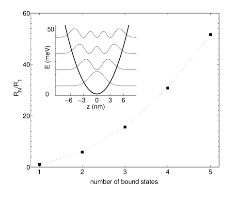
Figure 1 shows the simulated ratio, as a function of , for the parabolic potential profile sketched in the inset and with a lifetime ps. The operation frequency is 3 THz and the optical power is set in the linear response regime of the device. The results demonstrate that increases with the number of bound states thus suggesting that the proposed detection scheme actually improves the response with respect to the single-bound-state QWIP.
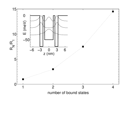
Actually, a key-feature of the above parabolic-potential model is the fact that optical dipole matrix elements increase with the quantum number, thus intrinsically improving the response as long as more bound states are considered. This is certainly not the case for a real potential profile and the feasibility of our architecture has to be tested on more realistic designs. In particular, the realistic potential profile of choice in our fully three-dimensional analysis is a triple quantum well with a wide central well defining the number of bound states and two thin lateral wells whose dimensions are tailored to tune the inter-level spacings. This profile can be seen in the inset of figure 2.
To get a more refined modeling of the carrier dynamics in our heterostructure, taking into account the three-dimensional nature of the problem, we adopt a kinetic Boltzmann-like approach. The fundamental ingredient of the latter is the carrier distribution function which represents the occupation probability of a single-particle state with in-plane wavevector k in the -th subband. The time evolution of is governed by the following transport equation:
| (6) |
where is an external static electric field and is the scattering probability for a process connecting the state with in-plane wavevector k in the -th subband to the state k’ in the -th one.
The 3D single-particle electron states forming the basis set of our scattering dynamics are obtained within the standard envelope-function approximation, using a plane-wave expansion strategy as described in Ref. BBR, . Dipole matrix elements are then numerically evaluated while, at this preliminary level of description, other scattering processes are still modeled in terms of a phenomenological lifetime. The carrier dynamics then results from a finite-difference solution of the above Boltzmann transport equation, in cylindrical coordinates with the polar plane parallel to the growth direction. In particular, our time-step procedure starts from a known distribution function, evaluates its variations over a certain time interval and then uses the new value as the starting point for the forthcoming step.
The simulation is carried out applying a static electric field V/cm along the growth direction and then evaluating the current with and without incident light. The signal-to-noise ratio is then estimated according to Eq. (2) and its values are plotted in figure 2 as a function of the number of bound states . Our prototypical device is tuned to operate at 3.3 THz, an electron mean lifetime ps is assumed and the incident power is kept within the linear response regime. The graph shows that grows super-linearly with the number of bound states , thus confirming the earlier results obtained with the simplified parabolic-potential model.
This occurs in spite of the fact that the potential profile sketched in the inset of figure 2 is not the best choice to optimize the electron-photon interaction. The latter depends on the overlap integral between the wavefunctions of the initial and final states of the transition and a proper device design is crucial, in this respect, for the overall response of the photodetector. However, at this level of analysis, we focused on achieving an evenly-spaced set of bound states, since our aim was to verify whether a multi-photon absorbtion scheme could improve the detector responsivity over the single bound state design. The issue of optimizing the device performance in such a novel architecture will be addressed in a second stage.
To summarize, we have presented a novel QWIP architecture to face the dark current related problems that affect more conventional designs especially when the device is operating above cryogenic temperatures. Our results demonstrate that a multi-bound-state QWIP structure can significantly improve the signal-to-noise ratio, thus yielding better results as the number of bound states is increased. Several aspects, both in the design and the modeling, deserve a more refined analysis for a quantitative evaluation and optimization of device performances. These include, for example, a microscopic description of the relevant scattering processes (e.g., carrier-phonon), a more optically efficient potential profile and then simulations of a real device with its physical boundaries (contacts).
References
- (1) See. e. g., H. C. Liu, in Intersubband Transitions in Quantum Wells: Physics and Device Applications I, Semiconductors and Semimetals, Vol. 62, edited by H. C. Liu and F. Capasso (Academic, San Diego, 2000), Chap. 3, pp. 126-196.
- (2) H. C. Liu et al., Appl. Phys. Lett. 84, 4068 (2004).
- (3) R. Köhler et al., Nature 417, 156 (2002).
- (4) M. Graf et al., Appl. Phys. Lett. 84, 475 (2004).
- (5) A. Messiah, Quantum Mechanics (North-Holland, Amsterdam, 1985).
- (6) S. Barbieri, F. Beltram, F. Rossi, Phys. Rev. B, 60, 1953 (1999).