Peculiar Width Dependence of the Electronic Property of Carbon Nanoribbons
Abstract
Nanoribbons (nanographite ribbons) are carbon systems analogous to carbon nanotubes. We characterize a wide class of nanoribbons by a set of two integers , and then define the width in terms of and . Electronic properties are explored for this class of nanoribbons. Zigzag (armchair) nanoribbons have similar electronic properties to armchair (zigzag) nanotubes. The band gap structure of nanoribbons exhibits a valley structure with stream-like sequences of metallic or almost metallic nanoribbons. These sequences correspond to equi-width curves indexed by . We reveal a peculiar dependence of the electronic property of nanoribbons on the width .
I Introduction
Nanometric carbon materials exhibit various remarkable properties depending on their geometryDresselhaus ; Kroto ; Iijima ; Hamada ; Appl ; Mintmire ; Wildoer ; Jorio ; Shima ; Saito ; Ouyang . In particular, intensive research has been made on carbon nanotubesIijima in the last decade. Carbon nanotubes are obtained by wrapping a graphene sheet into a cylinder form. The large interest centers their peculiar electronic properties inherent to quasi-one-dimensional systems.
A similarly fascinating carbon system is a stripe of a graphene sheet named nanographite ribbons, graphene ribbon or nanographeneKivelson ; Tanaka ; Dunlap ; Fujita ; Ajiki ; Wakaba ; Ryu ; Duplock . We call them carbon nanoribbons in comparison with carbon nanotubes. They can be manufactured by deposition of nanotubes or diamondsMurakami ; Zhang ; Shibayama ; Affoune . Experimental studies have begun only recentlyCancado ; Niimi ; Kobayashi ; Matsui . Nanoribbons have a higher variety than nanotubes because of the existence of edges. Wide nanoribbons with zigzag edges have been argued to possess the flat band and show edge ferromagnetismFujita . Though quite attractive materials, their too rich variety has made it difficult to carry out a systematic analysis of carbon nanoribbons.
In this paper we make a new proposal to characterize a wide class of nanoribbons by a set of two integers representing edge shape and width. The width is defined in terms of and . We present a systematic analysis of their electronic property in parallel to that of nanotubes. Carbon nanotubes are regarded as a periodic-boudary-condition problem while carbon nanoribbons are as a fixed-boudary-condition problem. By calculating band gaps they are shown to exhibit a variety of properties in electronic conduction, from metals to typical semiconductors. Several sequences of metallic or almost metallic (MAM) points are found in the valley of semiconducting nanoribbons. We reveal a peculiar dependence of the electronic property of nanoribbons on the width . For instance, these sequences and equi-width curves become almost identical for wide nanoribbons. We also point out that the distribution of van-Hove singularities as a function of shows a peculiar stripe pattern.
This paper is composed as follows. In section II we characterize a wide class of nanoribbons by a set of two integers and introduce the width . In section III, making a numerical study, we present an overview of the band gap structure for this class of nanoribbons. In section IV we compare nanoribbons with nanotubes. Zigzag nanoribbons, being indexed by with even , correspond to armchair nanotubes; armchair nanoribbons, indexed by with odd , correspond to zigzag nanotubes. In section V we discuss sequences of metallic points developed in the valley of semiconducting nanoribbons, where the metallic points on the principal sequence are derived analytically. In section VI we analyze sequences of MAM points more in detail. The -th sequence starts from the metallic armchair nanotube . It approaches the equi-width curve with for wide nanoribbons. In section VII we discuss edge effects. We take into account them in three ways: the nonuniform site energy, the nonuniform transfer energy and the band filling factor.
II Classification of Carbon Nanoribbons
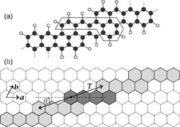
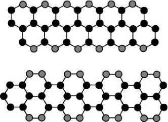
A carbon nanoribbon is a one-dimensional aromatic compound. We have illustrated a typical structure in Fig.1(a). It consists of carbon atoms of a honeycomb structure. A carbon on the edge is terminated by a different atom such as a hydrogen so that it has no dangling bond. All carbon atoms are connected by bonds between sp2 hybridized orbitals of 2s, 2px and 2py, providing with a framework of honeycomb lattice. On the other hand, the bond is formed between two 2pz orbitals. The bands cross the Fermi energy, while the bands are far away from it. Hence it is a good approximation to take into account only electrons to investigate electronic properties of nanoribbons. Each carbon atom has the complete shell and there is one electron per atom.
Embedding them into a honeycomb lattice [Fig.1(b)], we classify nanoribbons as follows. An arbitrary lattice point on a honeycomb lattice is described by the lattice vector
| (1) |
where and are primitive lattice vectors while and are integers [Fig.1(b)]. First we take a basic chain of connected carbon hexagons, as depicted in dark gray. Second we translate this chain by the translational vector
| (2) |
as depicted in light gray, where is an arbitrary integer . Repeating this translation many times we construct a nanoribbon indexed by a set of two integers , where . In what follows we analyze the class of nanoribbons generated in this way.
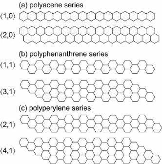
The indices and specify the type of nanoribbons. The case with represents a zigzag nanoribbon with zigzag edge, while the case with represents an armchair nanoribbon with armchair edge. The nanoribbons with , and are known as polyacene, polyphenanthrene and polyperynaphthaleneKivelson ; Tanaka ; Murakami ; Yudasaka ; Affoune , respectively [Fig.2].
We propose to define the width of the nanoribbon by
| (3) |
where is the angle between the basic chain and the translational vector,
| (4) |
as in Fig.1(b). There is a freedom to normalized the width. We have normalized the width of an armchair nanoribbon indexed by to be
| (5) |
by the reason that becomes clear in Section VI. Then, the width of zigzag nanoribbons indexed by becomes
| (6) |
The width of a nanoribbon corresponds to the diameter of a nanotube. Though a nanoribbon is specified by two integers, we expect that the electronic property of wide nanoribbons is mainly controlled by the width .
The above classification rule is similar to that of nanotubes based on the chiral vector or the rolling up vectorSaito ; Ouyang ; Seifert2 , but it is clearly different since some nanoribbons can not be rolled up into nanotubes. We discuss the correspondence between nanoribbons and nanotubes in Section IV.
III Electronic structure of nanoribbons
We calculate the band structure of nanoribbons based on the nearest-neighbor tight-binding model, which has been successfully applied to the studies of carbon nanotubesSaito .
The tight-binding Hamiltonian is defined by
| (7) |
where is the site energy, is the transfer energy, and is the creation operator of the electron at the site . The summation is taken over the nearest neighbor sites . In the case of nanotubes, constant values are taken for and owing to their homogeneous geometrical configuration. Furthermore, since there exists one electron per one carbon, the band-filling factor is 1/2. In the case of nanoribbons, on the contrary, they would be modified by the existence of the edges. (a) The site energy would be modified by the difference of electronegativity of X, where X represents a different atom such as hydrogen. (b) The transfer energy would be modified by a possible lattice distortion near the edge. (c) The band-filling factor would be modified due to the dipole moment of C-X bonds. It is our basic assumption that the carbon nanoribbon can be analyzed based on this Hamiltonian together with these three modifications.
It is convenient to take a unit cell as shown in Fig.1(a). There are carbon atoms in a unit cell of the nanoribbon indexed by , as implies that the proper functions of the Hamiltonian consist of Bloch wave functions . We take overlap integrals as
| (8) |
where is Kronecker’s delta. The bands of nanoribbon are derived from the Hamiltonian with the crystal momentum, which is a matrix. The band structure is determined by
| (9) |
where is a unit matrix due to the overlap integral.
Though the nanoribbon may have different values of and for atoms on the edge from the others, as we have remarked, the difference is expected to be quite small. We first neglect the difference. Namely, we take the transfer energy to be between all the nearest neighbor sites and otherwise to be . It is generally takenSaito as eV. We also neglect the site energy term in the Hamiltonian (7) by taking all the site energy equal. We discuss how the gap structure is modified by edge corrections in Section VII.
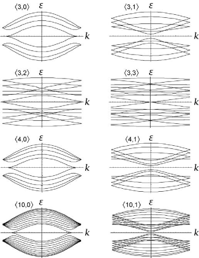
We have solved the eigenvalue problem (9) numerically for . Typical band structures are shown in Fig. 3. As is seen in the figures, band structures depend strongly on the parity of , but only weakly on . We also find the following: (a) For metallic nanoribbons, the Fermi point of even is at , and that of odd is at . (b) For semiconducting nanoribbons, the band gap minimum of even is at , and that of odd is at .
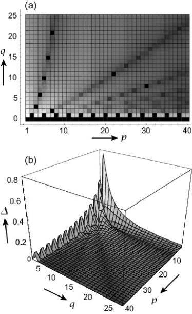
As a main result we display an overview of the band gap structure of nanoribbons in Fig. 4. Gapless states (represented by black squares) are metallic, and gapfull states (represented by all other squares) are semiconducting. There are a variety of semiconducting nanoribbons from almost gapless ones (represented by dark gray squares) to large gapfull ones (represented by light gray squares). We observe clearly three emergence patterns of metallic points: (a) Metallic points for all . (b) Metallic points with . (c) Several sequences of metallic points on "streams" in valleys. We discuss (a) and (b) in Section IV, and (c) in Sections V and VI.
IV Nanoribbons versus Nanotubes
It is observed that nanoribbons indexed by are metallic for all , which are in the polyacene series with zigzag edges [Fig. 2(a)]. Nanoribbons indexed by with are found to be also metallic, which have armchair edges [Fig. 2(b) and (c)]. This series has period , as is a reminiscence of the classification rules familiar for nanotubes. The classification rule says that a nanotube is metallic when is an integer multiple of , and otherwise semiconducting, where is a chiral vector of the nanotube.
Let us explore the correspondences more in detail. There is a group of nanoribbons each of which is constructed as a development of a nanotube by cutting it along the translational vector. For example, a zigzag nanoribbon with even may be regarded as a development of the armchair nanotube whose chiral vector is . All zigzag nanoribbons are metallic, as corresponds to the fact that all armchair nanotubes are metallic. As another example, an armchair nanoribbon with odd may be regarded as a development of a zigzag nanotube whose chiral vector is . Armchair nanoribbons are metallic with period of , as corresponds to the fact that metallic zigzag nanotubes emerge by period of .
The correspondence between these metallic points may be explained by the absence of spiral currents in carbon nanotubes. Namely, currents flowing along the axis of nanotubes are not affected by cutting along the axis. There is no direct correspondence between chiral nanotubes and nanoribbons for .
V Sequence of metallic Nanoribbons
It is remarkable that there are new series of discrete metallic points on one-dimensional curves in Fig.4. These curves look like streams in valleys. The prominent ones are at , , , , , , . We regard them to form the principal sequence of metallic points of nanoribbons. There are also sequences of metallic points on higher curves.
We are able to derive the principal sequence analytically. We start with the observation that the density of states at the Fermi energy is , if the band structure of nanoribbons are gapless; otherwise, . This follows from the reflection symmetry around and the existence of one electron per one atom. The reflection symmetry is due to a bipartite lattice structure of graphiteLieb . Consequently, to investigate the metallic points, it is enough to analyze
| (10) |
We have if this equation has a solution, and the nanoribbon is gapless; otherwise it is gapfull. We find simple structures at and for .
At , the determinant (10) is explicitly calculated as
| (11) |
It vanishes for any at . Because of this, every zigzag nanoribbon is metallic. It follows that
| (12) |
We have thus verified analytically that the flat band emerges for when the width of nanoribbons is wide enough, as confirms a previous numerical resultFujita , where the flat band has been argued to lead to edge ferromagnetism.
For and with integer , the determinant (10) has a factor such that
| (13) |
and the nanoribbon is found to be gapless at .
For , the determinant (10) is calculated as
| (14) |
We can prove that for a certain provided that
| (15) |
Nanoribbons are metallic on the points with integers and with (15). They constitute the principal sequence of metallic points.
It is hard to solve analytically for , though the existence of solutions is clear by numerical analysis as in Fig.4(a). In this figure there are only three metallic points; the two points are and on the second sequence, and the last point is on the third sequence.
Metallic points on higher sequences are quite curious in this respect. We cannot tell how they arise systematically. However, it may be useless to make efforts to distinguish between metallic and tiny-gap semiconductor too seriously, since the simple tight-binding model we have used will not be accurate enough to predict completely vanishing band gaps. Nevertheless the valley structure with several "streams" will be a significant feature. Hence it is more interesting how the sequences made of MAM (metallic or almost metallic) points are located in valleys.
VI Width-Dependence of Nanoribbons
We have defined the width of a nanoribbon by the formula (3). We now argue that the sequences of MAM points are indexed by this width.
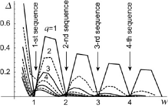
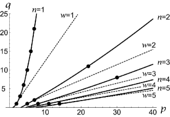
First, in Fig.5 we have depicted the band gap as a function of the width for each fixed value of . The band gap behaves inversely to . This reminds us that the band gap of a carbon nanotube is inverse proportion to the radius. The characteristic feature is that all band gaps with different take local minima almost at the same values of width , . It indicates that nanoribbons with similar width share qualitatively the same electronic property. The first local minimum corresponds to the principal sequence, which may be regarded as an extension of the armchair nanoribbon indexed by . In the same way the -th sequence may be regarded as an extension of the armchair nanoribbon with .
Solving eq.(3) for , we have
| (16) |
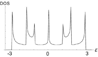
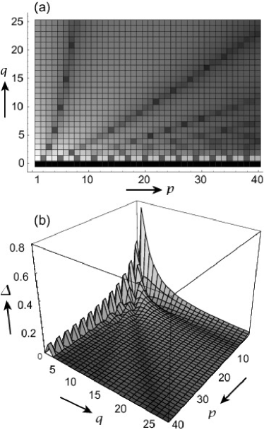
In Fig.6 we show the curves described by this equation and the sequences of MAM points. It is observed that the -th sequence is almost tangent to the equi-width curve with at . We are able to associate the sequences with the equi-width curves in this way. These two curves become almost identical for sufficiently wide nanoribbons. This result may be understood as follows. In the case of a continuous ribbon with no lattice structure, the only parameter is the width and the electronic property is determined by this parameter. We present another indication that the width is an interesting parameter. We calculate the density of state of an arbitrary nanoribbon numerically [Fig.7]. There are many van-Hove singularities just as in nanotubes because nanoribbons are also one-dimensional compounds. The global structure of the density of state is determined by van-Hove singularities. These peaks can be measured experimentally by Raman scatteringJorio ; Rao ; Cancado ; Kim .
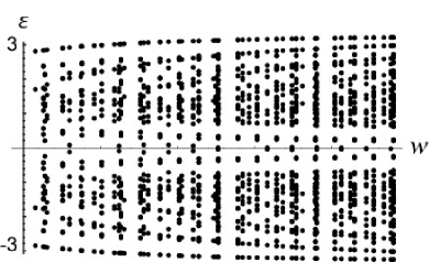
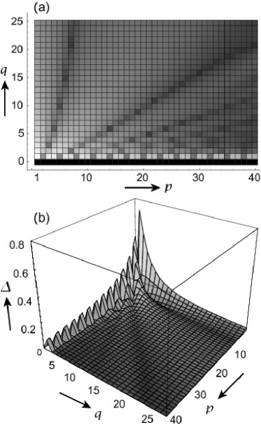
We calculate the energies at which van-Hove singularities develop due to the local band flatness at for various nanoribbons. Note that the optical absorption is dominant at because the dispersion relation with the light velocity. On the other hand the width is determined by and as in (3). We show the energy of this peak as a function of in Fig.8. A peculiar stripe pattern is manifest there. In particular, the maximum and minimum values take almost the same values , reflecting the electronic property of a graphiteSaito . The fact that there are on smooth curves justify a physical meaning of the width . This stripe pattern would be accessible experimentally by way of Raman scattering.
VII Edge corrections
We finally study how the gap structure is modified by the existence of edges in a carbon nanoribbon. All carbon atoms in a carbon nanotube are equivalent in the sense that each of them is always surrounded by three carbon atoms. In contrast, this is not the case for a nanoribbon, where a carbon on the edge has less neighboring carbon atoms. The presence of C-X bonds introduces carbon atoms on edge with a different nature. We assume that the edge effects can be taken into account by modifying the band-filling factor, the transfer energy and the site-energy in the Hamiltonian (7). We take and for those associated with edge carbons, and and for bulk carbons [Fig.9].
First, the band-filling factor is affected by the dipole moment of C-X bonds. The change of electron number is given at most by the number of C-X bonds and is small for wide nanoribbons. This effect does not modify the band structure, but only changes the occupancy of the band. As a result, semiconducting nanoribbons tend to become metallic nanoribbons.
Second, the transfer energy is affected by the change of the distance between two carbons near the edge. The distortion does not break the inversion symmetry of the band structure. Recalculating the band structure of various nanoribbons, we have found that the difference is hardly recognizable. We show the band structure of the nanoribbon in Fig.10, assuming a large correction such that to make the difference recognizable.
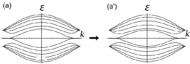
Finally, the site energy is affected by the difference of electronegativity of X. The effect is expected to be also very small because the site energy of electrons is mainly determined by carbon atoms. It breaks the inversion symmetry because the lattice of carbon atoms cannot be resolved into two sublattices any moreLieb . For this reason the Fermi energy is moved from . The recalculated band structure of zigzag and armchair nanoribbons is given by assuming a large choice of the edge correction, , in Fig.11. The modification is small as expected, though some of metallic armchair nanoribbons become semiconducting.
In general the transfer-energy correction must be smaller than the site-energy correction because the former is due to a structural distortion while the latter is due to the electronegativity. The transfer-energy correction will be negative by considering the expansion effect near the surface. On the other hand, the site-energy correction will be positive or negative if the relative electronegativity of the edge atoms is positive or negative.
We present an overview of the band gap structure of various nanoribbons with the edge corrections by making a choice of and in Fig.12, and by making a choice of and in Fig.13. Comparing them with Fig.4, some features of edge effects are manifest: (A) The valley structure with stream-like sequences remains as they are. (B) All zigzag nanoribbons remains gapless. (C) Armchair nanoribbons are most strongly affected. (D) Edge effects are negligible for wide nanoribbons.
VIII Discussion
We have systematically studied and presented a gross view of the electronic property for a wide class of carbon nanoribbons. They exhibit a rich variety of band gaps, from metals to typical semiconductors. Zigzag and armchair nanoribbons have electronic properties similar to nanotubes, but other nanoribbons are quite different. It is remarkable that there exist sequences of metallic or almost metallic nanoribbons which look like streams in valley made of semiconductors. They approach equi-width curves for wide nanoribbons. We have revealed a peculiar dependence of the electronic property of nanoribbons on the width . These characteristic features are not affected strongly by edge corrections even for narrow nanoribbons.
In our analysis we have employed the nearest-neighbor tight-binding model. It is worthwhile to calculate band gaps by more rigorous methods such as a density-functional theoryPorezag ; Kusakabe ; Maruyama ; Higuchi . It is interesting to examine whether metallic points on the sequences we have discovered remain gapless in these calculations. We also note that edge corrections have been calculated by a tight binding density-functional method in several cases for other materialsLee ; Seifert ; Hajnal ; Seifert3 ; Kohler . Needless to say it is an extremely hard task to carry out these calculations and practically impossible to make a systematic analysis based on them. Our results on the electronic property of carbon nanoribbons will be useful as a guidepost for those advanced studies.
In passing, we remark that experimental studies of nanoribbons are just in the beginning stageCancado ; Niimi ; Kobayashi in comparison with the study of nanotubes. This may be due to a difficulty of manufacturing and selecting good samples, but the recent technical developing will soon solve this problem. The band gap study of various nanoribbons presented in this paper may be a basic step for various application of carbon nanoribbons.
The author is very thankful to Professors H. Aoki and R. Saito for various stimulating discussions.
References
- (1) M. S. Dresselhaus, G. Dresselhaus, K. Sugihara, I. L. Spain and H. A. Goldberg, Graphite Fibers and Filaments, Springer Series in Material Science Vol 5 (Springer-Verlag, Berlin, 1988).
- (2) H. W. Kroto, J. R. Heath, S. C. O’Brien, R. F. Curl, R. E. Smalley, Nature (London) 318, 167 (1985).
- (3) S. Iijima, Nature (London) 354, 56 (1991).
- (4) N. Hamada, S. I. Sawada, and A. Oshiyama, Phys. Rev. Lett. 68, 1579 (1992).
- (5) R. Saito, M. Fujita, G. Dresselhaus, and M. S. Dresselhaus, Appl. Phys. Lett. 60 18 (1992).
- (6) J. W. Mintmire, B. I. Dunlap, and C. T. White, Phys. Rev. Lett. 68, 631 (1992).
- (7) A. Jorio, R. Saito, J. H. Hafner, C. M. Lieber, M. Hunter, T. McClure, G. Dresselhaus, and M. S. Dresselhaus, Phys. Rev. Lett. 86, 1118 (2001).
- (8) N. Shima, and H. Aoki, Phys. Rev. Lett. 71, 4389 (1993).
- (9) J. W. G. Wildöer, L. C. Venema, A. G. Rinzler, R. E. Smalley, and C. Dekker, Nature (London) 391, 59 (1998).
- (10) R. Saito, G. Dresselhaus, and M. S. Dresselhaus, Physical Properties of Carbon Nanotubes, Imperial College Press, 1998, London.
- (11) M. Ouyang, J. L. Huang, C. M. Lieber, Ann. Rev. Phys. Chem 53 (2002) 201.
- (12) S. Kivelson and O. L. Chapman, Phys. Rev. B 28, 7236 (1983).
- (13) K. Tanaka, K. Ohzeki, S. Nankai, T. Yamabe, H. Shirakawa, J. Phys. Chem. Solids 44, 1069 (1983).
- (14) B. I. Dunlap, Phys. Rev. B 49, 5643 (1994).
- (15) M. Fujita, K. Wakabayashi, K. Nakada, and K. Kusakabe, J. Phys. Soc. Jpn. 65, 1920 (1996).
- (16) K. Wakabayashi, M. Fujita, H. Ajiki, and M. Sigrist Phys. Rev. B 59 8271 (1999).
- (17) K. Wakabayashi, and M. Sigrist, Phys. Rev. Lett. 84, 3390 (2000).
- (18) S. Ryu, and Y. Hatsugai, Phys. Rev. B 67, 165410 (2003).
- (19) E. J. Duplock, M. Scheffler, P. J. D.Lindan, Phys. Rev. Lett. 92 225502 (2004).
- (20) M. Murakami, S. Iijima, and S. Yoshimura, J. Appl. Phys. 60, 3856 (1986).
- (21) M. Zhang, D. H. Wu, C. L. Xu, and W. K. Wang, Nanostruct. Matter. 10, 1145 (1998).
- (22) Y. Shibayama, H. Sato, T. Enoki, and M. Endo, Phys. Rev. Lett. 84 1744 (2000).
- (23) A. M. Affoune, B. L. V. Prasad, H. Sato, T. Enoki, Y. Kaburagi, and Y. Hishoyama, Chem. Phys. Lett. 348, 17 (2001).
- (24) L. G. Cancado, M. A. Pimenta, B. R. A Neves, G. Medeiros-Ribeiro, T. Enoki, Y. Kobayashi, K. Takai, K. I. Fukui, M. S. Dresselhaus, R. Saito, and A. Jorio, Phys. Rev. Lett, 93 047403 (2004).
- (25) Y. Niimi, T. Matsui, H. Kambara, K. Tagami, M. Tsukada, and H. Fukuyama. Appl. Surf. Sci. 241, 43 (2005).
- (26) Y. Kobayashi, K. Fukui, T. Enoki, K. Kusakabe, and Y. Kaburagi, Phys. Rev. B, 71 193406 (2005).
- (27) T. Matsui, H. Kambara, Y. Niimi, K. Tagami, and H. Fukuyama, Phys. Rev. Lett. 94,226403 (2005).
- (28) M. Yudasaka, Y. Tasaka, M. Tanaka, H. Kamo, Y. Ohki, S. Usami, and S. Yoshimura, Appl. Phys. Lett. 64,3237 (1994).
- (29) G. Seifert, H. Terrones, M. Terrones, G. Jungnickel, and Th. Frauenheim, Phys. Rev. Lett. 85 (2000) 146.
- (30) E. H. Lieb, Phys. Rev. Lett. 62, 1201 (1989).
- (31) A. M. Rao, A. Jorio, M. A. Pimenta, M. S. S. Dantas, R. Saito, G. Dresselhaus, and M. S. Dresselhaus, Phys. Rev. Lett. 84 1820 (2000).
- (32) P. Kim, T. W. Odom, J.-L. Huang and C. M. Lieber, Phys. Rev. Lett. 82 (1999) 1225.
- (33) D. Porezag, Th. Frauenheim, Th. Köhler, G. Seifert and R. Kaschner, Phys. Rev. B 51 (1995) 12947.
- (34) K. Kusakabe and M. Maruyama, Phys. Rev. B, 67 (2003) 092406.
- (35) M. Maruyama, K. Kusakabe, S. Tsuneyuki, K. Akagi, Y. Yoshimoto and J. Yamauchi, J. Phys. Chem. Solids, 65 (2004) 119.
- (36) Y. Higuchi, K. Kusakabe, N. Suzuki, S. Tsuneyuki, J. Yamauchi, K. Akagi, Y. Yoshimoto, J. Phys. Cond. Matt. 16 (2004) S5689.
- (37) G. Seifert, Th. Frauenheim, T. Köhler, et al. Phys. Stat. Solid B. 225 (2001) 393.
- (38) Th. Köhler, Th Frauenheim, Z. Hajnal and G. Seifert, Phys. Rev. B 69 (2004) 193403.
- (39) S. M. Lee, M. A. Belkhir, X. Y. Zhu, Y. H. Lee, Y. G. Hwang and Th. Frauenheim. Phys. Rev. B 61 (2000) 16033.
- (40) Z. Hajnal, G. Vogg, L. J. -P. Meyer, B. Szücs, M. S. Brandt, and Th. Frauenheim, Phys. Rev. B 64 (2001) 033311.
- (41) G. Seifert , T. Köhler, H. M. Urbassek, E. Hernández, and Th. Frauenheim, Phys. Rev. B 63 (2001) 193409.