Photo-assisted Andreev reflection as a probe of quantum noise
Abstract
Andreev reflection, which corresponds to the tunneling of two electrons from a metallic lead to a superconductor lead as a Cooper pair (or vice versa), can be exploited to measure high frequency noise. A detector is proposed, which consists of a normal lead–superconductor circuit, which is capacitively coupled to a mesoscopic circuit where noise is to be measured. We discuss two detector circuits: a single normal metal – superconductor tunnel junction and a normal metal separated from a superconductor by a quantum dot operating in the Coulomb blockade regime. A substantial DC current flows in the detector circuit when an appropriate photon is provided or absorbed by the mesoscopic circuit, which plays the role of an environment for the junction to which it couples. Results for the current can be cast in all cases in the form of a frequency integral of the excess noise of the environment weighted by a kernel which is specific to the transport process (quasiparticle tunneling, Andreev reflection,…) which is considered. We apply these ideas to the measurement of the excess noise of a quantum point contact and we provide numerical estimates of the detector current.
I Introduction
Over the last decades, the measurement of noise has become a widely accepted diagnosis in the study of electronic quantum transportyang ; blanter_buttiker ; chamon_freed96 . Indeed, noise provides information on the charge of the carriers in unconventional conductors, when considering the Fano factor – the ratio of the noise to the average current – in the regime where the carriers tunnel independently. Away from this Poissonian regime, noise also contains crucial information on the statistics of the charge carriers martin_landauer . Experimentally, low frequency noise in the kHz–MHz range is more accessible than high frequency (GHz–THz) noise: it can in principle be measured using state of the art time acquisition techniques. For higher frequency measurements, it is becoming necessary to build a noise detector on chip for a specific range of high frequencies. In this work we consider a detector circuit which is capacitively coupled to the mesoscopic device. This circuit is composed of a normal metal – superconductor junction (NS junction). Transport in this circuit occurs when the electrons tunneling between the normal metal and the superconductor are either tunneling elastically, or when they are able to gain or to loose energy via photo-assisted Andreev reflections. The “photon” is provided or absorbed from the mesoscopic circuit which is capacitively coupled to the NS detector. The measurement of a DC current in the detector can thus provide information on the absorption and on the emission component of the current noise correlator.
Several theoretical efforts have been made to describe the high frequency noise measurement process lesovik_loosen . This is motivated by the fact that in specific transport setups, high frequency noise detection is required in order to fully characterize transport. Examples are Bell inequality tests chtchelkatchev ; lebedev_lesovik_blatter and the detection of the anomalous charges in one dimensional correlated systemslebedev_crepieux_martin ; dolcini . The former require information about high frequency noise in order to establish a correspondence between electron number correlators and current noise correlators. The latter requires a high frequency noise measurement in order to obtain a non-zero signal when the nanotube is connected to Fermi liquid leads, which tend to wash out the features of a one dimensional correlated electron system.
In Ref. aguado_kouwenhoven, , a detection circuit, which was capacitively coupled to the mesoscopic circuit to be measured, was proposed as a high frequency noise detector. This interesting theoretical idea has so far eluded experimental verification, possibly because in the double dot system, additional (unwanted) sources of inelastic scattering render a precise noise measurement quite difficult. It is therefore necessary to look for detection circuits which are less vulnerable to dissipation, as is the case of superconducting circuits, because of the presence of the superconducting gap. Indeed, the basic idea of Ref. aguado_kouwenhoven, was implemented experimentally recentlydeblock1 ; deblock2 using a superconductor – insulator – superconductor (SIS) junction as a detector, measuring in this case the finite frequency noise characteristics of a Josephson junction.
More recently, the noise of a carbon nanotube/quantum dot was also measured onac using capacitive coupling to an SIS detector, with the detection of Super-Poissonian noise resulting from inelastic cotunneling processes. The latter proposals, together with their successful experimental implementations, indicate that superconducting detector circuits have advantages over normal detection circuits because of the presence of the superconducting gap.

The purpose of the present work is thus to analyze a similar situation, except that the SIS junction is replaced by an NS circuit which transfers two electrons using Andreev reflection between a normal lead and a superconductor. The present scheme is similar in spirit to the initial proposal of Ref. aguado_kouwenhoven, , in the sense that it exploits dynamical Coulomb blockade physics ingold_nazarov . However, here two electrons need to be transferred from / to the superconductor, and such transitions involve high lying virtual states which are less prone to dissipation because of the superconducting gap, similarly to the SIS detector of Refs. deblock1, ; deblock2, ; onac, . Andreev reflectionbtk typically assumes a good contact between a normal metal and a superconductor, but in general it can be applied to tunneling contacts – it then involves tunneling transitions via virtual states. Consequently, depending on the applied DC bias, two successive “inelastic” electron jumps are required for a current to pass through the measurement circuit. The amplitude of the DC current as a function of bias voltage in the measurement circuit provides an effective readout of the noise power to be measured.
I.1 Detector consisting of a single NS junction
The detector circuit is depicted in Fig. 1. Two capacitors are placed, respectively, between each side of the mesoscopic device and each side of the NS tunnel junction. This means that a current fluctuation in the mesoscopic device generates, via the capacitors, a voltage fluctuation across the NS junction. In turn, the voltage fluctuations translate into fluctuations of the phase around the junction. The presence of the neighboring mesoscopic circuit acts as a specific electromagnetic environment for this tunnel junction, which is described in the context of dynamical Coulomb blockadeingold_nazarov for this reason.
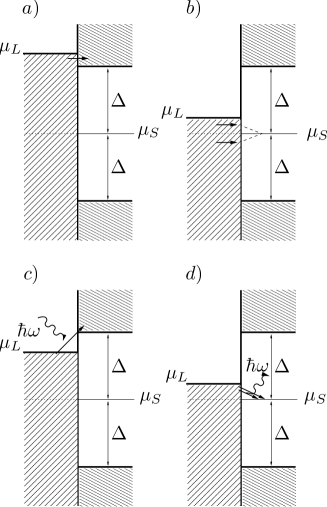
Fig. 2 depicts several scenarios for transport through an NS interface. Elastic transfer of single electrons can occur if the voltage applied to the junction is larger than the gap (Fig. 2a). Below the gap, elastic transport can only occur via Andreev reflection btk , effectively transferring two electrons with opposite energies with respect to the superconductor chemical potential (Fig. 2b). Single electron can be transferred with an initial energy below the gap, provided that a “photon” is provided from the environment in order to create a quasiparticle in the superconductor (Fig. 2c). Similarly, Andreev reflection can be rendered inelastic by the environment: for instance, two electrons on the normal side, with total energy above the superconductor chemical potential, can give away a “photon” to the environment, so that they can be absorbed as a Cooper pair in the superconductor (Fig. 2d). As we shall see, such inelastic Andreev processes are particularly useful for noise detection.
I.2 Detector consisting of an NS junction separated by a quantum dot
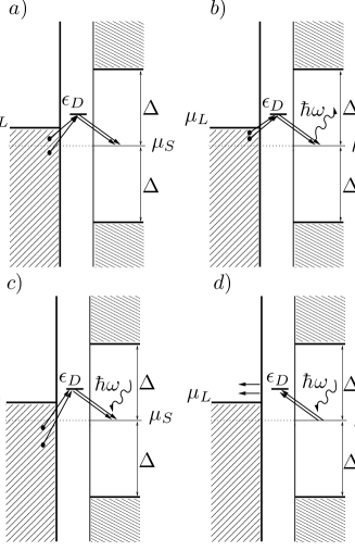
After studying the noise detection of the single NS junction, we will turn later on to a double junction consisting of a normal metal lead, a quantum dot operating in the Coulomb blockade regime, and a superconductor connected to the latter (Fig. 3). The charging energy of the dot is assumed to be large enough that double occupancy is prohibited. This setup has the advantage on the previous proposal that additional energy filtering is provided by the quantum dot. Below, we refer to this system as the normal metal–dot–superconductor (NDS) detector circuit.

In Fig. 4, the quantum dot level is located above the superconductor chemical potential, and placed well within the gap in order to avoid quasiparticle processes. Because double occupancy is prohibited by the Coulomb blockade, Andreev transport occurs via sequential tunneling of the two electrons. Yet, because of energy conservation, the same energy requirements as in Fig. 2b have to be satisfied for the final states (electrons with opposite energies, see Fig. 4a). In T-matrix terminology, for this transition to occur, virtual states corresponding to the energy of the dot are required, which suppress the Andreev tunneling current because of large energy denominators in the transition rate. Figs. 4 b, c, d, describe the cases where an environment is coupled to the same NDS circuit. Provided that this environment can yield or give some of its energy to the NDS detector, electronic transitions via the dot can become much more likely because electron energies on the normal side can be close to that of the dot level. Such transitions can thus occur even if the chemical potential of the normal lead exceeds that of the superconductor. As we shall see later on, the bias voltage can act as a valve for photo-assisted electron transitions. It is precisely these latter situations which will be exploited in order to measure the noise of the measuring circuit (the “environment”).
The paper is organized as follows. The model and the calculation of the photo-assisted current in the NS junction are given in Sec. II, and results for the detection of the noise of a quantum point contact are presented. In Sec. III, we perform the same analysis for the NDS junction and compare the results. The conclusion is point out in Sec. IV.
II Tunneling current through the NS junction
II.1 Model Hamiltonian
The Hamiltonian which describes the decoupled normal metal lead–superconductor–environment (mesoscopic circuit) system reads
| (1) |
where
| (2) |
describes the energy states in the lead, with an electron creation operator. The superconductor Hamiltonian has the diagonal form
| (3) |
where are quasiparticle operators, which relate to the Fermi operators by the Bogoliubov transformation
| (4) |
and is the quasiparticle energy, is the normal state single-electron energy counted from the Fermi level , is the superconducting gap which will be assumed to be the largest energy scale in these calculations. Hereafter, we also define and assume .
Here we do not specify the Hamiltonian of the environment because the environment represents an open system: the mesoscopic circuit which represents the environment will only manifest itself via the phase fluctuations which are induced at the NS junction (or later on for the NDS circuit, at the dot–superconductor junction) because of the location of the capacitor plates. In what follows, we shall assume that the unsymmetrized noise spectral density
| (5) |
corresponding to photon emission (for positive frequency), or alternatively , the spectral density of noise corresponding to photon absorption, are both specified by the transport properties of the mesoscopic circuitlesovik_loosen ; gavish_levinson_imry ; martin_houches . Here stands for an irreducible noise correlator, where the product of average currents has been subtracted out.
The tunneling Hamiltonian describing the electron transferring between the superconductor and normal metal lead in the NS junction is
| (6) |
the indices , refer to the normal metal lead, superconductor. We consider for simplicity that . Note that the tunneling Hamiltonian contains a fluctuating phase factor, which represents the coupling to the mesoscopic circuit. Indeed, because of the capacitive coupling between the sides of the NS junction and the mesoscopic circuit, a current fluctuation translates into a voltage fluctuation across the NS junction. Both are related via the trans-impedance of the circuit aguado_kouwenhoven . Next, the voltage fluctuations translate into phase fluctuations across the junction, as the phase is the canonical conjugate of the charge at the junctionsingold_nazarov : the phase is thus considered as a quantum mechanical operator throughout this paper. For definition purposes, it is convenient to introduce the correlation of the phase operators
| (7) |
where the phase operator is related to the voltage by the relation
| (8) |
Given a specific circuit (capacitors, resistances,…) the phase correlator is therefore expressed in terms of the trans-impedance of the circuit and the spectral density of noiseaguado_kouwenhoven
| (9) |
where is the quantum of resistance and .
The present system bears similarities with the study of inelastic Andreev reflection in the case where the superconductor contains phase fluctuationsfalci ; devillard . Such phase fluctuations destroy the symmetry between electrons and holes, and affect the current voltage characteristics of the NS junction.
II.2 Tunneling current
The tunneling current associated with two electrons is given by the Fermi Golden Rule , with the tunneling ratenotice
| (10) |
where and are the tunneling energies of the inital and final states, including the environment, is the transition operator, which is expressed as
| (11) |
with is a positive infinitesimal.
Throughout this paper, one considers the photo-assisted tunneling (PAT) current due to the high frequency current fluctuations of the mesoscopic device, as the difference ingold_nazarov :
| (12) |
where, in general, the total current for tunneling of electrons through the junction is .
However, experimentallydeblock2 it is difficult to couple capacitively and then to remove the mesoscopic device circuit from the detector circuit. What is in fact often measured is the excess noise, i.e. the difference between current fluctuations at a given bias and zero bias in the mesoscopic circuit. In the latter on, we will calculate the excess noise of . In this work, we thus measure the difference between the currents through the detector when the device circuit is applied a bias voltage and zero bias, as a function of detector bias voltage, which is defined as
| (13) |
This also corresponds to the difference between the PAT currents through the detector when the device circuit is applied a bias voltage and zero bias because the contributions with no environment cancel out. The difference PAT current thus provides crucial information on the spectral density of excess noise of the mesoscopic device. Notice that our calculation applies to the zero temperature case for convenience, but it can be generalized to finite temperatures.
II.3 Single electron tunneling
Although our focus of interest concerns photo-assisted Andreev reflection, we need to compute all possible contributions. The current associated with one electron tunneling is given by the Fermi golden rule:
| (14) |
The calculation of the current proceeds in the same way as that of a normal metal junction ingold_nazarov , except that one has to take into account the superconducting density of states on the right side of the junction which is done by exploiting the Bogoliubov transformation. For the case of electrons tunneling from the normal metal lead to the superconductor , the current from left to right reads
| (15) | |||||
with the quantum of resistance. This current includes both an elastic and an inelastic contribution, the former being renormalized by the presence of the environment. Here, is the energy of an electron in the normal metal lead and is the energy of a quasiparticle in the Superconductor lead. Changing variables in the inelastic term to , , an using , after computing the current from right to left in a similar way, we obtain
| (16) | |||||
where the transmission coefficient of the NS junction in the normal state is defined as , . The weight functions are defined as
| (17) |
| (18) |
Similarly, we obtain the formula of for the case
| (19) | |||||
For the case : there are no elastic transitions because electrons cannot enter the superconducting gap. Nevertheless, due to the presence of the environment, electrons can absorb/emit energy from/to the environment so that an inelastic quasiparticle current flows.
| (20) | |||||
II.4 Two electrons tunneling as two quasiparticles
The single electron (quasiparticle) tunneling current is of first order in the tunneling amplitude. We now turn to processes which invoke the tunneling of two electrons through the NS interface. Indeed, because our aim is to show that Andreev reflection can be used to measure noise, we need to examine all two electron processes, we start with the transfer of two electrons as quasiparticles above the gap. Calculations of the matrix element in Eq. (10) are then carried out to second order in the tunneling Hamiltonian using the T–matrix:
| (21) |
The initial state is a product:
| (22) |
where denotes a ground state, which corresponds to a filled Fermi sea for the normal electrode. is the BCS ground state in superconductor lead. denotes the initial state of the environment. On the other hand, our guess for the final state should read
| (23) |
when two electrons are emitted from superconductor. The “guess” of Eq. (23) is an informed one: an electron pair is broken in the superconductor, and one electron tunnels to the normal metal lead, while the other becomes a quasiparticle in the superconductor; the same process for the second electron tunneled to the normal metal lead. When superconductor lead absorbs two electrons
| (24) |
The “guess” of Eq. and (24) is: two electrons can tunnel from the normal metal lead and become quasiparticles in the superconductor. Here, is the final state of the environment.
Introducing the closure relation for the eigenstates of the non-connected system , and using the fact that , one can exponentiate all the energy denominators. Then, by transforming the time dependent phases into a time dependence of the tunneling Hamiltonian, we can integrate out all final and virtual states. This allows to rewrite the tunneling current in terms of tunneling operators in the interaction representation, to lowest order .
For the case of two electrons tunneling from Superconductor lead to normal metal lead, the current reads
| (25) | |||||
Here we consider quasiparticle tunneling so
| (26) | |||||
The exponentials of phase operators are calculated with the definition of Eq. (7), so that recher_lossPRL ; safi_devillard_martin
| (27) | |||||
then we further assume that , which means a low trans-impedance approximation together with the fact that is well behaved at large times. This allows to expand the exponential of phase correlators . The result for the current contains both an elastic and an inelastic contribution , where
| (28) |
with , are defined as in Eqs. (55) and (56) in Appendix A, and
| (29) |
where is defined in Eq. (57) in Appendix A. The elastic contribution exists only if . For only the inelastic part contributes to .
Similarly we calculate for . There is a symmetry between the magnitude between the right and left moving current upon bias reversal: the expression for is the same as , if we replace by .
So in the interval , we obtain
| (30) | |||||
with and .
II.5 Two electron tunneling as a Cooper pair: Andreev reflection
In this case, we also needs to carry out calculations of the matrix element in Eq. (10) to second order in the tunneling Hamiltonian. Typically, the initial state will be as shown in Eq. (22). On the other hand our guess for the final state reads:
| (31) |
when a Cooper pair is emitted from superconductor, or
| (32) |
when Superconductor lead absorbs a Cooper pair. Here, is the final state of the environment. The “guess” of Eqs. (31) and (32) is again an informed one: indeed, the s-wave symmetry of the superconductor imposes that only singlet pairs of electrons can be emitted or absorbed. This phenomenon has been described in the early work on entanglement in mesoscopic physics recher_sukhorukov_loss ; lesovik_martin_blatter , and the resulting final state can in principle be detected through a violation of Bell inequalities chtchelkatchev . For this Andreev process, we can now write the tunneling current as a function of the normal (and anomalous) Green’s functions of the normal metal lead, , the quantum dot, , and the superconductor, (see Appendix B), which is the same as in Ref. recher_lossPRL,
| (33) | |||||
The result for the current contains both an elastic and an inelastic contribution:
| (34) |
where the elastic contribution reads
| (35) | |||||
The inelastic contribution to is
| (36) | |||||
where the denominators are specified in Appendix C. is derived in a similar manner, but its expression is omitted here. Nevertheless, it effects will be displayed in the measurement of the noise of a point contact.
The above expressions constitute the central result of this work: one understands now how the current fluctuations in the neighboring mesoscopic circuit give rise to inelastic and elastic contributions in the current between a normal metal and a superconductor.
We find that both current contributions have the same form and the current fluctuations of the mesoscopic device affect the current in the detector at the energy corresponding to the total energy of two electrons in the normal lead. Andreev reflection therefore acts as an energy filter.
Next, we can change variables as in the previous sections. With an arbitrary bias , we obtain
| (37) | |||||
with . The kernel functions , are shown in Appendix C.
II.6 Quantum Point Contact as a source of noise
II.6.1 Spectral density of excess noise
In this section, we illustrate the present results with a simple example. We consider for this purpose a quantum point contact, which is a device whose noise spectral density is well characterized by using the scattering theoryyang ; lesovik . Here however, we consider unsymmetrized noise correlators:
| (40) |
where is the Heaviside function and is the transmission probability, which is assumed to have a weak dependence on energy over the voltage range .
As pointed out above, we are computing the difference of the PAT currents in the presence and in the absence of the DC bias. This means that we insert the spectral density of excess noise of the mesoscopic device, which for a point contact bears most of its weight near zero frequencies. Excess noise decreases linearly to zero over a range for positive and negative frequencies:
| (41) |
II.6.2 Numerical calculations
We choose a generic form for the transimpedance, similar in spirit to that chosen in Ref. aguado_kouwenhoven, . Considering the circuit in Figs. 1 and 3, at , device and detector are not coupled and the transimpedence should therefore vanish. On the other hand, the transimpedance is predicted to have a constant behavior at large frequency. We therefore choose the following generic form for the transimpedance
| (42) |
where is the typical high frequency impedance and the crossover frequency is estimated from the experimental data of Ref. deblock2, , choosing a finite cutoff frequency means that at frequencies , the mesoscopic circuit has no influence on the detector circuit because low frequencies do not propagate through a capacitor.
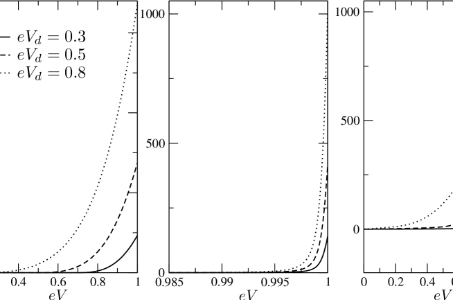
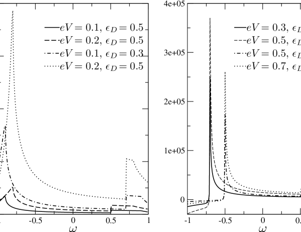
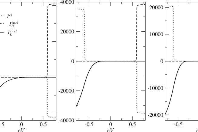
We calculate numerically the PAT currents in the three above cases: single and two quasiparticle tunneling, and Andreev reflection. All energies are measured with respect to the superconducting gap . In these units we chose and . Currents are typically plotted as a function of the DC bias voltage of the detector, for several values of the mesoscopic bias voltage (the “environment”). Our motivation is to consider the PAT currents with the condition (), where the effect of the environment on the PAT current is most pronounced, and we shall predict that two electrons tunneling as a Cooper pair (Andreev processes) contributes the most to the PAT current, except close to . Because of the symmetry between negative and positive , we display the results for . The PAT currents for the three above processes are plotted next to one other in Fig. 5 for comparison.
We find in Fig. 5 that if the chemical potential of the normal metal lead is close to the potential of the superconductor lead (), the PAT currents in the three cases are suppressed. For the two cases of quasiparticle tunneling, the PAT currents are equal to zero below a certain threshold. The single quasiparticle current differs from zero at a threshold which is identified as , that is quasiparticles are able to tunnel above that superconductor gap only if they can borrow the necessary energy from the mesoscopic device. This explains why the curves associated with different values of the mesoscopic device bias voltage are shifted to the right as decreases. For two quasiparticle particle tunneling, we observe that the PAT current has a similar threshold, which, compared to Fig. 5a, is pushed toward the right in Fig. 5b, because more energy is needed to transfer two electrons above the gap, compared to a single electron. Nor surprisingly, the curves corresponding are once again shifted to the right with decreasing . These curves all have a sharp maximum at .
We turn now to the Andreev PAT difference current, which dominates the two above processes at small and moderate bias. Note that the total Andreev current contains an elastic contribution as well as an inelastic contribution below the gap, contrary to quasiparticle tunneling which have contributions below the gap only because these processes are photo-assisted. Because we are computing the difference between PAT current with and without the mesoscopic bias voltage, we expect that the elastic contribution cancels out. However the first term of Eq. (37) tells us that the presence of the environment also gives rise to an effective elastic contribution to the PAT Andreev difference current. Unfortunately, this elastic correction is not small compared to the true Andreev current.
Looking at Fig. 5, we note that the PAT curve for Andreev processes is shifted to the left when the bias of the mesoscopic device is increased. The environment provides/absorbs energy to pairs of electrons whose energies are not symmetrical with respect to the superconducting chemical potential. At very weak , the elastic correction is small compared to the true Andreev current. We expect the PAT current contributions to originate from pairs of electrons in the normal metal below the superconducting chemical potential which can extract a photon from the environment. At the same time, Cooper pairs can be ejected in the normal metal as a reverse Andreev processes provided they borrow a photon to the environment. There is a balance between the right and left currents at very weak bias.
As the bias is increased, electrons pairs whose energies are above this chemical potential will now be able to yield a photon to the environment, giving rise to an increase of the inelastic PAT current. Also, the reverse Andreev process mentioned above becomes more restricted because the available empty states for electrons in the leads lie higher at positive bias. The elastic PAT current (not shown in the figures) increases when we increase the detector bias but it is always smaller than the inelastic contribution. The total PAT current increases gradually (Fig. 5, right panel).
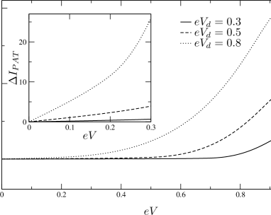
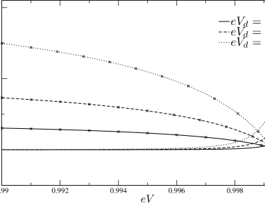
A zoom of this Andreev contribution is made in the region of small bias. There is in fact no threshold for the PAT Andreev current: for small bias, it has a linear behavior (Fig. 6). According to Eq. (37), when , the inelastic difference current of a Cooper pair tunneling from S to L by absorbing energy from mesoscopic device vanishes. The PAT current now describes two electron tunneling from L to S elastically or inelastically. In this intermediate bias regime, the elastic and inelastic contributions have now a tendency to cancel each other. The current reaches a maximum close to the gap, and then it decreases dramatically at the gap. This is consistent with the fact that for positive bias, the initial state for two quasiparticle tunnel processes and for Andreev reflection is precisely the same: close to the gap two quasiparticle tunneling takes over the Andreev process. It becomes more efficient for electrons to be activated above the gap than to be converted into a Cooper pair because the energy loss needed for the latter is quite large. Unlike a conventional normal metal – superconductor junction with elastic scattering only, where the relative importance of quasiparticle tunneling and Andreev reflection are interchanged precisely at the gap, here the dominance of quasiparticle tunneling manifests itself before the voltage bias reaches the gap. Note also in Fig. 5, that the magnitude of the Andreev current before the two quasiparticle threshold is precisely the same as the magnitude of the two quasiparticle at , which confirms this conversion scenario. A comparison of the two processes is displayed in Fig. 7.
In practice, the different contributions to the PAT current cannot be separated: one measures the sum of the three contributions which are plotted in Fig. 5. However, we claim that for a broad voltage range (from to the two quasiparticle threshold), the main contribution to the current comes from photo-assisted Andreev processes. The confrontation of Eq. (37) with an experimental measurement of the PAT current below the gap could thus serve an effective noise measurement, as the weight functions and are known.
Notice that in all our numerical results, the PAT currents are plotted in units of . We put some tentative numbers in these quantities. Here is the effective transmission coefficient of the NS interface, , is the transmission of the quantum point contact to be measured, ( is the resistance quantum) is the resistance which enters the transimpedance. This implies, e.g. for the PAT current in Fig. 6 at the top of the peak, with the device bias , which seems an acceptable value which is compatible with current measurement techniques.
III Tunneling current through a NDS junction
We now turn to a different setup for noise detection where electrons in a normal metal lead transit through a quantum dot in the Coulomb blockade regime before going into the superconductor. The essential ingredients are the same as the previous section, except that additional energy filtering occurs because of the dot. In this section, we choose the parameters of the device so that only Andreev processes are relevant.
III.1 Model Hamiltonian
The Hamiltonian which describes the decoupled normal metal lead – dot – superconductor – environment (mesoscopic circuit) system reads
| (43) |
where the Hamiltonian of normal metal lead and superconductor lead are described as above.
The Hamiltonian for the quantum dot reads
| (44) |
where will be assumed to be infinite, assuming a small capacitance of the dot. We consider that the dot possesses only a single energy level for simplicity.
The tunneling Hamiltonian includes electron tunneling between the superconductor and the dot, as well as the tunneling between the dot and the normal metal lead
| (45) | |||||
the indices k, D, q refer to the normal metal lead, quantum dot, superconductor. We consider the simple case , and .
For photo-assisted Andreev processes, one needs to carry out calculations of the matrix element in Eq. (10) to fourth order in the tunneling Hamiltonian. In what follows, we assume that the dot is initially empty, owing to the asymmetry between the two tunnel barriers. The barrier between the normal metal lead and the dot is supposed to be opaque compared to that between the dot and the superconductor. As a result, the rate of escape of electrons from the dot to the superconductor is substantially larger than the tunneling rate of electrons from the normal lead to the dot (see below for actual numbers).
There are two possibilities for charge transfer processes: a Cooper pair in the superconductor is transmitted to the normal lead or vice versa. The first process involves the electron from a Cooper pair tunneling onto the dot, next this electron escapes in the lead; the other electron from the same Cooper pair then undergoes the same two tunneling processes. Similar transitions, in the opposite direction, are necessary for two electrons from the normal lead to end up as a Cooper pair in the superconductor. Note that this description of events assumes implicity that superconductor lead remains in the ground state in the initial and final states (Andreev process). On the other hand, if normal metal lead is initially in the ground state (filled Fermi sea), it is left in an excited state with two electrons having energies above Fermi energy in the final state. The extra energy has been provided by the environment. Typically,
| (46) |
where denotes a ground state, which corresponds to a filled Fermi sea for the normal electrode. is the vacuum of the quantum dot, and denotes the initial state of the environment. On the other hand our guess for the final state should read
| (47) |
when a Cooper pair is emitted from S, or
| (48) |
when superconductor lead absorbs a Cooper pair. Here, is the final state of the environment. The justification for the choice of Eqs. (47) and (48) is the same as in Sec. II.5.
III.2 General formula for the photo-assisted Andreev current
For the case of two electrons tunneling from superconductor lead to normal metal lead, the current reads
| (49) | |||||
The problem is thus reduced to the calculation of correlators of the tunneling Hamiltonian in the ground state. Using Wick’s theorem, these can be expressed in terms of single particle Green’s function because the Hamiltonian of the isolated components is quadratic (except, maybe for the environment, which is dealt separately). We can now write the tunneling current as a function of the normal (and anomalous) Green’s functions of the normal metal lead, , the quantum dot, , and the superconductor, (which are shown in Appendix B)
| (50) | |||||
The result for the current contains both an elastic and an inelastic contribution. The elastic contribution reads
| (51) | |||||
with is the original denominator which is not affected by the environment, which is defined by Eq. (64), and is the denominator product affected by the environment (see Eq. (65) of Appendix D). The inelastic contribution reads
| (52) | |||||
where is the denominator product attributed to the inelastic current, which is defined in Eq. (66) of Appendix D.
Here, , define the tunneling rates between the superconductor and the dot, between the dot and the normal metal lead, respectively, with and the density of states per spin of the two metals in the normal state, at the chemical potentials and , respectively. All contributions to the current contain denominators where the infinitesimal (adiabatic switching parameter) is included in order to avoid divergences. In fact, it has been shown in Refs. recher_sukhorukov_loss, ; lehur, that a proper resummation of the perturbation series, including all round trips from the dot to the normal leads, leads to a broadening of the dot level. We take into account this broadening by replacing by with into our calculations (including only a broadening due to the superconductor). As mentioned above, we have assumed that . In order to avoid the excitation of quasiparticles above the gap, these rates need also to fulfill the condition . In what follows, we keep the notation in our expressions, bearing in mind that it represents the line width associated with the leads. For numerical purposes, it will be sufficient to assume that is kept very small compared to the superconducting gap, as well as all the relevant level energies (dot level position, bias voltages, etc…).
The above expressions constitute the second main result of this work: one understands now how the current fluctuations in the neighboring mesoscopic circuit give rise to inelastic and elastic contributions in the current in the NDS device.
We find that both right and left current contributions have the same form. The current - current fluctuations of the mesoscopic device affect the detector current at the energy corresponding to the total energy of two electrons exiting in (or entering from) the normal lead. Therefore, we proceed to the same change of variables a for the single NS junction.
For , elastic current contributions in are present but the same contributions in vanish (the opposite is true for the case of ).
Changing variables in the inelastic contributions, and defining the kernel functions , as in Appendix D, for and , we obtain:
| (53) | |||||
with .
The first term in Eq. (53) describes the elastic contribution in the PAT current. Although we are less interested in this contribution, we cannot ignore it in practice because it contributes to the total . The environment affects this current contribution but at the end of the tunneling processes, there is no energy exchanged between the device and the detector circuit. The second term in Eq. (53) describes the tunneling of a Cooper pair from the normal lead to the superconductor via the quantum dot, with energy exchange. The electrons can absorb energy (in the case their total energy is smaller than the superconductor chemical potential ) or emit energy (if their total energy is bigger than ). The last term in Eq. (53) describes the inverse tunneling process: a Cooper pair absorb energy from the neighboring device, its constituent electrons then tunnel to the normal lead. In this event, the total energy of the outgoing electrons is positive. If on the contrary, this total energy is negative, the Cooper pair has emitted energy to the device.
In order to understand how the detector circuit affects the behavior of the current (in the presence of the environment), we investigate the weight functions and separately.
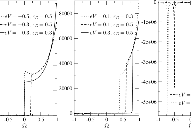
The weight function is plotted in Fig. 8 as a function of frequency , for two values of the bias voltage and two values of the dot level position. This elastic kernel is symmetric under bias voltage reversal (). From the right panel of this figure, where we consider , we find that there is a small step at and a sharp peak at . The peak is assymetric, and its height is much larger than that of the step. When , changes sign and becomes negative. The voltage bias mainly affects the amplitude of the peak and of the step in . The left panel of Fig. 8 describes when . The peak height decreases quite fast as a function of , and its location is shifted at . The peak is symmetric for large bias.
We turn now to the truly photo-assisted processes, which involve either absorption or emission of energy. The kernel is plotted in Fig. 9 as a function of frequency , which corresponds to the total energy of two electrons, for . In the left panel, is negative, and in the center panel, is positive but , and finally the right panel of Fig. 9 describes . We find that when , there is a step at . When we increase close to , the step still dominates but there is a small peak at . When this (inverted) peak is very sharp. This is explicit in the right panel. The inverted peak, which has a large amplitude, makes it now difficult to observe the step. The (inverted) peak is located at . Again, mostly affects the amplitude of . For (not shown), the result is similar to that of with opposite , but the amplitude of the peak is doubled compared to that of when .
Note that understanding the behavior of the two weight functions as a function of the different parameters ( and ) of the detector is crucial. It allows to control the effect of the device voltage bias on the DC current of the detector, and it is therefore the key for extracting the noise from the measurement of this DC current.
III.3 Application to a Quantum Point Contact
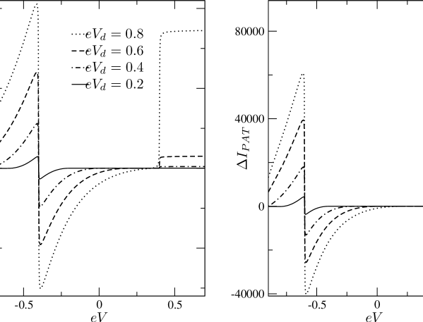
We now calculate from Eq. (53) with the spectral density of excess noise of a Quantum Point Contact, given by Eq. (41). We consider the PAT current as a function of the detector voltage for several values of the device voltage , which are shown in Fig. 10. We find that there are two values of at which changes drastically. First, there is a step located at and second, a Fano-like peak appears at . The (negative) derivative at seems to diverge. The high of both the peak and the step increase in a monotonous manner as a function of the ratio of the device voltage divided by the dot level . When is small, the peak is much higher than the step. Increasing , the peak further increases, but the step height increases faster, starting from the threshold device voltage . In Fig. 10, we find that for and , the peak height is still higher than the step, but with , and , the step becomes higher than the peak. Here for specificity, we only consider the case where , but results for can be obtained in a similar manner, exploiting electron hole symmetry.
In order to further understand the behavior of , we consider the different contributions of this photo-assisted current, which are shown in Fig. 11. Specifically, we plot the elastic current renormalized by the environment, as well as the right and left inelastic currents. We find that the elastic part is symmetric between positive and negative. It is almost equal to zero when . It shows a step at . This can be understood from the fact that at the threshold electrons tunnel from the normal metal lead to the superconductor predominantly by making resonant transitions through the dot. Electrons easily tunnel to the quantum dot, in a sequential manner becoming a Cooper pair in the superconductor. For , the same reasoning can be made for incoming holes, or equivalently for electrons exiting the superconductor: a Cooper pair in the superconductor is split into two electrons, which tunnel to the quantum dot and then to the normal metal lead. Because of the energy conservation condition, it is then necessary to have .
Turning now to the inelastic current, we consider the contribution of 2 electrons being transfered inelastically from the normal metal lead to the superconductor, which is called the in Fig. 11. When , electrons tunnel through the quantum dot to the superconductor by absorbing or emitting energy to environment. However, as in the elastic case, the transfer from the normal metal to the dot is more favorable when , which explains the presence of the step in at this bias voltage.
Next, we consider the contribution of two electrons tunneling from the superconductor to the normal metal lead, which is called in Fig. 11. When is positive, is nonzero only when , this case corresponds to the process of the Cooper pair absorbing energy from environment to tunnel to the normal metal lead. If , a small step occurs (not shown) at corresponding to the activation of the two Cooper pair electrons on the dot: this small feature can only be seen by zooming in the picture. When is negative, the absorption of energy from the environment becomes much more favorable. Because of this, the analog of the step corresponding to in the elastic current is smoothed out, and it saturates around . Nevertheless, also contains contributions where electrons emit energy to the environment. Starting from , the process of the Cooper pair tunneling to the normal metal lead and emitting energy to environment has first a small contribution to but it really becomes noticeable below and eventually saturates for lower bias voltage (not shown). As the voltage of the mesoscopic device is lowered (left to right panels of Fig. 11), two things occur: first, the amplitude of all current contributions decreases, second, the smoothing of the is reduced because the range of energy available to absorption and emission is reduced.
In brief the sum of the contributions for emission and absorption in have a tendency to compensate the elastic current at voltages where saturation is reached. ¿From the above considerations, we therefore can interpret the curve of , and we understand when the detector circuit absorbs or emits energy from/to mesoscopic device: when is negative, the PAT current is mainly due to absorption for , and emission for .
Note that in all our numerical results, the PAT current is in units of . To check the observability of these predictions we estimate: , , , , (see also Ref. aguado_kouwenhoven, ; deblock1, ; deblock2, ; recher_lossPRL, ). This implies, e.g. for the PAT current in Fig. 10 when the detector bias is close to , with the device bias . This value is acceptable if one compares it with the value of current which has been estimated in Ref. aguado_kouwenhoven, . It is also acceptable with present day detection techniques.
IV Conclusion
In conclusion, we have presented a new capacitive coupling scheme to study the high frequency spectral density of noise of a mesoscopic device. As in the initial proposal of Ref. aguado_kouwenhoven, , the effect of the noise originating from a mesoscopic device triggers an inelastic DC current in the detector circuit. This inelastic contribution can be thought as a dynamical Coulomb blockade effect where the phase fluctuations at a specific junction in the detector circuit junction are related to voltage fluctuations in same junction. In turn, such voltage fluctuations originate from the current fluctuations in the nearby mesoscopic device, and both are related by a trans-impedance. The novelty is that here, because the junction contains a superconducting element, in the subgap regime, two electrons need to be transferred as the elementary charge tunneling process. In a conventional elastic tunneling situation, the two electrons injected from (ejected in) the normal metal lead need to have exactly opposite energies in order to combine as a Cooper pair in the superconductor. Here, this energy conservation can be violated in a controlled manner because a photon originating from the mesoscopic circuit can be provided to/from the constituent electrons of the Cooper pair in the tunneling process.
We have computed the DC current in the detector circuit for two different situations. In a first step, we considered a single NS junction, and we computed all lowest order inelastic charge transfer processes which can be involved in the measurement of noise: the photo-assisted transfer of single (and pairs of) electrons (with energies within the gap) into quasiparticle(s) above the gap, and photo-assisted Andreev transfer of electrons as a Cooper pair in the subgap regime. It was shown that the latter process dominates when the source drain bias is kept well within the gap. Close but below the gap, the absorption of quasiparticle dominates, and we observe a crossover in the current between the Andreev and quasiparticle contributions. For the above processes, we demonstrated the dependence of the DC current on the voltage bias of the mesoscopic device, chosen here to be a quantum point contact. When this bias is increased, the overall amplitude of the spectral density and its width scale as , so that the phase space (the energy range) of electrons which can contribute to the Andreev processes is magnified. We therefore have gained an understanding about how the measurement of the DC current can provide useful information on the noise of the mesoscopic device. Nevertheless, one should point out that with this NS setup, it is difficult to isolate the contribution of the photo-assisted current which involves, respectively, the absorption and the emission of photons from the mesoscopic device. For biases close to the chemical potential of the superconductor, both will typically contribute to the photo-assisted current.
Next, we considered a more complex detector circuit where the normal metal and the superconductor are separated by a quantum dot which can only accommodate a single electron at a given time. There, the dot acts as an additional energy filtering device, with the aim of achieving a selection between photon emission and absorption processes. We decided to restrict ourselves to the photo-assisted Andreev (subgap) regime, assuming that the dot level is well within the gap. By computing the total excess photo-assisted current as well as its different contributions for absorption and emission, and right and left currents, we found that for DC bias voltages comparable to it is possible to make such a distinction. The NDS detection setup could therefore provide more information on the spectral density of noise than the NS setup, but its diagnosis would involve the measurement of smaller currents than the NS setup, because of the presence of two tunnel barriers instead of one.
Note that normal lead – quantum dot – superconductor setups have already been investigated theoreticallykondo_effect and experimentally recently graeber . In such works, the emphasis was to study how the physics of Andreev reflection affected the Kondo anomaly in the current voltage characteristics. In Ref. graeber, , the quantum dot consisted of a carbon nanotube making the junction between a normal metal lead and a superconductor. Here, we did not consider the quantum dot in the Kondo regime, and we included interactions on the dot in the Coulomb blockade regime.
A central point of this study is the fact that all contributions to the photo-assisted current, for both the NS and NDS setups, can be cast in the same form:
| (54) |
Where is a Kernel which depends on the nature (elastic or inelastic) as well as the mechanism (single quasi-particle or pair tunneling) of the charge transfer process. When dealing with an elastic process, one understand that the environment renormalizes the DC current even when no photon are exchanged between the two circuits. In the case of inelastic tunneling only, the frequency corresponds to the total energy of the two electrons which enter (exit) the superconductor from (to) the normal metal lead. Finally, the sign of the frequency (and thus the bound of the integral in Eq. (54), which are left “blank” here) decides whether a given contribution corresponds to the absorption or to the emission of a photon from the mesoscopic circuit.
The present proposal has been tested using a quantum point contact as a noise source, because the spectral density of excess noise is well characterized and because it has a simple form. It would be useful to test the present model to situations where the noise spectrum exhibits cusps or singularities. Cusps are known to occur in the high frequency (close to the gap) noise of normal superconducting junctions. Singularities in the noise are know to occur in chiral Luttinger liquid, tested in the context of the fractional quantum Hall effectfrequency_fqhe . Such singularities or cusps should be easy to recognize in our proposed measurement of the photo-assisted current.
On general grounds, we have proposed a new mechanism which couples a normal metal – superconductor circuit to a mesoscopic device with the goal to understand the noise of the latter. The present setup suggest that it is plausible to extract information about high frequency noise. High frequency noise detection now constitutes an important subfield of nano/mesoscopic physics. New measurement setup schemes which can be placed “on-chip” next to the circuit to be measured are useful for further understanding of high frequency current moments.
Acknowledgements.
We thank Richard Deblock for valuable discussions.V Appendix A
In this Appendix, we define , , and in the
| (55) | |||||
| (56) | |||||
| (57) | |||||
VI Appendix B
In this Appendix, we recall the definition of Keldysh Green’s functionsmahan . First, we define the anomalous Green’s function, describing the pairing of electrons with opposite spin in the superconductor:
If both and are in the upper branch, and or both and are in the lower branch, and then . These Green’s functions enter the description of the Andreev process.
If we consider the single quasiparticle tunneling in the superconductor, we use the conventional definition of the Green’s function as for normal metals.
Secondly, we define the Green’s function of the one level QD: .
Simplifications occur because the quantum dot has a singly occupied level with energy , the first electron is transferred to the lead before the second hops on the quantum dot so that in our work, we only consider the QD Green’s function where both time quantities and are in the upper or lower branch, and the Green’s function values only when if , in the upper branch and if , in the lower branch, then .
The Green’s function in the normal metal lead reads: .
In our work, we consider the cases where two electrons tunneling from/to normal metal lead, so that we only consider normal metal Green’s function where and are in the different branches. For the case electrons tunneling from the superconductor to the normal metal, we use the greater Green’s function with . For the case electrons tunneling from the normal metal to the superconductor, we use the lesser Green’s function with .
VII Appendix C
In this part, we present the denominator products which appear in the tunneling current through the NS junction as a Cooper pair. Such denominators come from the energy denominators of the transition operator T.
| (58) |
| (59) | |||||
| (60) | |||||
Change variables in , as
We define
| (61) | |||||
then we define the weight functions as
| (62) | |||||
| (63) | |||||
VIII Appendix D
In this Appendix, we present the denominator products which appear in the tunneling current through the NDS junction.
is the original denominator which is not affected by the environment
| (64) | |||||
and is the denominator product affected by the environment
| (65) | |||||
where is the denominator product attributed to the inelastic current (affected by environment) and it is defined as
| (66) | |||||
We define
| (67) |
If then
else
Then we define
| (68) | |||||
| (69) | |||||
| (70) | |||||
Since , , so , . But in fact, if we change the name of variable then change variable , we will obtain the same formula for both cases and . Since are independently equivalent, so that it is evidently . Hereafter, we neglect the or index in these functions.
If , the elastic current contributions in exist but the elastic current contributions in vanish (in contrast to the case of ).
We change variables in inelastic contributions as
and define
| (71) |
| (72) | |||||
with .
References
- (1) S.R. Eric Yang, Solid State Commun. 81, 375 (1992).
- (2) Y.M. Blanter and M. Büttiker, Phys. Rep. 336, 1 (2000).
- (3) C. Chamon, D. E. Freed, and X. G. Wen, Phys. Rev. B 53, 4033 (1996).
- (4) T. Martin and R. Landauer, Phys. Rev. B 45, 1742 (1992); M. Büttiker, Phys. Rev. B 45, 3807 (1992).
- (5) G. B. Lesovik and R. Loosen, Pis’ma Zh. Éksp. Teor. Fiz. 65, 280 (1997) [JETP Lett. 65, 295, (1997)].
- (6) N. M. Chtchelkatchev, G. Blatter, G. B. Lesovik and T. Martin, Phys. Rev. B 66, 161320(R) (2002).
- (7) A. V. Lebedev, G. B. Lesovik, and G. Blatter, Phys. Rev. B 72, 245314 (2005).
- (8) A. V. Lebedev, A. Crepieux, and T. Martin Phys. Rev. B 71, 075416 (2005).
- (9) B. Trauzettel, I. Safi, F. Dolcini, and H. Grabert, Phys. Rev. Lett. 92, 226405, (2004).
- (10) R. Aguado and L. Kouwenhoven, Phys. Rev. Lett. 84, 1986 (2000).
- (11) R. Deblock, E. Onac, L. Gurevich, and L. P. Kouwenhoven, Science 301, 203 (2003).
- (12) P.-M. Billangeon, F.Pierre, H. Bouchiat, and R. Deblock, Phys. Rev. Lett. 96, 136804 (2006).
- (13) A. Onac, F. Balestro, B. Trauzettel, C. F.J. Lodewijk, and L. Kouwenhoven, Phys. Rev. Lett. 96, 026803 (2006).
- (14) G. L. Ingold and Yu. V. Nazarov, in Single Charge Tunneling, H. Grabert and M.H. Devoret eds. (Plenum, New York 1992).
- (15) G. E. Blonder, M. Tinkham, and T. M. Klapwijk, Phys. Rev. B 25, 4515 (1982).
- (16) U. Gavish, Y. Levinson, and Y. Imry, Phys. Rev. B. 62, 637 (2000).
- (17) T. Martin in Les Houches Summer School session LXXXI, edited by E. Akkermans, H. Bouchiat, S. Gueron, and G. Montambaux (Elsevier, 2005).
- (18) G. Falci, R. Fazio, A. Tagliacozzo, and G. Giaquinta, Europhys. Lett. 30, 169 (1995).
- (19) P. Devillard, R. Guyon, T. Martin, I. Safi, and B. K. Chakraverty, Phys. Rev. B 66, 165413 (2002).
- (20) In explicit calculations we set but restore in the fundamental quantities and in the numerical estimate of the PAT current.
- (21) P. Recher, E.V. Sukhorukov, and D. Loss, Phys. Rev. B 63, 165314 (2001).
- (22) G. B. Lesovik, T. Martin, and G. Blatter, Eur. Phys. J. B 24, 287 (2001).
- (23) P. Recher and D. Loss, Phys. Rev. Lett. 91, 267003 (2003).
- (24) I. Safi, P. Devillard and T. Martin, Phys. Rev. Lett. 86, 4628 (2001).
- (25) G. B. Lesovik, JETP Lett. 49, 594 (1989).
- (26) E. Dupont and K. Le Hur, Phys. Rev. B 73, 045325 (2006).
- (27) J. B. Ketterson and S. N. Song, Superconductivity (Cambridge University Press, 1999).
- (28) R. Fazio and R. Raimondi, Phys. Rev. Lett. 80, 2913 (1998); Q. Sun, H. Guo and T. Lin, Phys. Rev. Lett. 87, 176601 (2001); A. Clerk, V. Ambegaokar and S. Hershfield Phys. Rev. B 61, 3555 (2000); JC Cuevas, A. Levy Yeyati and A. Martín-Rodero, Phys. Rev. B 63, 094515, (2001).
- (29) M.R. Gräber, T. Nussbaumer, W. Belzig, T. Kontos, and C. Schönenberger, in Quantum Information and Decoherence in Nanosystems, Proc. Rencontres de Moriond 2004; M.R. Gräber, T. Nussbaumer, W. Belzig, and C. Schönenberger, Nanotechnology 15, 479 (2004).
- (30) C. de C. Chamon, D. E. Freed, and X. G. Wen, Phys. Rev. B 53, 4033 (1996).