Magnetic properties and domain structure of
(Ga,Mn)As films with perpendicular anisotropy
Abstract
The ferromagnetism of a thin Ga1-xMnxAs layer with a perpendicular easy anisotropy axis is investigated by means of several techniques, that yield a consistent set of data on the magnetic properties and the domain structure of this diluted ferromagnetic semiconductor. The magnetic layer was grown under tensile strain on a relaxed Ga1-yInyAs buffer layer using a procedure that limits the density of threading dislocations. Magnetometry, magneto-transport and polar magneto-optical Kerr effect (PMOKE) measurements reveal the high quality of this layer, in particular through its high Curie temperature (130 K) and well-defined magnetic anisotropy. We show that magnetization reversal is initiated from a limited number of nucleation centers and develops by easy domain wall propagation. Furthermore, MOKE microscopy allowed us to characterize in detail the magnetic domain structure. In particular we show that domain shape and wall motion are very sensitive to some defects, which prevents a periodic arrangement of the domains. We ascribed these defects to threading dislocations emerging in the magnetic layer, inherent to the growth mode on a relaxed buffer.
pacs:
75.50.Pp, 75.30.Gw, 76.60.Es, 75.70.-iI Introduction
In the increasingly active field of research on spintronics, impressive progress has been made in the understanding and improvement of diluted magnetic semiconductors (DMS), in particular of (Ga,Mn)As.Matsukura et al. (2002) It is now well established that ferromagnetism in this material stems from the exchange interaction between the spins localized on the 3d shell of the magnetic ions and the itinerant carriers.Dietl et al. (2001a) Such an interplay between spin-polarized holes and the randomly distributed magnetic moments offers a novel set of phenomena not found in usual ferromagnets, such as the strong dependence of the Curie temperature on the carrier density (), and the electrical Ohno et al. (2000) and optical Koshihara et al. (1997) control of the ferromagnetism. Another remarkable feature is the huge sensitivity of the magnetic anisotropy on epitaxial strains, a behavior related to the valence band anisotropy.Dietl et al. (2001b) Usually, compressive strains favor an in-plane easy magnetization, as in the case of a (GaMn)As layer grown on a GaAs substrate, although this trend may be reversed at low carrier density.Sawicki et al. (2004); Thevenard et al. (2005) In counterpart, under tensile strains, when (GaMn)As is grown on a (InGa)As buffer layer,Shen et al. (1997) the magnetization becomes spontaneously oriented along the normal film to the film. Since only little information is available so far on (GaMn)As films with perpendicular magnetic anisotropy, we will focus here on their magnetization reversal and domain study. Moreover, as already reported for (GaMn)As with in-plane magnetic anisotropy,Edmonds et al. (2002) we show that the Curie temperature can also be significantly enhanced after a convenient annealing procedure of the sample that induces a higher metallic character to the layer and more uniform properties, such as wider magnetic domains.
Compared to the well-known magnetic behavior of 3d-metallic films, there are still open questions on the incidence of the specific nature of the exchange interaction in (GaMn)As, especially on the dynamics of the magnetization reversal and related phenomena, such as nucleation and domain wall motion. For in-plane magnetized (Ga,Mn)As layers, large (micrometers-wide) and homogenous magnetic domains have been observed by Welp et al. (2003) In that particular case, magnetization reversal occurs by rare nucleations and expansion of large and type of domains.
Up to now, only Scanning Hall Probe Microscopy has been used to investigate the magnetic domain structure in (GaMn)As with perpendicular anisotropy,Shono et al. (2000); Pross et al. (2004) but the area under study was limited to a range of a few tens of square micrometers, and information on the magnetic state was, in our opinion, too limited to extract quantitative parameters. Nevertheless, a typical domain width of a few micrometers has been estimated,Shono et al. (2000) consistently with theoretical arguments assuming regular stripe-domains in such a magnetic film.Dietl et al. (2001a)
In this paper we report on the preparation, the characterization and the magnetic properties of a thin (Ga,Mn)As layer grown in tensile strain on an (In,Ga)As buffer. A thorough characterization performed by combined X-ray diffraction, transmission electron microscopy, magnetization, magneto-optics, conductivity and magneto-transport measurements, confirmed the high structural and magnetic quality of the sample, that is significantly improved upon annealing.
Anomalous Hall effect and polar magneto-optical Kerr effect (PMOKE) are suitable for accurate measurements of the magnetization in thin ferromagnetic films with perpendicular anisotropy. Both observables are related to the out-of-plane component of the static magnetization M⊥ through static (Hall effect) or high frequency (PMOKE) conductivity non-diagonal tensor elements. Also note that no diamagnetic contribution needs to be deduced from Hall or PMOKE data since both effects are insensitive to a possible spurious magnetism of the substrate. In this article, PMOKE is used as the generic name. In fact, to be less sensitive to the field-induced Faraday rotation in glass windows of the cryostat, we measured the Polar Differential Circular Reflectivity using left or right-handed circularly polarized light. This effect is analogous, in reflection, to magnetic circular dichroism in light transmission. Note that PMOKE is much more sensitive to out-of-plane magnetization than longitudinal MOKE for an in-plane magnetized sample.Hrabovsky et al. (2002); Moore et al. (2003) PMOKE is sensitive to the valence and conduction band splitting,Lang et al. (2005); Beschoten et al. (1999) i.e. it varies like M⊥, as soon as measurements are carried far away from intense absorption bands, which is justified here using green light wavelength ( nm). Moreover, we checked that interference effects also have a negligible impact on measurements. Using PMOKE, dynamics of the field-induced magnetization reversal have been investigated here down to the millisecond range. The magnetic relaxation has been further analyzed by considering nucleation and domain expansion by wall propagation. Our conclusions were confirmed from the direct imaging of the magnetic domain structure by PMOKE microscopy. Thus, micrometer-wide domains, pinned by defects, were evidenced both in the remnant and in-field states.
II Sample growth and structural characterization
The sample was prepared by molecular beam epitaxy. It is formed by a 50 nm thick Ga1-xMnxAs layer grown on an Ga1-yInyAs relaxed buffer layer, itself deposited on a semi-insulating (001) GaAs substrate. Special care was taken to minimize the number of threading dislocations emerging in the magnetic layer, following the technique developed by Harmand et al. (1989) The Ga1-yInyAs buffer consists first of a 0.5 m thick layer grown by increasing monotonously the In content from y = 0 to 9.8 %. Then 2-3 m of Ga0.902In0.098As were grown above before depositing the Ga1-xMnxAs layer. The graded Ga1-yInyAs layer prevented the formation of a too large amount of misfit dislocations, sources of threading dislocations propagating along towards the surface, as usually observed in abrupt mismatched interfaces. Here, dislocations were distributed along the graded layer, which limits the nucleation of threading dislocations.Harmand et al. (1989) Indeed, a very low density of emerging dislocations, cm-2, was measured using an anisotropic revealing etchant. Moreover, the substrate temperature was set to 400∘C during the growth of the buffer to avoid the formation of three-dimensional strain-induced islands, a process favored at higher temperature.Harmand et al. (1989) The Ga1-xMnxAs layer was deposited at 250∘C. The surface is crossed-hatched, due to surface roughness originating from bunches of misfit dislocations propagating along and inside the graded layer. and X-ray diffraction space mappings showed that the (In,Ga)As layer was almost completely relaxed (at 80%), insuring that the Ga1-xMnxAs layer was still under tensile strain. The Mn concentration x0.07 was determined by comparison with Ga1-xMnxAs layers grown in the same conditions, directly on GaAs (001). Finally, a part of the sample was annealed under nitrogen atmosphere for 1 hour in a tube furnace at 250∘C to out-diffuse the interstitial Mn atoms, in order to improve magnetic properties.Edmonds et al. (2002) For magneto-transport measurements, the layer was processed into Hall bars by UV-lithography and wet chemical etching. Ti/Au contacts were used.

III Magnetic, magneto-transport and magneto-optic measurements
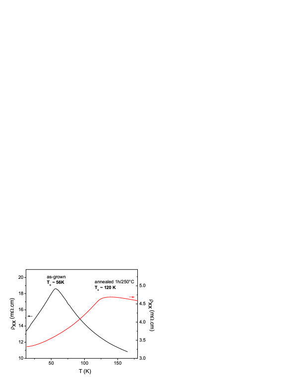
As quoted above, it is well known that the annealing process improves both the transport and magnetic properties of (GaMn)As deposited on (001) GaAs.Edmonds et al. (2002) This is also true for a tensile-strained (GaMn)As film grown on (In,Ga)As, as checked by resistivity (Fig. 1), and Hall hysteresis loop (Fig. 2) extracted from the transverse resistivity, as described later in the text. The resistivity of the as-grown Ga0.93Mn0.07As film on (In,Ga)As is rather high ( mW.cm at 4K), showing a maximum at Tc = 56 K (Fig. 1). In counterpart, the annealed film exhibits a much lower resistivity, i.e. a more metallic character ( = 2.58 mW.cm at 4K) at low temperature, and a remarkably higher Curie temperature, K. As often found for as-grown samples with in-plane magnetic anisotropy, the Hall hysteresis loops of the non-annealed sample exhibit a complex shape at low temperature Lang et al. (2005). In the present case, and coherently with previous results,Sawicki et al. (2004); Liu et al. (2005) the evolution of the loop shape between 22 K to 4 K (Fig. 2a) suggests an out-of-plane to in-plane spin reorientation transition when decreasing the temperature. In counterpart, the hysteresis loops of the annealed Ga0.93Mn0.07As film (Fig. 2b) are perfectly square at all temperatures below Tc, consistently with a marked out-of-plane magnetic anisotropy. The magnetization of the annealed sample, measured by a Superconducting Quantum Interference Device (SQUID) also shows a behavior very consistent with Hall measurements, namely a square hysteresis loop at 4 K (Fig. 3), with a coercive field of 40 5 Oe, obtained with a low field sweeping rate (0.08 Oe/s). In the following, we will only focus on properties of the annealed film.

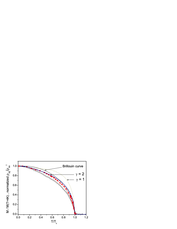
The temperature dependence of the magnetization measured by SQUID in a small magnetic field (250 Oe) applied along the growth axis is presented in Fig. 4. It shows a smooth decline with increasing temperature and magnetization once again cancels at K. For comparison we have plotted the mean-field Brillouin function expected for an ideal ferromagnet. Only a small departure from the Brillouin curve is observed. Such a behavior is predicted in GaMnAs layers,Dietl et al. (2001b) and may arise partly from the fact that the spin-splitting of the valence band is comparable to the Fermi energy, as explained within the mean-field theory frame. We note that the discrepancy between these two curves remains fairly low, reaching 20 % at most, giving another indication of the high quality of this sample. SQUID and PMOKE measurements also prove that the annealed (GaMn)As film is not ferromagnetic at room temperature. More precisely, as compared to results for MnAs clusters,Primus et al. (2005) high field (6.5 kOe) PMOKE data exclude that more than 0.5 % of Mn ions enter in the formation of ferromagnetic MnAs nanoclusters.
We now return to the Hall measurements. In GaMnAs layers, the anomalous Hall resistivity, , has been found to be proportional to , so that , Ra being called the anomalous Hall term. It directly probes the carrier-mediated ferromagnetism, since it is induced, through the spin-orbit coupling, by anisotropic scattering of spin-up and spin-down carriers. Ra was shown to be proportional to , where is the sheet resistivity (Fig. 1). The value of is still a matter of debate (for a review, see Sinova et al. (2004)). It was first proposed to depend on the spin scattering mechanism, with = 1 in the case of ”skew scattering”, or = 2 for ”side-jump scattering”.Berger and Bergmann (1979) More recently, Jungwirth et al. (2002) showed that the dominant contribution to Ra would be due to a scattering-independent topological contribution, which also gives = 2.
Therefore, the anomalous Hall resistivity, gives access to perpendicular hysteresis loops, yielding information for example on the coercivity (as seen in Fig. 2 where the ratio was plotted using = 2), the remnant magnetization, and the thermal dependence of the saturated magnetization.
The thermal dependence of the remnant Hall effect is also presented in Fig. 4 as a function of , considering = 1 or = 2. The choice of has a rather large impact on the result below . For = 1, the Hall effect is nearly constant from K up to 0.6 , but shows a rapid drop at Tc, whereas for = 2, it decreases more progressively at high temperature. Both curves are always located above the magnetization curve up to Tc. While the thermal dependence of the = 2 curve is similar to that of the magnetization within 10% at most, the = 1 curve exceeds magnetization values by up to 36%. Furthermore the = 2 curve closely follows the Brillouin curve. Lastly, the = 2 curve matches entirely the remnant PMOKE signal (Fig. 4), which is another measure of the magnetization. Note that the anomalous Hall term Ra may not remain perfectly constant within the whole temperature range. Nevertheless, we obtained a very consistent set of results when comparing the ratio / with = 2 to the magnetization and PMOKE data.
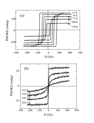
As in Hall magnetometry, we measured very square PMOKE magnetic hysteresis loops over the full range of temperatures up to Tc = 130 K (Fig. 5a). This proves that domain reversal occurs very abruptly and uniformly over the sample, as soon as one reaches the coercive field. The quality of the Ga0.93Mn0.07As annealed film is also confirmed by the abrupt disappearance of the remnant magnetization at (Fig. 5b). At low temperature, loops do not saturate in field as abruptly in PMOKE (Fig. 5a) as in Hall magnetometry (Fig. 2). This is certainly due to the fact that the probed region is larger in PMOKE (1 mm2) than in Hall magnetometry (10-2 mm2). As we shall see in PMOKE microscopy, the occurrence of hysteresis loop tails is due to a few hard defects that pin small reversed magnetized filamentary domains even in fields larger than the coercive field. At finite temperature, the coercive field deduced from PMOKE measurements is always expected to be larger than in Hall magnetometry and magnetization measurements because of the much faster field sweeping rate in the former case Moore et al. (2003); Ferre (2001) (200 Oe/s).
IV Magnetization reversal dynamics and domains
As mentioned above, dynamics of the magnetization reversal manifests itself by an increase of the coercive field with the field sweeping rate. A clearer view of the magnetization reversal dynamic behavior is given from magnetic relaxation curves, also called magnetic after-effect. The film is first magnetically saturated in a positive field of 135 Oe, and suddenly inverted, at t = 0, to a negative value , that is smaller than the measured coercive field. The magnetization of the film being in a metastable state, it tends to reverse gradually with time towards the negative saturated magnetization value. Obviously, the relaxation of the magnetization becomes faster when increasing . Previous results have been reported on (GaMn)As films with in-plane anisotropy.Moore et al. (2003)
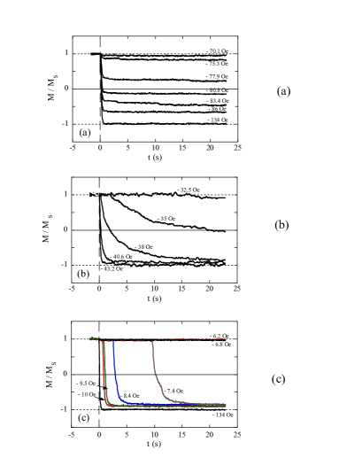
Results on the magnetic after-effect for the annealed (GaMn)As film, measured by PMOKE at 1.8 K, 77K, and 100 K, i.e. below K, are depicted on Fig. 6 a,b,c. The time dependent variation of the PMOKE signal is measured on a film area delimited by the light spot size (about 1 mm2). As we shall see later, the magnetization reversal is initiated by rare nucleation events, and develops by subsequent domain wall propagation. At very low temperature, the thermal activation is not very efficient, so that the applied field H must overcome the height of local energy barriers for wall propagation. In other words, if H is higher than the nucleation field and most of the distributed pinning barriers, the wall will propagate rapidly until reaching centers with high energy barriers. After that, walls will only move by poorly efficient thermal activation. This behavior is well revealed on relaxation curves at T = 1.8 K (Fig. 6a). At temperatures closer to Tc, most of the propagation energy barriers become weaker than the energy barrier for nucleation. Thus, a thermally activated lag time is required for nucleation; it is followed by rapid domain wall propagation. This gives rise to typical magnetization relaxation curves presented on Fig. 6c, at 113.5 K, when nucleation occurs outside of the investigated light spot area. As expected, the probability of nucleation, which follows a thermally activated Arrhenius law,Ferre (2001) increases rapidly with the applied field. In the intermediate temperature range ( K), one generally observes a rather monotonous decrease of the magnetization (Fig. 6b) when the light spot only checks a homogeneous sample area. As we shall see later, the investigated region can contain several strong pinning centers. In that case, the domain wall propagation is suddenly slowed down by local pinning, and then accelerated through a depinning process involving the relaxation of the bending energy. Similar dynamic behavior has been already evidenced in a pure metallic Au/Co/Au ultrathin film structure.Ferre (2001)
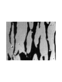
Finally, the domain structure and dynamics have been investigated by PMOKE microscopy. A similar set-up, working at room temperature, has been previously described.Hubert and Schäfer (1998); Ferre (2001) Since the long distance objective was located outside the cryostat vessel, the optical resolution was limited here to about 1.5 m at the used red optical wavelength ( = 650 nm). It is well known that the equilibrium demagnetized state of a perfect film with perpendicular anisotropy must be a stripe domain structure from which microscopic parameters may be deduced.Hubert and Schäfer (1998) However, as soon as extrinsic defects are efficient enough to pin the walls, the demagnetized state becomes highly perturbed and tends to decorate the assembly of pinning centers. As depicted on Fig. 7, this is the case of our Ga0.93Mn0.07As annealed film, where large up and down-magnetized (typically 15 m wide) domains are stabilized in the demagnetized state without reminiscence of any periodic ribbon domain structure that is expected in a defect-free sample.
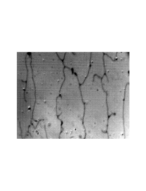
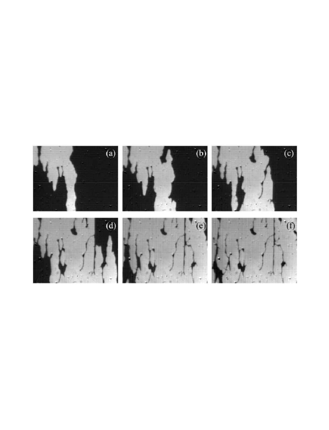
To get a better understanding of the magnetization reversal process, snapshots of successive magnetic states of an annealed Ga0.93Mn0.07As film, have been recorded at 77 K, using a magnetic after-effect procedure (Fig. 8). After saturating the magnetization in a positive field, a weak enough field (- 20.5 Oe) was applied to produce a slow magnetization reversal. An order of magnitude of the domain wall velocity is 10 m/s in a field of Oe. After nucleation of a down-magnetized nucleation center, located above the image frame, a down-magnetized (white) domain invades progressively the visualized area at the expense of the up-magnetized state (black) (Fig. 8a to d). So, nucleation is a rare event, and the magnetization reversal occurs by a rather uniform wall propagation. The front of propagation is irregular since walls are often pinned by defects that slow down their motion. After skirting a defect, the domain continues to grow by leaving a stable up-magnetized filamentary domain, also called unwinding 360∘ wall, along the direction of motion. Lemerle et al. (1997) During this process, random magnetization jumps, due to successive local depinnings, can take place after long lag times (Fig.8d to f); the resulting magnetization reversal slows down progressively. Even after waiting a long time, a field of - 50 Oe, i.e. equal to the coercive field, is not strong enough to reverse the magnetization inside 360∘ walls (Fig. 9). This common property for 360∘ walls in defected metallic ferromagnetic films Lemerle et al. (1997) explains well the presence of hysteresis loop tails. From these snapshots (Fig. 8), we can estimate an average number of strong pinning centers of about 105 centers/cm2 over the considered image area; this number is rather low, but comparable to the density of emerging dislocations deduced previously.
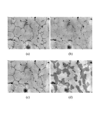
To confirm the role of emerging dislocations, we examined the effect of a field on a vestigial filamentary 360∘ wall structure, such as that shown in Fig. 9. The zero field remnant magnetic pattern obtained after applying a rather large negative field, Oe, but during a short time, depicts an up-magnetized filamentary state. Defects are localized at the end and at the intersection between branches of the filamentary state (Fig. 10a). After applying once again a negative field, Oe (Fig. 10b), branches become far thinner, due to Zeeman forces that partly compensate the dipolar repulsive force between facing walls in the filamentary domains. After switching off the field again to return to a remnant state, the thickness of the new filamentary domains is restored, but a very limited number of up-magnetized branches disappear (compare Fig. 10 a and c). The application of a rather weak positive field ( Oe) blows up the up-magnetized filamentary domains, but preserves bottlenecks at defect positions. This means that the filamentary, or 360∘ domain wall structure, is a highly stable state that is pinned by a small number of defects. Thus, this vestigial filamentary domain structure is clearly initiated and stabilized by point defects, most probably emerging dislocations.
V Conclusion
Magnetization, magneto-transport and PMOKE measurements bring together very consistent data, and enable us to conclude that, albeit the growth on a relaxed (InGa)As buffer, the annealed sample is of high quality, both from the magnetic and transport points of view. These results confirm that (GaMn)As films with perpendicular anisotropy can be grown on a relaxed buffer with nearly the same quality as samples with in-plane anisotropy, grown directly on GaAs. Such good properties allowed to implement PMOKE experiments in optimal conditions for magnetic dynamical and imaging studies. In particular, the magnetization reversal process, which occurs via domain nucleation at rare places followed by fast and quasi-isotropic domain wall propagation, has been observed and interpreted. In spite of the profound difference in the origin of magnetism in metallic and DMS films, micromagnetism and magnetization reversal dynamics show obvious similarities. Emerging dislocations, inherent to growth on a relaxed buffer, form pinning centers for domain walls during the magnetization reversal process at low temperature, giving rise to vestigial filamentary domains, or 360∘ walls. Nevertheless, their low density might allow to fabricate devices, for example to built tunnel junctions with large magnetoresistance or to study current-induced domain-wall propagation in sub-micrometric stripe structures.Yamanouchi et al. (2004)
Acknowledgements.
This work has been supported by the Région Ile de France, the Conseil Général de l’Essonne and through the Action Concertée Incitative BOITQUAN and ANR PNano MOMES. We would like to thank J.-C. Harmand, J.-P. Jamet, and A. Mougin for very fruitful discussions, as well as P. Monod and I. Robert for giving us access to their equipment.References
- Matsukura et al. (2002) F. Matsukura, H. Ohno, and T. Dietl, Handbook of Magnetic Materials (Elsevier, Amsterdam, 2002), vol. 14, p. 1.
- Dietl et al. (2001a) T. Dietl, H. Ohno, and F. Matsukura, Phys. Rev. B 63, 195205 (2001a).
- Ohno et al. (2000) H. Ohno, D. Chiba, F. Matsukura, T. Omiya, E. Abe, T. Dietl, Y. Ohno, and K. Ohtani, Nature 408, 944 (2000).
- Koshihara et al. (1997) S. Koshihara, A. Oiwa, M. Hirasawa, S. Katsumoto, Y. Iye, C. Urano, H. Takagi, and H. Munekata, Phys. Rev. Lett. 78, 4617 (1997).
- Dietl et al. (2001b) T. Dietl, J. König, and A. H. MacDonald, Phys. Rev. B 64, 241201(R) (2001b).
- Sawicki et al. (2004) M. Sawicki, F. Matsukura, A. Idziaszek, T. Dietl, G. M. Schott, C. Ruester, C. Gould, G. Karczewski, G. Schmidt, and L. W. Molenkamp, Phys. Rev. B 70, 245325(R) (2004).
- Thevenard et al. (2005) L. Thevenard, L. Largeau, O. Mauguin, A. Lemaitre, and B. Theys, Appl. Phys. Lett. 87, 182506 (2005).
- Shen et al. (1997) A. Shen, H. Ohno, F. Matsukura, Y. Sugawara, N. Akiba, T. Kuroiwa, A. Oiwa, A. Endo, S. Katsumoto, and Y. Iye, J. Cryst. Growth 175-176, 1069 (1997).
- Edmonds et al. (2002) K. W. Edmonds, K. Y. Wang, R. P. Campion, A. C. Neumann, C. T. Foxon, B. L. Gallagher, and P. C. Main, Appl. Phys. Lett. 81, 3010 (2002).
- Welp et al. (2003) U. Welp, V. K. Vlasko-Vlasov, X. Liu, J. K. Furdyna, and T. Wojtowicz, Phys. Rev. Lett. 90, 167206 (2003).
- Shono et al. (2000) T. Shono, T. Hasegawa, T. Fukumura, F. Matsukura, and H. Ohno, Appl. Phys. Lett. 77, 1363 (2000).
- Pross et al. (2004) A. Pross, S. Bending, K. Edmonds, R. P. Campion, C. T. Foxon, and B. Gallagher, Journ. Appl. Phys. 95, 7399 (2004).
- Hrabovsky et al. (2002) D. Hrabovsky, E. Vanelle, A. R. Fert, D. S. Yee, J. P. Redoules, J. Sadowski, J. Kanski, and L. Ilver, Appl. Phys. Lett. 81, 2806 (2002).
- Moore et al. (2003) G. P. Moore, J. Ferré, A. Mougin, M. Moreno, and L. Daweritz, Journ. Appl. Phys. 94, 4530 (2003).
- Lang et al. (2005) R. Lang, A. Winter, H. Pascher, H. Krenn, X. Liu, and J. K. Furdyna, Phys. Rev. B 72, 024430 (2005).
- Beschoten et al. (1999) B. Beschoten, P. A. Crowell, I. Malajovich, D. D. Awschalom, F. Matsukura, A. Shen, and H. Ohno, Physical Review Letters 83, 3073 (1999).
- Harmand et al. (1989) J.-C. Harmand, T. Matsuno, and K. Inoue, Jap. J. Appl. Physics 28, L1101 (1989).
- Liu et al. (2005) X. Liu, W. L. Lim, L. V. Titova, M. Dobrowolska, J. K. Furdyna, M. Kutrowski, and T. Wojtowicz, Journ. Appl. Phys. 98, 063904 (2005).
- Primus et al. (2005) J.-L. Primus, K.-H. Choi, A. Trampert, M. Yakunin, J. Ferré, J. H. Wolter, W. Roy, and J. D. Boeck, J. Cryst. Growth 280, 32 (2005).
- Sinova et al. (2004) J. Sinova, T. Jungwirth, and J. Cerne, Int. Journ. of Modern Phys. B 18 (2004).
- Berger and Bergmann (1979) L. Berger and G. Bergmann, The Hall Effect and its Applications (Plenum, New York, 1979).
- Jungwirth et al. (2002) T. Jungwirth, Q. Niu, and A. H. MacDonald, Phys. Rev. Lett. 88, 207208 (2002).
- Ferre (2001) J. Ferré, Spin dynamics in confined magnetic structures, (Springer, Heidelberg, 2001), pp. 127–160.
- Hubert and Schäfer (1998) A. Hubert and R. Schäfer, Magnetic Domains (Springer-Verlag, Berlin, 1998).
- Lemerle et al. (1997) S. Lemerle, J.Ferre, A.Thiaville, S. McVitie, and C. Chappert, Kluwer Acad. Publ. pp. 537–542 (1997).
- Yamanouchi et al. (2004) M. Yamanouchi, D. Chiba, F. Matsukura, and H. Ohno, Nature 429 (2004).