Giant Anisotropic Magneto-Resistance in ferromagnetic atomic contacts
Abstract
Magneto-resistance is a physical effect of great fundamental and industrial interest since it is the basis for the magnetic field sensors used in computer read-heads and Magnetic Random Access Memories. As device dimensions are reduced, some important physical length scales for magnetism and electrical transport will soon be attained. Ultimately, there is a strong need to know if the physical phenomena responsible for magneto-resistance still hold at the atomic scale. Here, we show that the anisotropy of magneto-resistance is greatly enhanced in atomic size constrictions. We explain this physical effect by a change in the electronic density of states in the junction when the magnetisation is rotated, as supported by our ab-initio calculations. This stems from the ”spin-orbit coupling” mechanism linking the shape of the orbitals with the spin direction. This sensitively affects the conductance of atomic contacts which is determined by the overlap of the valence orbitals.
pacs:
PACS numbers: 75.70.Kw, 72.75.GdThe effect of an external field on the resistivity of pure ferromagnetic metals (the magnetoresistance-MR) was the subject of intense research work in the second half of the 20ieth century. The field has seen a renewed interest in the past fifteen years with the discovery of giant effects in systems combining magnetic and non-magnetic materials. This Giant Magneto-Resistance (GMR) has had a tremendous impact both through its industrial applications as read-heads and Magnetic Random Access Memories as well as for triggering the field of ”spintronics” barthelemy02 , aiming to use the spin of the charge carriers in electronic devices with higher functionalities. As the pressure towards miniaturization increases, it is important to understand how magnetoresistive effects are influenced by size reduction. In constrictions of dimensions close to the Fermi wavelength, boundary conditions enforce that transverse electronic modes are quantized which results in the discreteness of propagating electron modes. 2-D electron gases are archetypical systems in which the conductance is quantized in units of . In metals where the Fermi wavelength is typically 3 Å, one needs to reach atomic dimensions in order to observe such effects agrait03 . But because even in the single atomic regime several orbitals overlap, one normally finds that several conduction channels are opened with imperfect transparency, i.e. each channel has a transmittance associated to it (a coefficient between 0 and 1). Calculations seem to indicate that 4 or 5 channels participate significantly to the conduction of 3d transition metal nanocontacts smogunov03 ; bagrets04 . The magneto-resistance obtained when one side of the contact flips its magnetization is enhanced compared to that in the bulk bagrets04 ; palacios04 and values of the order of 20% have been reported in some careful experiments viret02 ; yang04 . On the other hand, one could expect some dependence of the conductance to the direction of the magnetization because changing the spins’ direction will affect the orbitals through a mechanism known as spin-orbit coupling. One can describe this interaction by a term in the system’s Hamiltonian written where is called the spin-orbit constant, and are the orbital momentum and spin vectors. In a solid, molecular orbitals lose most of their angular momentum, an effect known as ”quenching”. As a result, the resistance variation with the angle between the local moments and the electrical current lines: the Anisotropic Magneto Resistance (AMR), is only at most a few percent. This is actually the oldest known magnetic effect on electronic transport in ferromagnets,which was discovered in 1857 by W. Thomson ThomsonAMR . When the dimensionality of the system is reduced, like in mono-atomic wires, orbital moments are much larger than in the bulk gambardella02 . One can then expect spin-orbit mechanisms, like the AMR, to be enhanced. Unfortunately, it is extremely difficult to study electrical transport in these systems because one needs to contact tiny structures, a task that often turns out to be impossible.
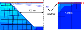
Among the techniques suitable for studying electronic transport in reduced dimensions, break junctions represent an interesting option, because they provide an easy way to drive a current through only a few atoms. The measurement methods we used are based on the breaking of a nanoscopic structure in a controlled manner while monitoring its resistance vanruitenbeek96 . The setup is particularly stable since most of the structure is attached to the substrate and only the narrow bridge to be broken is suspended. It is then possible to mechanically stabilize the contact with a precision of a few picometres. We have slightly modified this procedure and decided not to suspend the bridge, because in ferromagnetic materials, any unsupported part is subjected to a magnetically induced distortion called magnetostriction. This effect results in a modification of the contact geometry when the magnetization changes direction, which has been shown to significantly affect the contact resistance Gabureac04 . This difference in the bridge fabrication is essential here as it proves to be very efficient to reduce magneto-mechanical effects. Fig. 1 shows the result of a finite elements numerical simulation where a 20nm Fe layer is deposited on a kapton substrate with and without the under-etching procedure. Taking the physical parameters for the two materials and a saturation magnetostriction of polycrystalline iron of , the distortion of the Fe layer at the contact level goes from when the bridge is suspended to when the structure is attached to the kapton (no under-etching). We have checked that even in the tunnelling regime (where R changes exponentially with the gap), the effect is negligible. Direct forces due to stray fields are also found to be two orders of magnitude smaller. In fact, any variation in the temperature of the electrodes would have a greater consequence than the magneto-mechanical effects. Therefore, the procedure insures that, in applying a saturating rotating field, the resistance change is only due to the intrinsic anisotropic ”AMR” effect.
We have carried out an extensive set of measurements on Fe break junctions (similar results are also obtained for Ni and Co), where a 2.5 T magnetic field is rotated in the plane of the contact while the resistance is monitored. Interestingly, the resistance and the amplitude of its angular change did not significantly depend on the field magnitude between 0.5 and 2.5 T, where magnetostriction is expected to change by about 50%. This provides further experimental evidence that the effect can be neglected. In order to measure changes of resistance with magnetization direction, a high field was chosen to make sure the atomic contact is always in its saturated state (the demagnetization can be large in nanostructures).
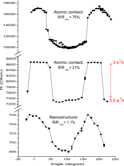
Figure 2 shows a representative set of curves in Fe at 4.2 K. Interestingly, a behaviour qualitatively different from the dependence of the bulk, can be observed in the atomic contact regime. In the middle graph, it looks likely that one channel gets blocked when the field is along the contact, leading to a two-level conductance and an atomic-AMR (AAMR) effect of 21%. At slightly different values of conductance, both smooth sinusoidal variations as well as discrete jumps are observed (see top graph). This is to be expected when overlap changes are not sufficient to completely close a channel, but enough to change their transmittance. This general behaviour is consistent with what is known to happen for non magnetic break junctions when orbital overlap is varied by mechanical deformation of the contacts Scheer98 . There, theoretical calculations have shown that both sharp jumps and smooth variations of the conductance can be explained by considering the details of orbitals overlap Cuevas98 .
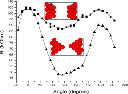
Even more surprising, is the effect measured in tunnelling and shown in figure 3. In this regime, charge carriers jump from one electrode to another through a very narrow vacuum gap (a few Åat most in break junctions). There, the evanescent wave functions still have a strong atomic orbital character from which they can inherit the spin-orbit coupling properties. Moreover, because of the exponential decrease of the wave intensity with distance and the corresponding exponential increase of resistance, it is likely that any change in the shape of the orbitals could have a more significant effect. This is indeed what we experimentally observe. Interestingly, the two measurements shown in Fig.3 correspond to electrons tunnelling through gaps of different sizes (as measured in our setup) and similar resistance. Hence, the tunnelling cross section must differ which implies that electrons tunnel from sharp tips and small gap or flat tips and large gap. The atomic orbital character of the evanescent waves is obviously stronger in the first case, and one can expect the tunnelling-AMR (TAMR) to be larger, as measured. Moreover, because evanescent d orbitals are generally shorter range than s orbitals their contribution should be larger for narrow gaps.
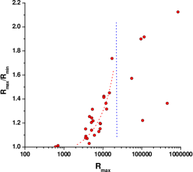
The measured ratio of high to low resistances (when rotating the field) for a Fe sample in different atomic configurations are gathered in figure 4. This plot is instructive because it shows that the AMR effect increases steeply as the contact reaches atomic dimensions. For higher resistances (above ), when in the tunnelling regime, we observe a significant scatter in the amplitude of the TAMR where values around 100% can be achieved but effects as low as 20% can also be found. As explained above, this can be understood because the atomic orbital character of the evanescent waves depends on the exact atomic configuration, which can vary appreciably at constant resistance.
Theoretically, a considerable amount of work has been devoted to metallic atomic contacts, but magnetism has seldom been considered. Most relevant works have studied the resistance generated by a ”magnetic domain wall” on the contact smogunov03 and very recently, the contribution from the exchange splitting has been found to be rather small bagrets04 , the dominating effect being instead the orbital nature of the conduction electrons palacios04 . In order to understand the origin of AAMR effect, we have performed ab-initio calculations to determine the changes of the electronic band structures with the spins direction. In an effort to give a pedagogical illustration of the phenomenon, we consider an ideal atomic chain of Fe atoms. The electronic structure of the wire is obtained using the pseudo-potential plane-wave method implemented in the PWscf package PWSCF which, in its last version, allows to include spin-orbit interactions. Due to the use of plane waves, the system considered is in fact a periodic array of atomic chains, for which the distance between two wires is large enough (15 Å) to avoid interactions. We have first carried out ultrasoft pseudo-potential calculations without spin-orbit in the Generalized Gradient Approximation (GGA) to obtain an equilibrium spacing of the atoms in the wire of Åand a magnetic moment of 3.3 per atom. Then using a fully relativistic (i.e solving the Dirac equation for an atom) ultrasoft pseudo-potential including spin-orbit coupling dalcorso05 in the Local Density Approximation (LDA) we have calculated the electronic structure of the wires with a lattice spacing of .
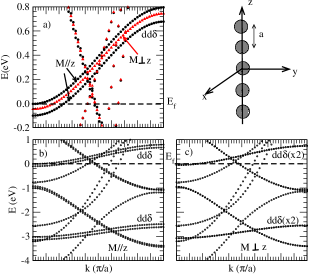
Fig. 5 shows the band structure obtained for the magnetization parallel and perpendicular to the chain. Significant changes near the Fermi level are observed, which stem from the degeneracies induced by spin-orbit coupling. The interesting bands are the weakly dispersive, so called Slater Koster bands, which have a pure (and ) character since they couple neither to and nor to other states with different symmetry. It is clear from Fig. 5 that these bands split by about 0.10 to 0.12 eV when the magnetization is rotated from perpendicular to parallel to the atomic wire. It can actually be shown in a tight-binding model MCD_DS_TB that the splitting is equal to , which leads to a value of . Because these states cross the Fermi level, they will play an important role in defining conduction channels with some transmittance. Since they are also very sensitive to the magnetic orientation, a magnetoresistance effect can be expected. Indeed Fig. 5 shows that when the magnetization is perpendicular to the chain the two degenerate bands are crossing the Fermi level () while in the parallel case their splitting pushes the upper band to higher energies where it hardly touches . This results in a significant electronic transfer which almost empties the upper band. Therefore we can expect a better conductivity when the magnetization is perpendicular to the chain than when it is parallel, in good agreement with the experimental findings. Of course, a direct inference of the conductance from the band structure topology is not possible, but these quantities are intimately linked. What can then safely be said here is that the transmission of some conduction channels will surely change with the magnetization direction. Beyond this simple atomic chain model, we have carried out preliminary tight-binding calculations in a more complex geometry of two pyramids in contact on their apex. The result is that the local density of states at the atoms forming the contact region is also modified when changing the orientation of the magnetization, although a bit less significantly than for the 1-D wire. From these examples, we note that the change in the energy level distribution is complex which could induce a positive or negative AAMR effect, rather sensitive to the atomic, magnetic, and electronic structure at the constriction region. Hence, one can expect the AAMR to depend on the exact atomic geometry as well as the potential difference across the contact. One can even envision sign changes in the AMR with applied voltage.
In conclusion, we have shown that rotating a saturating field in an iron atomic contact leads to significant resistance changes. The effect is due to a spin-orbit coupling induced modification of orbitals overlap. This is supported by ab-initio calculations showing clear changes of the electronic band structure when the orientation of the magnetization in the samples is rotated by 90 °. The AMR effect also exists in the tunnelling regime where evanescent orbitals keep an atomic character. The measured amplitude of the effect opens the possibility of using it in field sensors or magnetic memories of atomic size. We find that the AMR effects (both AAMR and TAMR) are actually larger than the spin scattering effects obtained when the magnetizations are opposite on the two sides of the atomic contact.
Acknowledgements.
It is our pleasure to thank M.C. Desjonquères and D. Spanjaard for fruitful discussions on the tight-binding model and A. Dal Corso for providing a fully relativistic ultrasoft pseudo potential including spin-orbit coupling for Iron. We would also like to thank O. Klein for his experimental help and valuable discussions and X. Waintal for very interesting theoretical conversations.References
- (1) A. Barthelemy et al., J. Mag. Magn. Mat. 242, 68 (2002).
- (2) N. Agraït, A. Levy Yeyati and J.M. van Ruitenbeek, Physics Reports 377, 81-279 (2003).
- (3) A. Smogunov, A. Dal Corso and E. Tosatti, Surf. Science 532-535, 549 (2003).
- (4) A. Bagrets, N. Papanikolaou and I. Mertig, Phys. Rev. B 70, 064410 (2004).
- (5) J.J. Palacios, David Jacob and J. Fernandez-Rossier, cond-mat/0406249 v1 (2004).
- (6) M. Viret et al., Phys. Rev. B 66, 220401, (2002).
- (7) C.-S. Yang, C. Zhang, J. Redepenning, and B. Doudin, Appl. Phys. Lett. 84, 2865 (2004).
- (8) W. Thomson, Proc. Royal Soc. 8, 546 (1857).
- (9) P. Gambardella et al., Nature 416, 301 (2002).
- (10) J.M. van Ruitenbeek et al., Rev. Sci. Instrum. 697, 108 (1996).
- (11) M. Gabureac et al., Phys. Rev. B 69, 100401, (2004).
- (12) E. Scheer et al., Nature 394, 154 (1998).
- (13) J.C. Cuevas, Phys. Rev. Lett 80, 1066 (1998).
- (14) S. Baroni, A. Dal Corso, S. de Gironcoli and P. Giannozzi, http://pwscf.org.
- (15) A. Dal Corso and A. M. Conte, Phys. Rev. B 71, 115106 (2005).
- (16) M.-C. Desjonquères and D. Spanjaard, private communication.