Kinetic stabilization of Fe film on -GaAs(100)
Abstract
We grow Fe film on -GaAs(100) at low temperature, ( K) and study their chemical structure by photoelectron spectroscopy using synchrotron radiation. We observe the effective suppression of As segregation and remarkable reduction of alloy formation near the interface between Fe and substrate. Hence, this should be a way to grow virtually pristine Fe film on GaAs(100). Further, the Fe film is found stable against As segregation even after warmed up to room temperature. There only forms very thin, thick interface alloy. It is speculated that the interface alloy forms via surface diffusion mediated by interface defects formed during the low temperature growth of the Fe film. Further out-diffusion of both Ga and As are suppressed because it should then proceed via inefficient bulk diffusion.
Fe film on GaAs(100) has been extensively studied as a representative system for ferromagnetic metal-semiconductor heterostructure.Prinz Due to the small lattice mismatch () between the double of the lattice constant of Fe and that of GaAs, epitaxial growth of Fe film on GaAs(100) is achieved. However, alloy formation near the interface and serious outdiffusion of both Ga and As from the bulk have been notorious problems.Ruckman ; Chambers ; Kneedler There have been various attempts to solve those problems such as S-passivation of GaAs surface Anderson and insertion of Er layer between Fe and GaAsSchultz . For both cases, the interfacial reaction is reduced to some extent, but the segregated As is still observed. Chye et al.Chye grow Fe film on GaAs (100) at 120 K and also insert Al interlayer. They find improved squareness in magnetic hysteresis and reduced interface states in photo-luminescence spectra. However, no direct investigation on atomic and chemical structure of the Fe film is made.
In the present work, we grow Fe film on GaAs(100) around 130 K, and examine the possibility of kinetic stabilization of the Fe film by photoelectron spectroscopy. Here, we report direct evidence for the effective suppression of the outdiffusion of both Ga and As and the minimal formation of the interface alloy during the growth of the Fe film. When the film is warmed up to room temperature, there forms very thin alloy limited near to the interface. Further outdiffusion of both Ga and As is, however, still suppressed.
All the experiments are performed at 2B1 beam line of Pohang light source in Korea. It is equipped with an electron energy analyzer and low energy electron diffraction (LEED) optics. The base pressure of the chamber is below Torr. For the substrate, we use Si-doped, n-type GaAs(100). Repeated sputtering and annealing produce clean and well-ordered GaAs substrate; sputtering is made by Ar ion beam of 0.5 K eV, with its incidence angle 45o from surface normal to minimize surface damage. Annealing is made at 840 K for 30 minutes. As-prepared surface shows well-defined 4 2 LEED pattern.
We use an e-beam evaporator to deposit Fe film whose thickness is determined by a quartz microbalance that is calibrated by in situ surface x-ray reflectivity (SXR) measurement for thick Fe films. The deposition rate is 0.45 per minute. Temperature of the sample is determined by both an N-type thermocouple and a Si-diode attached near to the sample. Both the deposition of the Fe film and the acquisition of photoelectron spectra are made at the same temperature. All the spectra are taken with a beam energy, 100 eV. Most of the spectra are taken in normal emission geometry, unless otherwise stated.
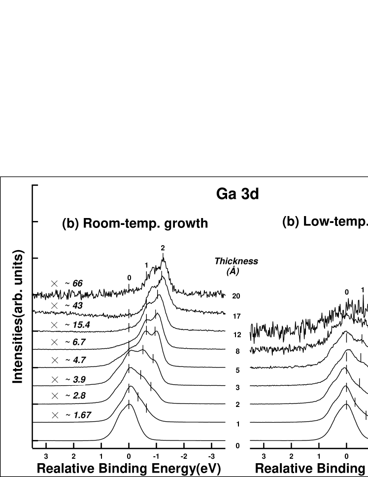
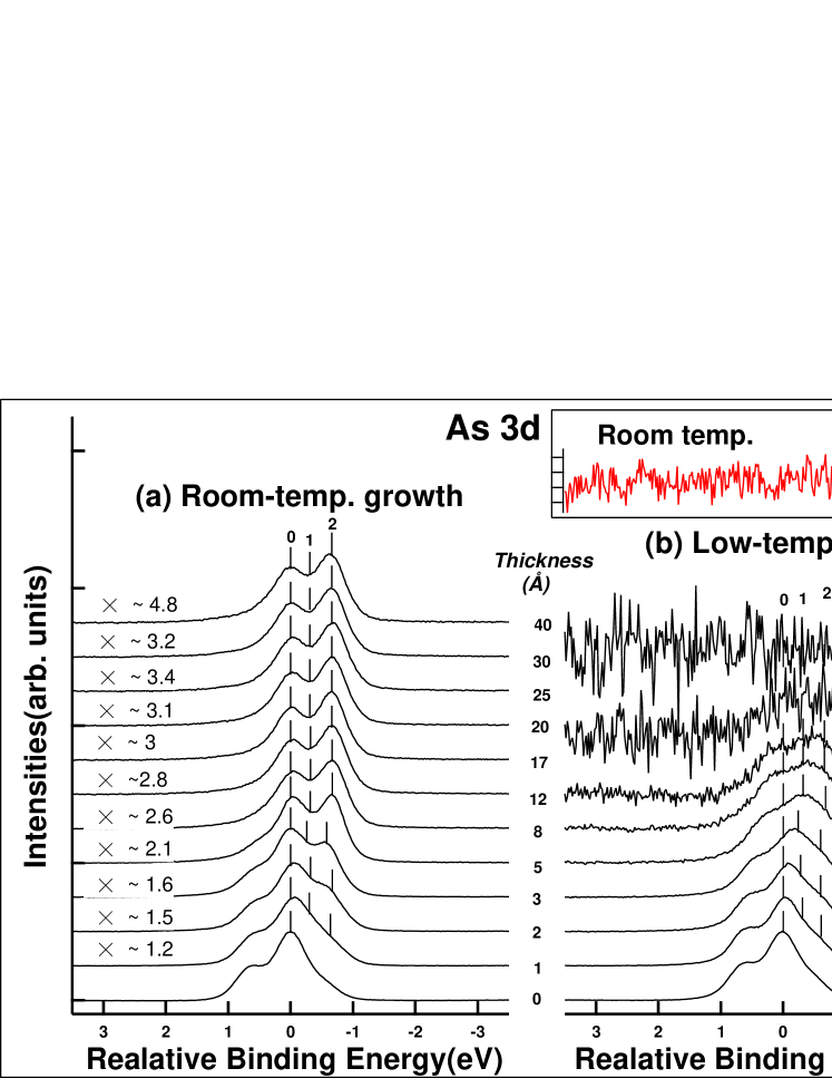
In Fig. 1 and 2, shown are the variations of the spectra for Ga 3d and As 3d with increasing Fe thickness. Each spectrum is normalized to have the same maximum intensity, and vertically shifted for the clear presentation. Binding energies of Ga 3d and As 3d spectra are relative to that of the respective 3d5/2 peak. For the Fe film grown on the substrate at room temperature (RT-grown sample), the peaks for Ga and, especially As 3d are still evident even for the Fe films respectively of 20 for Ga and 40 for As that are much thicker than the escape lengths of the relevant photoelectrons, 3 . It indicates that substantial amount of Ga and As is segregated from the bulk as previously reported.Ruckman ; Chambers ; Kneedler In sharp contrast to the RT-grown sample, for the Fe film grown at low substrate temperature, around 130 K, (LT-grown sample), very rapid decrease of the peak intensities for both Ga and As 3d is observed as the coverage of the Fe film increases. Such an observation strongly suggests that for the LT-grown sample the out-diffusion of Ga and As should be effectively suppressed.
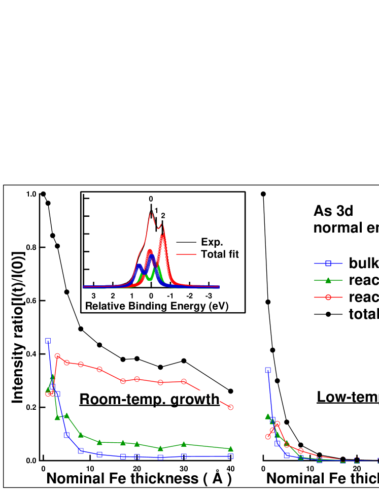
For the quantitative information on the chemical structure of the system, we further analyze the spectra: Each spectrum can be fit by three components, each of which is formed of spin-orbit split two peaks (). (Fig. 3) Similar scheme of fitting was also made by Ruckman et al.Ruckman and Kneedler et al.Kneedler . One difference from their analyses is that Ga 3d spectrum is now fit by three components instead of two, because a broad feature observed in the previous works with its relative binding energy around -0.5 1 eV is now well resolved into two peaks due to improved resolution in the present work (Fig. 1). In the fitting process, we held the Gaussian widths around 0.30.35 eV, but vary Lorentzian width. As an example, we show the fitting results for Ga 3d and As 3d spectra for an Fe film with its thickness of 3, in the inset of Fig. 3 and 4, respectively. The energy difference between and is about 0.45 eV for Ga and 0.69 eV for As. The relative binding energies for the three components of As , 0, 0.3 and 0.6 eV, are similar to the corresponding values, 0, 0.4 and 0.7 eV, determined by Ruckman et al.Ruckman . Those of Ga are slightly different from those of Ruckman et al. due to the increased number of peaks employed for the present fitting as mentioned above.
In Fig.3, summarized is the peak area for each component of Ga 3d as a function of the thickness of the Fe film. For both the RT- and LT-grown samples, the peak areas of the two components(denoted as bulk and reacted 1.) of Ga 3d decreases exponentially. The remaining one (denoted as reacted 2.) initially increases for Fe thickness up to , and then decreases for the RT-grown sample. From those observations, we attribute the first two peaks to the bulk Ga and the Ga adjacent to the Fe film, while the remaining one to Ga forming solid solution with Fe near the interface or interface alloy. A notable difference between the RT-growth and the LT-growth is observed for the interface alloy. In contrast to the RT-grown sample, that component never shows sizable intensity for the LT-grown sample. (Fig. 3) In short, for the RT- grown sample, Ga forms interface alloy with Fe of thickness, while it is almost absent for the LT-grown sample.
Fig.4 shows the peak areas for the three components of As as a function of the thickness of Fe film, respectively for the RT- and LT- grown samples. As for the case of the Ga 3d, for the RT-grown sample, the peak areas of the two components (denoted as bulk and reacted 1.) show exponential decay as the thickness of the Fe film increases. In the thick film limit, the bulk component decreases to show nearly null intensity. That for the reacted 1 reaches a non-zero, but quite low intensity, and tentatively assigned to a solid solution phase of As with Fe film. On the other the remaining one (denoted as the reacted 2.) persists with very large intensity ( 26 of that of bare substrate) even for the Fe film thicker than 40 , and is considered as surface segregated As. This component shows enhanced intensity when the spectrum is taken in 60o off-normal geometry (figure not shown), consistently with the assignment of the component to a surface segregated As. Such segregated As has been previously reported by other groups.Ruckman ; Chambers ; Kneedler
For the LT-grown sample, however, the component corresponding to the segregated As shows disparate behavior or exponential decay of its peak area after initial, short-term (up to 3 of the Fe film) increase. (Fig. 4) The decay length of the total peak area is, however, only , indicating that the outdiffused As is less than 1 ML in regards to the escape depth of the As 3d, . Such an experimental observation tells that the out-diffusion of As can be virtually suppressed by the growth of the Fe film at low substrate temperature, which is here 130 K.
Although the surface segregation and interfacial alloying of Ga and As is dramatically reduced by the LT-growth of Fe film, the thermal stability of the LT-grown sample is an important issue, considering its application for devices whose working temperatures should be mostly around room temperature. For the examination of the thermal stability of the LT-grown Fe film, a LT-grown sample, 30 thick Fe film, is gradually warmed up to room temperature. As 3d peak shows little intensity discernable from the background noise. (Inset of Fig. 2) Moreover, its intensity does not show any enhancement in 60o off-normal emission geometry (figure not shown) either. Thus, we conclude that As does not segregate to the surface at room temperature. Since the probing depth of the photoelectron is limited near to the surface, we still do not know what happens below the surface region. Preliminary results of our surface x-ray reflectivity studysxr finds that upon warming a LT-grown sample, 23 Fe on GaAs(100), to room temperature, there newly forms thick interface alloy. It is speculated that during the annealing process, some substrate atoms diffuse through the vacancies or pinholes near the interface which form in the Fe layers during the low temperature growth. After defects near the interface are exhausted by the substrate atoms, further out-diffusion of them is inhibited, because it should then proceed via bulk diffusion which is much less efficient than the surface diffusion, and hence the LT-grown Fe film is kinetically stabilized.
We grow Fe film on GaAs(001) around 130 K, to kinetically suppress the out-diffusion and the interface alloying of both Ga and As. High resolution photoelectron spectroscopy finds that the interface alloying is limited within several mono-layers from the interface, and the out-diffusion of Ga and especially As is almost suppressed. Such virtually pristine Fe film seems preserved even upon warming the sample up to room temperature, since little spectroscopic change is observed. The thermal stability of the Fe film has kinetic origin; the outdiffusion of the substrate atoms to the Fe film should proceed via bulk diffusion. The kinetically stabilized pure Fe film on GaAs(100) can be widely applicable for the fabrication of devices using ferromagnetic metal-semiconductor junction, especially for the efficient spin injectors.Ploog ; Hanbicki2003
Acknowledgement-This work is supported by KOSEF through CSCMR and by Pohang Accelator laboratory.
References
- (1) G.A. Prinz, in Ultrathin Magnetic Structures II, Eds. B. Heinrich and J.A.C. Bland (Springer-Verlag, Berlin Heidelberg 1994).
- (2) M.W. Ruckman, J.J. Joyce, and J.H. Weaver, Phys. Rev. B 33, 7029(1986)
- (3) S.A. Chambers, F.Xu, H.W. Chen, I.M. Vitomirov, S.B. Anderson, and J.H. Weaver Phys. Rev. B 34, 6605(1986)
- (4) E. Kneedler, P.M. Thibado, B.T. Jonker, B.R. Bennett, B.V. Shanabrook, R.J. Wagner and L.J. Whitman, J. Vac. Sci. Technol. B 14(4) 3193(1996)
- (5) G.W. Anderson, M.C. Hanf, and P.R. Norton, Phys. Rev. Lett. 74, 2764(1995)
- (6) B.D. Schultz, H.H. Farrell, M.M.R. Evans, K. Ldge, C.J. Palmstrm, J.Vac.Sci.Technol.B 20(4), 1600(2002)
- (7) Y. Chye, V. Huard, M.E. White, and P.M. Petroff, Appl. Phys. Lett. 80, 449 (2002).
- (8) T.C. Kim, J.-M. Lee, Y.S. Kim, D.Y. Noh, S.-J. Oh, and J.-S. Kim, (unpublished).
- (9) H.J. Zhu, M. Ramsteiner, H. Kostial, M. Wassermeier, H.-P. Schnherr, and K.H. Ploog, Phys. Rev. Lett. 87, 016601 (2001).
- (10) A.T. Hanbicki, O.M.J. van ’t Erve, R. Magno, G. Kioseolou, C.H. Li, B.T. Jonker, G. Itskos, R. Mallory, M. Yasar, A. Petrou, Appl. Phys. Lett. 82, 4092(2003)