Crosstalk between nanotube devices: contact and channel effects
Abstract
At reduced dimensionality, Coulomb interactions play a crucial role in determining device properties. While such interactions within the same carbon nanotube have been shown to have unexpected properties, device integration and multi-nanotube devices require the consideration of inter-nanotube interactions. We present calculations of the characteristics of planar carbon nanotube transistors including interactions between semiconducting nanotubes and between semiconducting and metallic nanotubes. The results indicate that inter-tube interactions affect both the channel behavior and the contacts. For long channel devices, a separation of the order of the gate oxide thickness is necessary to eliminate inter-nanotube effects. Because of an exponential dependence of this length scale on dielectric constant, very high device densities are possible by using high- dielectrics and embedded contacts.
I Introduction
Much recent experimental and theoretical work has focused on the electronic transport properties of nanowires, motivated by promises of novel electronic devices and the basic scientific challenges that they present. One of the key findings in nanowire devices is that the Coulomb interaction plays a crucial role in determining device properties. For example, electrostatics in carbon nanotubes (NTs) leads to unexpected behavior of intra-tube p-n junctions[1], of intra-tube Schottky junctions[2], and of Fermi level pinning at contacts between NTs and metals[3]. The importance of intra-tube Coulomb interactions naturally leads to the question of how inter-tube interactions might influence device behavior. Answering this question is gaining increasing importance as experimental devices based on multiple nanotubes are becoming more common[4, 5, 6, 7] [an example is shown in Fig. 1(a)], and also to address the question of device packing density.
In this paper, we present self-consistent calculations based on the non-equilibrium Green’s function technique for planar carbon nanotube transistors containing multiple parallel NTs. By analyzing the variations of the transistor characteristics with NT separation, we establish a length scale below which inter-tube interactions become important. While for small channel lengths this length scale depends on the channel length, for long channel devices it becomes independent of the channel length and is essentially determined by the gate oxide thickness. Importantly, this length scale depends exponentially on the dielectric constant of the medium surrounding the NTs, and can be substantially reduced by embedding the NTs in a high- dielectric in the channel and using embedded contacts.
II Computational approach
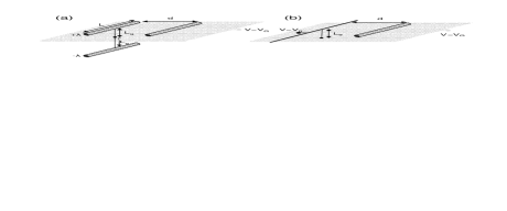
Figure 1(b-e) shows the device under consideration: infinitely long single-wall zigzag NTs laying on metal electrodes at their two ends and on a dielectric in the channel region. A planar gate 10 nm below the dielectric surface controls the device behavior. We take a spacing of 0.3 nm between
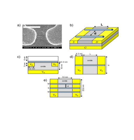
the NT and the metal or dielectric, and assume that the NT cross-section remains circular, a good approximation for the NTs considered here[8]. The electronic properties of the NT are described using a tight-binding approach with one orbital per carbon atom, and a coupling eV between nearest-neighbor atoms. Semiconducting tubes are (17,0) NTs (band gap of 0.55 eV, diameter of 1.33 nm) while metallic tubes are (18,0) NTs (diameter of 1.41 nm). We take the NT midgap as the energy reference level, and use a metal workfunction of 5.5 eV, putting the metal Fermi level 1 eV below the NT midgap. The gate insulator dielectric constant is that of SiO
To apply the non-equilibrium Green’s function formalism[9, 10] to this system, we divide the NT in principle layers, with each layer corresponding to a ring of the zigzag NT. The main quantity of interest is the Green’s function , from which one can obtain the transmission probability and the zero bias conductance
| (1) |
where is the Fermi function. is calculated by solving the matrix equation
| (2) |
where is the tight-binding Hamiltonian for the isolated NT and is the electrostatic potential evaluated at the position of each layer. The functions and represent the interaction of the scattering region with the semi-infinite NT leads. In our tight-binding representation, the Hamiltonian matrix elements for layer are , where is the number of atoms around a NT ring ( or here) and labels each of the NT bands. In this representation, we assume that the electrostatic potential on every atom of a ring is the same, a good approximation in this case since varies slowly over the NT diameter.
The electrostatic potential is calculated by solving Poisson’s equation in three-dimensional coordinates on a variable grid with the source charge on the NT, and with boundary conditions at the source, drain, and gate surfaces, and at the vacuum/dielectric interface. This is done by combining a finite difference approach in the directions parallel to the NT and perpendicular to the substrate with a fast fourier transform in the direction perpendicular to the NTs. Once the three-dimensional electrostatic potential is obtained, the value for on each ring is taken as the average of the electrostatic potentials on the points on the NT nearest and furthest from the substrate, at the position of each ring.
To obtain the charge density, we note that our tight-binding technique provides the total charge on each layer of the NT, which needs to be spatially distributed. We assume a uniform distribution of the charge in the azimuthal direction, and spatially distribute the total charge in the radial and axial directions with a Gaussian smearing function. The three-dimensional charge density is then given by
| (3) |
where with the tube radius, the position of ring , and and the smearing lengths in the axial and radial directions respectively (this expression for is valid when , and we used values of nm and nm). Our overall procedure is to solve the coupled set of nonlinear Eqs self-consistently for a given gate-source voltage at zero drain-source bias. Figure 1(e) shows the unit cells for our calculations to study semiconducting-semiconducting and semiconducting-metallic interactions.
III Results and discussion
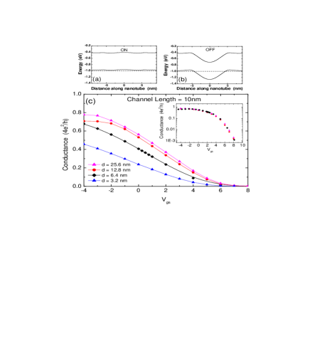
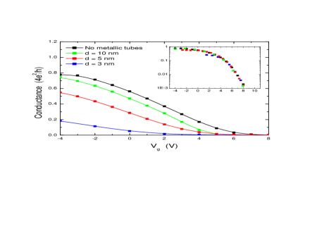
We first discuss interactions between semiconducting NTs. The conductance of the NT transistor as a function of the gate-source voltage is plotted in Fig. 2 for different values of the separation between the NTs. Clearly, as the NT separation is reduced, the NTFET characteristics degrade; in the range of gate voltages studied, the current cannot be completely turned on for the smallest tube separation, while the behavior in the OFF state is essentially independent of tube separation. This behavior arises because of the charge induced on the NTs by the gate voltage, and by interactions between NTs at the contact. As shown in Fig. 2a, the OFF state corresponds to the Fermi level in the middle of the NT bandgap in the channel, with little charge on the NTs, so Coulomb interactions in the channel between neighboring NTs are negligible. The ON state however consists of making the NT p-type in the channel by raising the valence band above the Fermi level with the gate voltage (Fig. 2b); this creates a large positive charge on the NT which interacts with the charge on neighboring NTs, and lowers the electron energy. This pushes the bands down, and reduces the conductance.
While interactions in the channel play an important role in determining device behavior, NT-NT interactions also affects the contacts. Because of the mismatch between the metal and NT workfunctions, contacts between NTs and metals are governed by charge transfer between the metal and the NT, effectively doping the NT p-type at the contact, with the metal Fermi level just below the NT valence band edge in the contact[11]. As the separation between NTs decreases, the Coulomb interactions between the positive charge at the contacts leads to a lowering of the bands; at small enough separations, the valence band in the contact can be pushed below the metal Fermi level. Thus inter-tube interactions at the contacts can lead to modifications of the NT/metal contacts from ohmic to Schottky. We find that this effect becomes important for inter-tube separations below nm; the effects can be seen in the bottom curve of Fig. 2, where the ON state conductance saturates to a value much smaller than the single-tube limit because of the Schottky barrier. These effects of inter-tube interactions on contact properties can be mitigated by embedding the NTs in the metal contact.
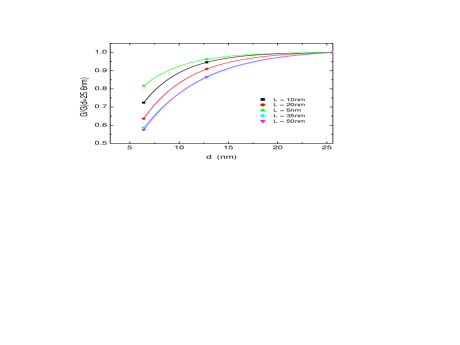
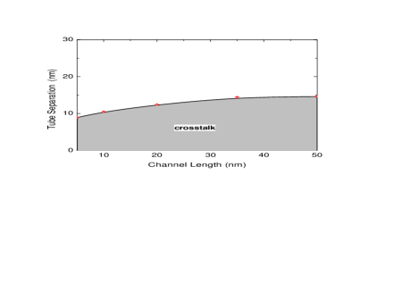
To quantify the role of Coulomb interactions in the channel, we calculated the conductance versus gate voltage for devices with different channel lengths; we plot in Fig. 3 the conductance at versus tube separation, for several values of the channel length (the smallest value of is large enough to avoid contact effects). The solid lines in the figure are fits of the form , from which we extract the value of at which the conductance decreases by more than 10% from its value. This length scale is plotted in Fig. 4 as a function of channel length, and delimits regions where inter-tube interactions distort the single-tube behavior. Clearly, very short channel devices can have very high packing densities, while long channel devices are limited to tube separations of 15 nm. A notable aspect of the results of Fig. 4 is that the value of is independent of the channel length for large . At first glance, one would expect that a larger channel length leads to larger total charge on the NTs and thus larger interaction energy. However, screening of the Coulomb interaction by the planar gate leads to a different behavior, as we now discuss.
To derive approximate analytical expressions for the Coulomb interactions between NTs, we consider the simplified situation of Fig. 5a: a NT of length is at a distance above a metallic substrate held a potential , and carries charge per unit length . We use an image potential construction to calculate the electrostatic potential at a distance from the charged tube, giving
| (4) |
In the long channel limit , Eq. (4) becomes
| (5) |
The important point here is that in this limit the potential shift is independent of the channel length . Taking a potential change of Volts as a criterion for the importance of inter-tube effects, we obtain a separation
| (6) |
below which inter-tube effects become important. Thus the gate oxide thickness sets the length scale . In the above expression, is the effective dielectric constant for the device geometry. For a simple comparison with our simulations we take as the dielectric constant of SiO2, and use the computed value of e/C atom in the ON state. This gives nm in good agreement with our numerical results. A key point is that the length scale depends exponentially on the gate insulator dielectric constant; thus, replacing SiO2 with high- dielectric materials (NTFETs have been fabricated with HfO2[12], SrO2[13] and SrTiO3[14]) allows a reduction of to extremely small values, thus permitting high device densities.
The general behavior of interactions between semiconducting NTs can be understood from further analysis of Eq. . Near threshold, the charge on the NT can be written as where is the threshold voltage. Substitution in Eq. gives
| (7) |
Hence, the gate voltage is rescaled and shifted by the interaction between NTs. This behavior is indicated in the inset of Fig. 2c, showing good collapse of the data after appropriate rescaling and shifting of .
The results discussed above focused on interactions between semiconducting NTs. However, in multi-NT devices, there is often a mixture of semiconducting and metallic nanotubes. A question therefore is how the presence of nearby metallic NTs affects the properties of the semiconducting NTs. To address this issue, we performed calculations for the geometry depicted in Fig. 1(e). There, a semiconducting NT is separated from two metallic NTs by a distance . Figure 6 shows the calculated conductance vs gate voltage dependence for a 10 nm channel device. (The conductance plotted here is that of the semiconducting NT only. For single electrodes making contact to all the NTs, the conductance of the metallic tubes would have to be included to obtain the total device conductance.) The behavior in Fig. 6 is similar to that observed for interactions between semiconducting NTs, i.e. a degradation of the characteristics with decreasing separation between the NTs. However, because the charge on the metallic tubes is not strongly modulated by the gate voltage, the physics is somewhat different; indeed, the metallic NTs essentially consist of lines of constant potential. To their effect on the semiconducting NTs we consider the situation of Fig. 5b, where a line held at a constant potential is above a metallic plane held at potential . Solution of the Laplace equation for this geometry gives the potential on the nearby NT as
| (8) |
Thus the presence of the metallic tubes shifts and rescales the gate voltage seen by the semiconducting tube. For small separations between the NTs, the potential on the semiconducting NT approaches that of the metallic NT, which is larger than that of an isolated semiconducting NT. Thus, at the contact, the Fermi level is pushed above the valence band edge, leading to a Schottky barrier and saturation of the conductance to lower values. The behavior expressed in Eq. (8) can be verified by looking at the OFF state behavior, and scaling and shifting the gate voltage appropriately; the inset in Fig. 6 shows the resulting collapse of the data.
IV Conclusion
In summary, we have shown that Coulomb interactions between carbon nanotubes can have a strong influence on device behavior. Below a characteristic length scale, interactions between NTs can significantly degrade device behavior; this can be understood in terms of a rescaling and shift of the applied gate voltage. For long channel devices, the tube separation above which interactions between NTs is negligible becomes independent of the channel length, and is set by the gate oxide thickness. This length scale can be substantially reduced by using high- dielectrics, due to an exponential dependence on dielectric constant. While this paper focused on the static device properties, we expect that interactions during current flow (e.g. Coulomb drag) would also have intriguing properties. We hope that this work will stimulate controlled experiments to further explore interactions between nanotubes.
Acknowledgments
Sandia is a multiprogram laboratory operated by Sandia Corporation, a Lockheed Martin Company, for the United States Department of Energy under contract DE-AC01-94-AL85000. We thank K. McDonald, F. Jones, and A. Talin for providing the SEM image in Fig. 1.
REFERENCES
- [1] Léonard F and Tersoff J 1999 Phys. Rev. Lett. 83 5174
- [2] Odintsov A A 2000 Phys. Rev. Lett. 85 150
- [3] Léonard F and Tersoff J 2000 Phys. Rev. Lett. 84 4693
- [4] Star A, Gabriel J-C P, Bradley K and Grüner G 2003 Nano Lett. 3 459
- [5] Snow E S, Perkins F K, Houser E J, Badescu S C and Reinecke T L 2005 Science 307 1942
- [6] Li J, Lu Y, Ye Q, Cinke M, Han J and Meyyappan M 2003 Nano Lett. 3 929
- [7] Dimaki M and Bøggild P 2005 Nanotechnology 16 759
- [8] Hertel T, Walkup R E and Avouris Ph 2002 Phys. Rev. B 58 13870
- [9] Datta S Electronic transport in mesoscopic systems (Cambridge University Press, Cambridge, England 1995).
- [10] Léonard F 2002 Proc. Intl. Conf. Comput. Nanoscience 1 298
- [11] Léonard F and Tersoff J 2002 Phys. Rev. Lett. 88 258302
- [12] Javey A, Guo J, Former D B, Wang Q, Wang D W, Gordon R G, Lundstrom M and Dai H J 2004 Nano Lett. 4 447
- [13] Javey A, Kim H, Brink M, Wang Q, Ural A, Guo J, Mcintyre P, McEuen P, Lundstrom M and Dai H 2002 Nature Materials 1 241
- [14] Kim B M, Brintlinger T, Cobas E, Fuhrer M S, Zheng H M, Yu Z, Droopad R, Ramdani J and Eisenbeiser K 2004 Appl. Phys. Lett. 84 1946