Electrical contacts to nanotubes and nanowires: why size matters
Abstract
Electrical contacts to semiconductors play a key role in electronics. For nanoscale electronic devices, particularly those employing novel low-dimensionality materials, contacts are expected to play an even more important role. Here we show that for quasi-one-dimensional structures such as nanotubes and nanowires, side contact with the metal only leads to weak band re-alignement, in contrast to bulk metal-semiconductor contacts. Schottky barriers are much reduced compared with the bulk limit, and should facilitate the formation of good contacts. However, the conventional strategy of heavily doping the semiconductor to obtain ohmic contacts breaks down as the nanowire diameter is reduced. The issue of Fermi level pinning is also discussed, and it is demonstrated that the unique density of states of quasi-one-dimensional structures make them less sensitive to this effect. Our results agree with recent experimental work, and should apply to a broad range of quasi-one-dimensional materials.
The early work of Schottky, Mott and Bardeen has laid the course for much of the fundamental understanding and improvement in the performance of electrical contacts to bulk semiconductors. For nanoelectronics, contacts are a significant fraction of the total device size and are expected to be crucial for device behavior. However, because of the unique properties of nanostructures, much of the basic fundamental aspects of contacts need to be re-examined at the nanoscale.
The current understanding of contacts to nanostructures is in its infancy, both from an experimental and theoretical perspective. An example is carbon nanotubes (NTs): despite much experimental work, it is still unclear wether the contacts are Schottky or ohmic, with reports of Schottky contacts for Ti[1] and ohmic contacts for Au[2] and Pd[3, 4]. However, recent experimental work[5, 6] has suggested that the type of contact depends on the NT, with Schottky contacts for small diameter NTs and ohmic contacs for large diameter NTs.
From a theoretical perspective, it has been demonstrated that the concept of Fermi level pinning (crucial in traditional semiconductors) is ineffective for quasi-one-dimensional nanostructures end-bonded to metals[7]. For NTs side-contacted by a metal, modeling has been used to extract Schottky barriers from experimental measurements of the ON current in NT transistors[5], but have not addressed the origin of the Schottky barriers; and atomistic calculations have provided case-by-case studies[8, 9] for planar contacts. However, a more general theoretical understanding for side-contacts to quasi-one-dimensional (Q1D) structures is still missing, especially in light of the recent experimental findings.
In this paper, we present a theoretical and modeling analysis of side contacts to nanotubes and nanowires. We show that the conventional concepts developed for bulk metal-semiconductor contacts do not simply carry over to the nanoscale. In particular, band re-alignement due to charge transfer is weak due to the limited available depletion width. In NTs, this leads to relatively small and slowly varying Schottly barriers with NT diameter. In nanowires (NWs), there is a range of diameters with minimized Schottky barriers, providing optimal contact properties. We also demonstrate that in general, Q1D structures are much less sensitive to Fermi level pinning than their bulk counterparts. Finally, a conventional strategy for making ohmic contacts is to heavily dope the semiconductor near the contact; we show that at typical dopings for Si, the contact resistance increases rapidly as the nanowire diameter is decreased below 40 nm.
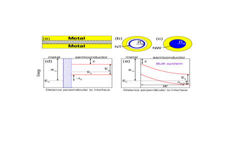
We begin by describing the contact geometry considered here. Figure 1a shows a sketch of a cross section of the contact consisting of a Q1D structure embedded in a metal. For explicit systems, we consider a single-wall NT , as shown in Fig. 1b, or a solid nanowire as in Fig. 1c. For the NT, the metal forms a cylindrical cavity of radius where is the NT radius and is the distance between the NT and the metal, while for the NW we consider a solid, continuum cylinder embedded in a perfect metal, with a sharp interface between the nanowire surface and the metal.
In the simplest picture, the difference between the metal Fermi level and the semiconductor valence band edge (the barrier for holes) is simply given by (Fig. 1d)
| (1) |
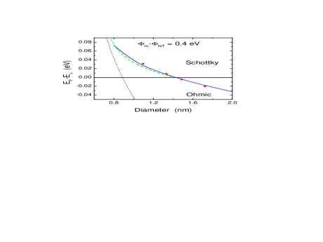
where and are the metal and semiconductor workfunctions respectively, and is the semiconductor band gap. A positive value for indicates a Schottky barrier, while a negative value indicates an ohmic contact. Because bandgap decreases with increasing diameter for Q1D structures, the value of depends on the nanostructure diameter. The behavior of Eq. for undoped NTs is shown in Fig. 2 for a value of eV (typical of Pd), and using the relation between bandgap and NT diameter ( nm is the C-C bond length and eV is the tight-binding overlap integral). One problem with this picture (besides the fact that the physics is incomplete, as will be discussed below) is that Eq. predicts large and negative values for signaling strong ohmic contacts. However, it is clear that such strong ohmic contacts are not observed experimentally.
In general, because the metal Fermi levels of the metal and semiconductor are not equal, charge transfer between the metal and semiconductor occurs, and leads to band re-alignement. At a bulk semiconductor junction (Fig. 1e) this charge transfer leads to the Schottky barrier
| (2) |
where is the semiconductor electron affinity. This relationship arises because, in the bulk system, a depletion width perpendicular to the metal-semiconductor interface is created in the semiconductor until the band lineup in Eq. is obtained. However for Q1D structures, the depletion width depends exponentially on the doping[10] and is much longer than the device size for non-degenerate doping, leading to slowly varying bands outside of the contact; and for a three-terminal device the band-bending in the channel is governed by the gate voltage. In either case, the band alignment is determined by that in the contact. But for a side-contacted Q1D structure, the semiconductor is only a few nanometers thick in the direction perpendicular to the metal-semiconductor interface; thus only a region of the order of the nanostructure cross-section can be depleted, giving partial band re-alignement. The value of will then be somewhere between and (for an undoped NT or NW, which would always give relatively high Schottky barriers).
Nanotubes are an extreme example of this situation, since the possible “depletion width” is the size of the NT wall; the charge transfer and image charge in the metal create two nested hollow cylinders with opposite charge, and an associated electrostatic potential. This electrostatic potential in turn shifts the bands, and changes the amount of transferred charge. Thus, the charge and potential must be determined self-consistently. We can capture this behavior using analytical models for the charge and potential. The charge per unit area on the NT can be expressed as
| (3) |
where
| (4) |
is the NT density of states[11], is the Fermi function, and is the atomic areal density. We assume a uniform and sharp distribution of the charge on the NT.
For the geometry of Fig. 1, solution of Poisson’s equation gives the potential on the NT as
| (5) |
where is the permittivity of free space and is the capacitance per unit area between the metal and the NT. Equations and can be solved self-consistently for a given NT. In this model the electrostatic potential induced on the NT modifies the barrier to
| (6) |
Figure 2 shows results of such calculations for parameters typical of Pd. Clearly, the behavior is different from the simple expressions in Eqs and . The results suggest that there is a transition between Schottky and ohmic behavior at a NT diameter around 1.4 nm, in agreement with recently published experimental data for Pd contacts[5, 6].
The results of these calculations can be verified using an atomistic treatment of the NT. For selected zigzag NTs, we apply a tight-binding Green’s function formalism, dividing the system into semi-infinite left and right leads connecting a central scattering region (Fig. 1a). In the central region, we calculate the Green’s function from
| (7) |
where is the tight-binding Hamiltonian for the isolated NT and is the electrostatic potential on each ring of the zigzag NT. The function represents the interaction of the scattering region with the semi-infinite NT leads. To obtain the charge density, we assume a uniform distribution of the charge in the azimuthal direction, and spatially distribute the total charge on each ring in the radial and axial directions with a Gaussion smearing function. Thus the three-dimensional charge density is given by
| (8) |
where with the tube radius, the position of ring , and and the smearing lengths in the axial and radial directions respectively (this expression for is valid when , and we use values of nm and nm).
The electrostatic potential is calculated by solving Poisson’s equation in cylindrical coordinates on a grid with the geometry of Fig. 1. Once the three-dimensional electrostatic potential is obtained, the value for on each layer is taken as the value of the three-dimensional electrostatic potential at the atomic position of each ring along the NT. We iterate the calculation of the charge and the electrostatic potential until self-consistency.
As shown in Fig. 2, the results of such calculations indicate excellent agreement with the analytical approach introduced above. This agreement allows us to use equations and to gain further understanding of the properties of these contacts, as we now discuss.
To proceed further we focus on the small and positive regime, and approximate the fermi distribution as where . Asymptotic expansion of the integral in Eq. 3 leads to the charge
| (9) |
Combined with Eq. this expression for the charge gives the Schottky barrier
| (10) |
where and is Lambert’s W function. A more appealing formula can be obtained using asymptotic expansion of giving
| (11) |
The behavior of this function is plotted in Fig. 2, showing good agreement with the full calculation. The logarithmic dependence implies relatively slowly varying at least compared with Eq. . The NT diameter delimiting Schottky from ohmic behavior is[12]
| (12) |
thus the diameter is increased from its bare value by . Making ohmic contact to a wide range of NT diameters requires a small ; this can be accomplished at low temperature, or with a large metal workfunction. Because is inversely proportional to the capacitance, our result also provides one reason why embedding the NT in the metal and heating can improve the contact properties: the embedded contact provides a larger capacitance compared to a planar contact (for typical parameters we find for the embedded contact and up to for a planar contact), while heating presumably provides a smaller average value for and a smaller capacitance. The large value of for planar contacts imply that this type of contact is almost pathological, since the value of should be very large unless the metal worfunction itself is large. This may explain why ab initio calculations find Schottky barriers[8, 9] despite the large values of used in the calculations. It is worth mentioning that changing the contact geometry to modify the contact properties is not possible in bulk contacts, and is thus a unique feature of nanostructures.
We now consider side-contacts to nanowires. The difference between NWs and NTs is two-fold: first, in NWs the possible depletion width increases with diameter, while in a NT it stays constant; second, while the band gap also decreases with diameter for NWs[13], the large diameter limit can lead to a finite band gap, while for NTs it leads to a zero band gap. It is not clear a priori how these effects influence the contact behavior. To address this issue, we consider a model NW with density of states
| (13) |
where is the effective mass. For silicon NWs, it has been shown experimentally[13] that the band gap depends on diameter as where eV and eVnm2. We consider the situation eV typical of contacts to Si. Fig. 3a shows the expected Schottky barrier heights from Eq. which predicts ohmic contacts to NWs with diameters larger than 4 nm. To study the effects of charge transfer, we perform a self-consistent calculation of the charge and potential, using Eq. to obtain the charge and solving Poisson’s equation numerically in the NW to obtain the potential (we use an atomic volume density atoms/m3).
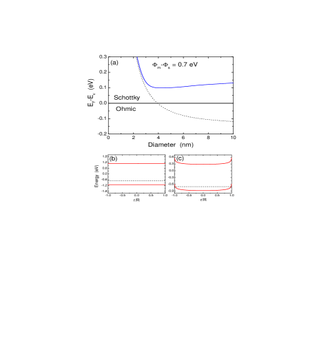
Fig. 3b,c shows the self-consistent band-bending for NWs of 2 and 10 nm radius. Clearly, the nanoscale dimension of the NWs prevents the bands from reaching their asymptotic value; instead, there is only a relatively weak band-bending present. To quantify the Schottky barrier height, we calculate the spatial average of ; the results plotted in Fig. 3a indicate a remarkable behavior: the contact is always of Schottky character, with the barrier minimized at a diameter of about 4 nm. Thus, while in NTs the barrier height decreases monotonically with diameter, the behavior in other Q1D structures may be non-monotonic, with a range of diameters providing optimal contact properties.
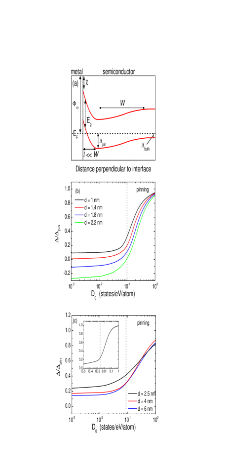
We now discuss the issue of Fermi level pinning. As shown in Fig. 4a, in a bulk metal-semiconductor contact, metal-induced gap states (MIGS) lead to band-bending over a distance , and modification of the Schottky barrier height to . The question is to what extent this mechanism influences the properties of side contacts to NTs and NWs. To model this effect, we consider a radial pinning charge[7]
| (14) |
where the neutrality level is at midgap [i.e. ], for a NW and for a NT, and for a NT and for a NW. We choose nm, a typical value for metal-semiconductor interfaces[14]. We add this pinning charge to Eq. or to the charge calculated from Eq. and repeat our self-consistent calculations.
Figure 4b shows the Schottky barrier calculated for several NTs as a function of the density of gap states (). Clearly, there is a rapid onset of pinning at states/(atomeV); this value of is rather larger considering the van der Waals bonding of NTs to metals. Furthermore, atomistic calculations[8] have obtained values at least an order of magnitude smaller. Thus, as in end-bonded contacts, we expect that Fermi level pinning will play a minor role in side-contacts to NTs. The rather large value of required to see pinning effect is a generic property of Q1D structures as we now discuss.
Figure 4c shows the effects of Fermi level pinning on the barrier height in SiNWs. The results also indicate a value of states/(atomeV) required to see pinning effects. For comparison, the inset in this figure shows the same calculation for a bulk metal-semiconductor interface with the same parameters, indicating that only states/(atomeV) are needed to reach the onset of pinning. Thus, the Q1D system requires almost two orders of magnitude larger density of pinning states compared with the bulk interface.
The origin of this behavior can be traced to the unique density of states of Q1D systems. Indeed, for Si, we can repeat the analysis leading to Eq. using the density of states for the NW and for the bulk system []. This leads to the ratio .
The appearance of the factor in the denominator is entirely due to the Q1D density of states of the NW and the presence of a van Hove singularity at the band edge. At room temperature, we find that ; thus the MIGS are competing with a much larger charge density in the Q1D system.
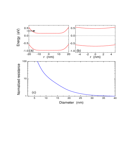
Our discussion has so far focused on the situation of low doping, where the strategy for making ohmic contacts is by selection of a metal with appropriate workfunction. In traditional metal-semiconductor contacts, an alternative approach is to heavily dope the semiconductor, and rely on tunneling through the Schottky barrier to reduce the contact resistance and obtain ohmic-like contatcs. To address the feasibility of this approach for contacts to NWs, we repeat our self-consistent calculations for the Si NW, focusing on the situation where the metal Fermi level is in the middle of the NW bandgap at the interface, and adding a uniform doping charge of . Figure 5 shows the band-bending in the presence of this doping charge for NWs of 40 and 10 nm diameters. We calculate the contact conductance from
| (15) |
where the tunneling probability is obtained from the WKB approximation. The normalized contact resistance is then where is the conductance in the limit of large diameters. The behavior of the normalized resistance as a function of NW diameter is shown in Fig. 5c, indicating a rapid increase of the resistance with decrease in diameter. The origin of this behavior is due to the increased tunneling distance and reduced range of tunneling energies because of the poor band-bending in the NW (the increase in bandgap also plays a role for the smaller diameters). One implication of this result is that different diameter NWs will require different doping levels to achieve the same contact quality.
In summary, we find that the concepts developed to describe traditional metal-semiconductor interfaces fail to properly account for the properties of contacts to quasi-one-dimensional structures such as nanowires and nanotubes. The nanometer cross-section of nanowires and nanotubes prevents the formation of an appropriate depletion width, leading to only weak band re-alignement; and because of the diverging density of states at the band edge, these nanostructures are much less sensitive to Fermi level pinning than their bulk counterparts. Optimizing device performance will not only require selecting Q1D structures for their behavior in the channel, but also for their contact properties. We expect that our results will be applicable to a broad range of Q1D structures.
∗email:fleonar@sandia.gov
Acknowledgement. Sandia is a multiprogram laboratory operated by Sandia Corporation, a Lockheed Martin Company, for the United States Department of Energy under contract DE-AC01-94-AL85000.
REFERENCES
- [1] Heinze, S.; Tersoff, J.; Martel, R.; Derycke, V.; Appenzeller, J.; Avouris, Ph. Phys. Rev. Lett. 2002, 89, 106801.
- [2] Yaish, Y.; Park, J.-Y.; Rosenblatt, S.; Sazonova, V.; Brink, M.; McEuen, P. L. Phys. Rev. Lett. 2004, 92, 046401.
- [3] Javey, A.; Guo, J.; Wang, Q.; Lundstrom, M.; Dai, H. J. Nature (London) 2003, 424, 654.
- [4] Javey, A.; Guo, J.; Former, D. B.; Wang, Q.; Wang, D. W.; Gordon, R. G.; Lundstrom, M.; Dai, H. J. Nano Lett. 2004, 4, 447.
- [5] Chen, Z.; Appenzeller, J.; Knoch, J.; Lin, Y.-M.; Avouris, Ph. Nano Lett. 2005, 5, 1497.
- [6] Kim, W.; Javey, A.; Tu, R.; Cao, J.; Wang, Q.; Dai, H. Appl. Phys. Lett. 2005, 87, 173101.
- [7] Léonard, F.; Tersoff, J. Phys. Rev. Lett. 2000, 84, 4693.
- [8] Xue, Y.; Datta, S. Phys. Rev. Lett. 1999, 83, 4844.
- [9] Shan, B.; Cho, K. Phys. Rev. B 2004, 70, 233405.
- [10] Léonard, F.; Tersoff, J. Phys. Rev. Lett. 1999, 83, 5174.
- [11] Mintmire, J. W.; White, C. T. Phys. Rev. Lett. 1998, 81, 2506.
- [12] To derive this relation we assumed a constant capacitance over the range of NT diameters of interest. A more detailed treatment would not change the key physics.
- [13] Ma, D. D. D.; Lee, C. S.; Au, F. C. K.; Tong, S. Y.; Lee, S. T. Science 2003, 299, 1874.
- [14] Louie, S. G.; Cohen, M. L. Phys. Rev. B 1976, 13, 2461.