Nonlinear Dynamics in the Resonance Lineshape of NbN Superconducting Resonators
Abstract
In this work we report on unusual nonlinear dynamics measured in the resonance response of NbN superconducting microwave resonators. The nonlinear dynamics, occurring at relatively low input powers (2-4 orders of magnitude lower than Nb), and which include among others, jumps in the resonance lineshape, hysteresis loops changing direction and resonance frequency shift, are measured herein using varying input power, applied magnetic field, white noise and rapid frequency sweeps. Based on these measurement results, we consider a hypothesis according to which local heating of weak links forming at the boundaries of the NbN grains are responsible for the observed behavior, and we show that most of the experimental results are qualitatively consistent with such hypothesis.
pacs:
85.25.-j, 74.50.+r, 47.20.Ky, 05.45.-aI INTRODUCTION
Understanding the underlying mechanisms that cause and manifest nonlinear effects in superconductors has a significant implications for both basic science and technology. Nonlinear effects in superconductors may be exploited to demonstrate some important quantum phenomena in the microwave regime as was shown in Refs. squeezing ; JPA , and as was suggested recently in Refs. Yurke ; Eyal . Whereas technologically, these effects can play a positive or negative role depending on the application. On the one hand, they are very useful in a wide range of nonlinear devices such as amplifiers rf driven ; Direct , mixers mixer , single photon detectors single photon , and SQUIDs flux qubit . On the other hand, in other applications mainly in the telecommunication area, such as band pass filters and high Q resonators, nonlinearities are highly undesired Dahm ; RF power dependence ; Intrinsic ; nonlinear dynamics .
Various nonlinear effects in superconductors and in NbN in particular have been reported and analyzed in the past by several research groups. Duffing like nonlinearity for example was observed in superconducting resonators employing different geometries and materials. It was observed in a high- superconducting (HTS) parallel plate resonator Thermally induced nonlinear behaviour , in a Nb microstrip resonator microwave nonlinear effects in He-cooled sc microstrip resonators , in a Nb and NbN stripline resonators nonlinear dynamics , in a YBCO coplanar-waveguide resonator RF power dependence CP YBCO , in a YBCO thin film dielectric cavity Thermally-induced nonlinearities surface impedance sc YBCO , and also in a suspended HTS thin film resonator suspended HTS mw resonator . While other nonlinearities including notches, anomalies developing at the resonance lineshape and frequency hysteresis were reported in Refs. HTS patch antenna ; power dependent effects observed for sc stripline resonator ; mw power handling weak links thermal effects .
However, in spite of the intensive study of nonlinearities in superconductors in the past decades, and the great progress achieved in this field, the determination of the underlying mechanisms responsible for microwave nonlinear behavior of both low- and high- superconductors is still a subject of debate understanding . This is partly because of the variety of preparation and characterization techniques employed, and the numerous fabrication parameters involved. In addition nonlinear mechanisms in superconductors, which are usually divided into intrinsic and extrinsic, are various and many times act concurrently. Thus identifying the dominant mechanism is generally indirect Jerusalem .
Among the nonlinear mechanisms investigated in superconductors one can name, Meissner effect Yip , pair-breaking, global and local heating effects Thermally induced nonlinear behaviour ; Thermally-induced nonlinearities surface impedance sc YBCO , rf and dc vortex penetration and motion vortices , defect points, damaged edges edge , substrate material anomalies in nonlinear mw surface vs sub effects , and weak links (WL) Halbritter . Where WL is a collective term representing various material defects such as, weak superconducting points switching to normal state under low current density, Josephson junctions forming inside the superconductor structure, grain-boundaries, voids, insulating oxides, insulating planes. These defects and impurities generally affect the conduction properties of the superconductor and as a result cause extrinsic nonlinear effects.
In this paper we report the observation of unique nonlinear effects measured in the resonance lineshape of NbN superconducting microwave resonators. Among the observed effects, asymmetric resonances, multiple jumps in the resonance curve, hysteretic behavior in the vicinity of the jumps, frequency hysteresis loops changing direction, jump frequency shift as the input power is increased and nonlinear coupling. Some of these nonlinear effects were introduced by us in a previous publication nonlinear features BB . Thus this paper will focus on presenting a new set of measurements applied to these nonlinear resonators, which provides a better understanding of the underlying physical mechanism causing these effects. To this end, we have measured the nonlinear superconducting resonators using different operating conditions, such as bidirectional frequency sweeps, added white noise, fast frequency sweep using frequency modulation (FM), and dc magnetic field. In each case we observe a unique nonlinear dynamics of the resonance lineshape which is qualitatively different from the commonly reported Duffing oscillator nonlinearity. These nonlinear effects are shown to originate from WL forming at the boundaries of the NbN columnar structure. A theoretical model explaining the dynamical behavior of the resonance lineshape in terms of abrupt changes in the macroscopic parameters of the resonator is formulated. While these abrupt transitions in the characteristic parameters of the resonator are attributed to local heating of WL. Furthermore, simulations based on this model are shown to be in a very good qualitative agreement with the experimental results.
The remainder of this paper is organized as follows, the fabrication process of the NbN superconducting resonators is described briefly in Sec. II. The nonlinear response of these resonators measured using various operating conditions are reviewed in Sec. III. Comparison with other nonlinearities reported in the literature is brought in Sec. IV. Possible underlying physical mechanisms responsible for the observed effects are discussed in Sec. V. Whereas in Sec. VI, a theoretical model based on local heating of weak links is suggested, followed by simulations qualitatively reproducing most of the nonlinear features observed in the experiments. Finally in Sec. VII, a short summary concludes this paper.
II FABRICATION PROCESS
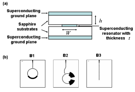
The measurement results presented in this paper belong to three nonlinear NbN superconducting microwave resonators. The resonators were fabricated using stripline geometry, consisting of two superconducting ground planes, two sapphire substrates, and a center strip deposited in the middle (the deposition was done on one of the sapphire substrates). Fig. 1 shows a schematic diagram illustrating stripline geometry and a top view of the three resonator-layouts. We will refer to the three resonators in the text by the names B1, B2 and B3 as defined in Fig. 1. The sapphire substrates dimensions used were X X whereas the coupling gap between the resonators and their feedline was set to in B1 and B3 and in B2 resonator. The resonators were dc-magnetron sputtered in a mixed Ar/N2 atmosphere, near room temperature. The patterning was done using standard UV photolithography process, whereas the NbN etching was performed by Ar ion-milling. The sputtering parameters, fabrication details, design considerations as well as physical properties of the NbN films can be found elsewhere nonlinear features BB . The critical temperature of B1, B2 and B3 resonators were relatively low and equal to and respectively. The thickness of the NbN resonators were Å in B1, Å in B2, and Å in B3 resonator.
III NONLINEAR RESONANCE RESPONSE
In the following subsections, we present experimental results emphasizing the different aspects of the nonlinear response exhibited by B1, B2 and B3 resonators. In subsection A, a resonance response measurement obtained while varying the input rf power is presented, showing an abrupt and low power onset of nonlinearity. In subsections B, C and D, representative experimental results measured while scanning the resonance response in the forward and backward directions are shown, exhibiting respectively, hysteresis loops changing direction, metastability and multiple jumps. Whereas in subsection E, the dependence of the resonance lineshape on applied dc magnetic field is examined, showing a change in the direction of the jump and a jump vanishing features. All measurements presented were performed at liquid helium temperature , and the results were verified using two configurations, immersing in liquid helium and in vacuum.
III.1 Abrupt onset of nonlinearity
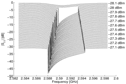
In Fig. 2 we present a parameter measurement of B1 first mode using a vector network analyzer. At low input powers, the resonance response lineshape is Lorentzian and symmetrical. As the input power is increased gradually in steps of dBm, the resonance response changes dramatically and abruptly at about dBm. It becomes extremely asymmetrical, and includes two abrupt jumps at both sides of the resonance lineshape. The magnitude of the jumps at some input powers, can be as high as dB. As the input power is increased the resonance frequency is red shifted and the jump frequencies shift outwards away from the center frequency. Moreover at much higher powers not shown in the figure, the resonance curve becomes gradually shallower and broader in the frequency span. It is also worthwhile noting that the intensive evolution of the resonance lineshape shown in Fig. 2 takes place within only dBm power range.
III.2 Hysteretic behavior
As the equation of motion for nonlinear systems becomes multiple valued or lacks a steady state solution in some parameter domain, nonlinear systems tend to demonstrate hysteretic behavior with respect to that parameter.
Frequency hysteresis in the resonance lineshape of superconducting resonators exhibiting Duffing oscillator nonlinearity and other kinds of nonlinearities were observed by several groups HTS patch antenna ; Nonlinear TL . Hysteretic behavior and losses in superconductors were discussed also in Refs. vortices ; vortex dynamics . Moreover recent works, which examined the resonance response of rf tank circuit coupled to a SQUID, have reported several interesting frequency hysteresis features opposed hammerhead ; Pinch resonances in rf ; nonlinear multilevel .
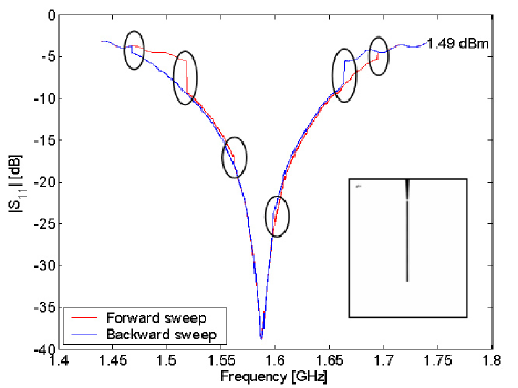
Likewise measuring the resonance response of our nonlinear resonators yields a hysteretic behavior in the vicinity of the jumps. However, this hysteretic behavior is unique in many aspects. In Fig. 3 we show a measurement of B1 resonator at its first mode, measured while sweeping the frequency in both directions. The input power range shown in this measurement corresponds to a higher power range than that of Fig. 2. The red line represents a forward frequency sweep, whereas the blue line represents a backward frequency sweep.
At dBm the resonance lineshape contains two jumps in each scan direction and two hysteresis loops. The left hysteresis loop circulates clockwise whereas the right loop circulates counter clockwise. However the common property characterizing them is that the jumps occur at higher frequencies in the forward scan compared to their counterparts in the backward scan. As the input power is increased to about dBm the two opposed jumps at the left side meet and the left hysteresis loop vanishes. At about dBm a similar effect happens to the right hysteresis loop, and it vanishes as well. Whereas at higher input powers (i.e. dBm, dBm) the two jumps occur earlier at each frequency sweep direction, causing the hysteresis loops to appear circulating in the opposite direction compared to the dBm resonance curve for instance. As we show in the next subsection, this picture of well defined hysteresis loops is strongly dependent on the applied frequency sweep rate and on the system noise. A possible explanation for this unique hysteretic behavior would be presented in Sec. VI.

III.3 Metastable states
Jumps in the resonance response of a nonlinear oscillator are usually described in terms of metastable/stable states and dynamic transition between basins of attraction of the oscillator Cleland , thus in order to examine the stability of these observed resonance jumps, we carried out several measurements.
In one measurement, we have ”zoomed in” around the right jump of the resonance at dBm and examined its frequency response in both directions. The measurement setup included a signal generator, the cooled resonator and a spectrum analyzer. The reflected signal power off the resonator was redirected by a circulator, and measured using a spectrum analyzer. The measurement result obtained using sampling points in each direction, is exhibited in the inset of Fig. 3, where the metastable nature of the jump region is clearly demonstrated.
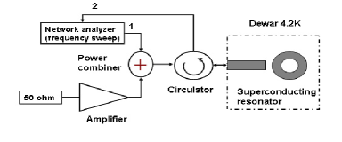
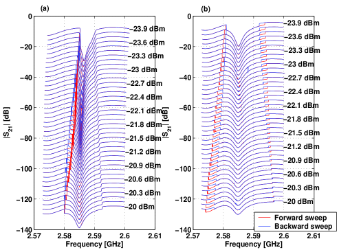
In another measurement configuration we have investigated this metastability further by monitoring the effect of applied broadband noise on the resonance jumps. We applied a constant white noise power to the resonator, several orders of magnitude lower than the main signal power, using the setup depicted in Fig. 4. The applied white noise level was dBm/Hz (measured separately using spectrum analyzer), and was generated by amplifying the thermal noise of a room temperature load using an amplifying stage. The generated noise was added to the transmitted power of a network analyzer via a power combiner. The power reflections were redirected by a circulator, and were measured at the second port of the network analyzer. The effect of the dBm/Hz white noise power on B1 first mode jumps, is shown in Fig. 5 (a), whereas in Fig. 5 (b) we show for comparison the nearly noiseless case obtained after disconnecting the amplifier and the combiner stage. The two measurements were carried out in the same input power range ( dBm through dBm).
By comparing between the two measurement results, one can make the following observations. The two fold jumps in Fig. 5 (b) form a hysteresis loop at both sides of the resonance curve. By contrast in Fig. 5 (a), as a result of the added noise, the hysteresis loops at the right side vanish, while the jumps at the left side, become frequent and bidirectional (indicated by the thick colored lines).
At a given input drive, the transition rate between the oscillator basins of attraction, can be generally estimated by the expression Cleland , where is the quasi-activation energy of the oscillator, is proportional to the noise power, is Boltzmann’s constant, is the oscillator frequency, whereas is related to Kramers low-dissipation form Kramer and it is given approximately by , where is the natural resonance frequency, and is the quality factor of the oscillator. From our results we roughly estimate the order of magnitude of to be for the jump on the left Cleland . Note however that this quantity varies between different transitions and strongly depends on the operating point.
III.4 Multiple jumps
Another nonlinear feature, namely multiple jumps in the resonance lineshape, is observed when measuring the resonance response of B3, while sweeping the frequency in the forward and backward directions. In Fig. 6 we show a representative measurement of the first resonance of B3 corresponding to dBm input power, exhibiting three jumps in each sweep direction and four hysteresis loops.
III.5 Dc magnetic field dependence
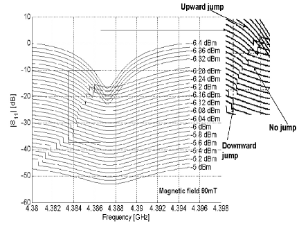
Measuring B2 resonator second mode under dc magnetic field yielded additional nonlinear features in the resonance response lineshape as shown in Figs. 7, 8.
In Fig. 7 we show the resonance lineshape of B2 second mode measured while applying a perpendicular dc magnetic field of . As the input rf power is increased gradually, the resonance lineshape undergoes different phases. While at low and high powers the curves are Lorentzians and symmetrical, in the intermediate range, the resonance curves include a jump at the left side, which, as the input power increases, flips from the upward to the downward direction.
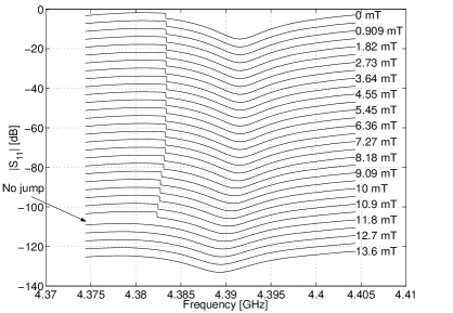
Whereas in Fig. 8, where we have set a constant input power of dBm and increased the applied magnetic field by small steps, the left side jump vanishes as the magnetic field exceeds some relatively low threshold of . These effects will be further discussed in Secs. V and VI.
IV COMPARISON WITH OTHER NONLINEARITIES
The most commonly reported nonlinearity in superconductors is the Duffing oscillator nonlinearity. However this nonlinearity is qualitatively different from the nonlinearity we observe in our NbN samples and which is reported in this paper. In Fig. 9 we show, for the sake of visual comparison, a resonance response measured at , exhibiting Duffing oscillator nonlinearity of the kind generally reported in the literature nonlinear dynamics ; Thermally induced nonlinear behaviour ; RF power dependence CP YBCO . This nonlinearity which can be explained in terms of resistance change and kinetic inductance change Dahm ; Nonlinear TL was measured at the first resonance frequency of a Å thickness Nb resonator employing B2 layout geometry (). The differences between the two nonlinear dynamics shown in Figs. 2 and 9, are obvious. In Fig. 9 the nonlinearity is gradual, while in Fig. 2 the power onset of nonlinearity is abrupt and sudden. In Fig. 9, the resonance response in the nonlinear regime, contains an infinite slope at the left side, whereas in Fig. 2 the curves contain two jumps at both sides of the resonance response. In Fig. 9 changes in the resonance curve are measured on power scale of dBm, while changes in Fig. 2 are measured on dBm scale. Whereas the onset of nonlinearity in Fig. 9 is of the order of dBm, the onset of nonlinearity in Fig. 2 is about orders of magnitudes lower dBm. Furthermore, by taking into account the differences in the hysteretic behavior of the two nonlinearities and the multiple jumps feature shown in Fig. 6, the special characteristics of the reported nonlinearity are further established.
Abrupt jumps in the resonance lineshape similar in some aspects to the jumps reported herein, were observed in two-port high- YBCO resonators HTS patch antenna ; power dependent effects observed for sc stripline resonator ; mw power handling weak links thermal effects . Portes et al. HTS patch antenna have also reported some frequency hysteretic behavior in the vicinity of the jumps. However, one significant difference between the two nonlinearities is the onset power of nonlinearity reported in these references, which is on the order of dBm power dependent effects observed for sc stripline resonator ; mw power handling weak links thermal effects , that is about orders of magnitude higher than the onset power of nonlinearity of B1 first mode ( dBm). All three works HTS patch antenna ; power dependent effects observed for sc stripline resonator ; mw power handling weak links thermal effects have attributed the nonlinear abrupt jumps to local heating of distributed WL in the resonator film.

V POSSIBLE NONLINEAR MECHANISMS
The relatively very low onset power of nonlinearity observed in these resonators as well as its strong sensitivity to rf power, highly imply an extrinsic origin of these effects, and as such, hot spots in WL is a leading candidate for explaining the nonlinearity.
Vortex penetration in the bulk or WL is less likely, mainly because heating the sample above between sequential magnetic field measurements, have yielded reproducible results with a good accuracy in the magnetic field magnitude, the microwave input power and in the jump frequency (less than offset). Moreover the low magnetic field threshold above which the B2 resonance jump vanished, is about times lower than (flux penetration) of NbN reported for example in nonlinear dynamics .
In the following subsection A, we provide a direct evidence of WL. Whereas in subsection B, we exclude global heating mechanism as a possible source of the effects.
V.1 Columnar structure
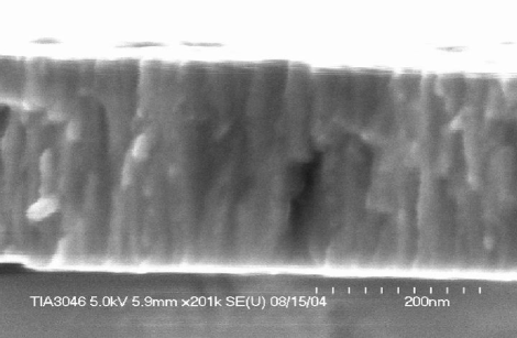
It is well known from numerous research works done in the past rf superconducting properties of reactively sputtered NbN ; superconducting properties and NbN structure , that NbN films can grow in a granular columnar structure under certain deposition conditions. Such columnar structure may even promote the growth of random WL at the grain boundaries of the NbN films. To study the NbN granular structure we have sputtered about NbN film on a thin small rectangular sapphire substrate of thickness. The sputtering conditions applied were similar to those used in the fabrication of B2 resonator. Following the sputtering process, the thin sapphire was cleaved, and a scanning electron microscope (SEM) micrograph was taken at the cleavage plane. The SEM micrograph in Fig. 10 which clearly shows the columnar structure of the deposited NbN film and its grain boundaries, further supports our weak link hypothesis. The typical diameter of each NbN column is about
V.2 Frequency sweep time analysis
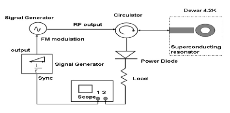
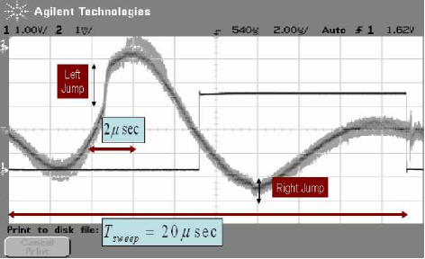
Resistive losses and heating effects are typically characterized by relatively long time scales Thermally induced nonlinear behaviour . In attempt to consider whether such effects are responsible for the observed nonlinearities in general and for the jumps in particular, we have run frequency sweep time analysis using the experimental setup depicted in Fig. 11. We have controlled the frequency sweep cycle of a signal generator via FM modulation. The FM modulation was obtained by feeding the signal generator with a saw tooth waveform having sweep time cycle. The reflected power from the resonator was redirected using a circulator and measured by a power diode and oscilloscope. The left and right hand jumps of B2 resonance were measured using this setup, while applying increasing FM modulation frequencies up to . In Fig. 12 we present a measurement result obtained at FM modulation, or alternatively of . The FM modulation applied was around center frequency. The measured resonance response appears inverted in the figure due to the negative output polarity of the power diode. The fact that both jumps continue to occur within the resonance lineshape (see Fig. 12), in spite of the short duty cycles that are of the order of , indicates that heating processes which have typical time scale on the order of to Thermally induced nonlinear behaviour are unlikely to cause these effects.
However the above measurement result does not exclude local heating of WL Bol ; Nonequilibrium ; Use . Assuming that the substrate is isothermal and that the hot spot is dissipated mainly down into the substrate rather than along the film Bol , one can evaluate the characteristic relaxation time of the hot spot using the equation where is the heat capacity of the superconducting film (per unit volume), is the film thickness, and is the thermal surface conductance between the film and the substrate Nonequilibrium . Substituting for our B2 NbN resonator yields a characteristic relaxation time of where the parameters (NbN) Use , (B2 thickness), and at (sapphire substrate) Use , have been used. Similar calculation based on values given in Ref. Bol yields These time scales are of course 2-3 orders of magnitude lower than the time scales examined by the FM modulation setup, and thus local heating of WL is not ruled out.
VI LOCAL HEATING of WL MODEL
In this section we consider a hypothesis according to which local heating of WL is responsible for the observed effects. We show that this hypothesis can account for the main nonlinear features observed, and that simulations based on such a theoretical model, exhibit a very good qualitative agreement with experimental results.
VI.1 Theoretical modeling
Consider a resonator driven by a weakly coupled feedline carrying an incident coherent tone , where is a constant complex amplitude and is the drive angular frequency. The mode amplitude inside the resonator can be written as , where is a complex amplitude, which is assumed to vary slowly on the time scale of . In this approximation, the equation of motion of reads Yurke
| (1) |
where is the angular resonance frequency, , is the coupling constant between the resonator and the feedline, and is the damping rate of the mode. The term represents input noise with vanishing average
| (2) |
and correlation function given by
| (3) |
In thermal equilibrium and for the case of high temperature , where is Boltzmann’s constant, one has
| (4) |
In terms of the dimensionless time Eq. (1) reads
| (5) |
where
| (6) |
Small noise gives rise to fluctuations around the steady state solution . A straightforward calculation yields
| (7) |
The output signal reflected off the resonator can be written as . The input-output relation relating the output signal to the input signal is given by Gardiner
| (8) |
Whereas the total power dissipated in the resonator can be expressed as Yurke
| (9) |
where .
Furthermore, consider the case where the nonlinearity is originated by a local hot spot in the stripline resonator. If the hot spot is assumed to be sufficiently small, its temperature can be considered homogeneous. The temperature of other parts of the resonator is assumed be equal to that of the coolant . The power heating up the hot spot is given by where .
The heat balance equation reads
| (10) |
where is the thermal heat capacity, is the power of heat transfer to the coolant, and the heat transfer coefficient. Defining the dimensionless temperature hot spots
| (11) |
where is the critical temperature, one has
| (12) |
where
| (13) |
| (14) |
| (15) |
While in Duffing oscillator equation discussed in Ref. Yurke , the nonlinearity can be described in terms of a gradually varying resonance frequency dependent on the amplitude of the oscillations inside the cavity, in the current case, the resonance frequency , the damping rates , and factor are considered to have a step function dependence on , the temperature of the WL
| (16) |
| (17) |
| (18) |
| (19) |
In general, while disregarding noise, the coupled differential equations (5) and (12) may have up to two different steady state solutions. A superconducting steady state of the WL exists when , or alternatively when , where . Similarly, a normal steady state of the WL exists when , or alternatively when , where .
In general, the reflection coefficient in steady state is given by Yurke
| (20) |
VI.2 Simulation results
Simulating the resonator system using this local heating WL model, yields results which qualitatively agree with most of the nonlinear effects previously presented. In subsection (1) we simulate the main effects of Sec. III (A, B, C, D), whereas in subsection (2) we simulate and provide a possible explanation to the nonlinear features of Sec. III (E).
VI.2.1 Abrupt jumps and hysteretic behavior
In Fig. 13 we show a resonance response simulation result based on the hot spot model, which simulates the abrupt jump exhibited in Fig. 2. The solid and dotted lines represent valid steady state solutions of the system and invalid steady state solutions respectively. Whereas the blue and red colors represent superconducting WL solutions and normal WL solutions respectively. In plot (a) the superconducting WL solution is valid in the normalized frequency span, and therefore the system follows this lineshape without jumps. As we increase the amplitude drive we obtain a result seen in plot (b). As the frequency is swept, jumps in the resonance response are expected to take place as the solution followed by the system (according to the initial conditions) becomes invalid. Thus in the forward sweep direction (as the frequency sweep of Fig. 2), we get two jumps indicated by black arrows on the figure. Similar to Fig. 2, the magnitudes of the jumps in the plot are unequal (the left jump is higher). This difference in the magnitude of the jumps is generally dependent on the relative position between the two resonance frequencies (Eq. 16), while in measurement due to the metastability of the system in the hysteretic regime, it depends also on the frequency sweep rate. The simulation parameters used in the different cases are indicated in the figure captions.
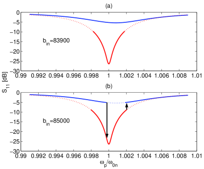
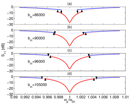
The behavior of the frequency hysteresis loops exhibited in Fig. 3 is simulated in Fig. 14. The different plots exhibited in Fig. 14 correspond to the different cases shown in Fig. 3. In plot (a) the jumps in the forward direction (indicated by the arrows in that direction) occur at higher frequencies than the jumps in the backward direction. Whereas in plot (b) corresponding to a higher amplitude drive we show a case in which the left side hysteresis loop vanish as the two opposed jump frequencies coincide. If we increase further, then at some amplitude drive level as shown in plot (c), we get a similar case of hysteresis loop vanishing at the right side of the resonance response. Whereas at the left side we get a frequency region where both the superconducting and the normal WL solutions are invalid. In this instable region, transitions between the invalid solutions are expected, depending on the number of the sampling points, the sweep time, and the internal noise. However due to this instability, the system is highly expected to jump ”early” in each frequency direction, as it enters this region (at lower frequencies in the forward direction, and at higher frequencies in the backward direction). Thus leading to the observed change in the direction of the hysteresis loop. By increasing further, one obtains a case in which both hysteresis loops are circulating in the opposite direction compared to plot (a).
Furthermore the intermediate jump indicating instability, which appear at the left jump region of the last resonance curve in Fig. 3 (corresponding to dBm), can be explained by this model as well. By solving the coupled Eqs. (5), (12) in the time domain for a single normalized frequency (arbitrarily chosen in the left side hysteresis region) and using the simulation parameters of plot (d) in Fig. 14, one obtains the oscillation pattern of the dimensionless parameter shown in Fig. 15, as a function of the dimensionless time . The oscillations indicating instability are between the superconducting and the normal values, corresponding to and respectively.
As to the multiple jumps feature exhibited in Fig. 6, a straightforward generalization of the model may be needed in order to account for this effect. Such generalization would include WL having a variation in their sizes and critical current along the stripline. Thus causing them to switch to normal state at different current drives (at different frequencies) and as a result induce more than two jumps in the resonance lineshape.
VI.2.2 Magnetic field dependence
In this subsection we show how the model of local heating of WL can also account for the nonlinear dynamics of the resonance lineshape observed under applied magnetic field.
To this end, we show in Fig. 16 a simulation result based on the WL local heating model, which qualitatively regenerates the nonlinear behavior of the resonance lineshape of B2 under a constant magnetic field (presented in Fig. 7). At low drive amplitude , only the superconducting WL steady state solution exists, and thus no jump occurs as one sweeps the frequency (plot (a)). Increasing the drive amplitude (plot (b)) causes the superconducting WL solution to become invalid in the center frequency region, thus the resonance response jumps upward (as the system reaches the invalid region) and stabilizes on the normal WL steady state solution, as indicated by arrows on the plot. By increasing the drive amplitude further (plot (c)) there exists an intersection point where a smooth transition without a jump is expected to occur between the valid superconducting WL solution and the valid normal one. Whereas in plot (d) where we have increased further, a downward jump in the resonance response occurs as the valid normal WL solution lies below the invalid superconducting WL solution. Finally in plot (e) corresponding to a much higher drive, only the normal WL steady state solution exists within the frequency span and therefore there are no jumps in the resultant curve.
Another measurement which can be explained using the WL model, is the measurement shown in Fig. 8, where the left side jump vanishes as the magnetic field increases above some low magnetic field threshold. This result can be explained in the following manner. Increasing the applied dc magnetic field would inevitably increase the screening supercurrent flowing in the film and the local heating of WL. As the local heating exceeds some threshold, the superconducting WL solution would become invalid (for the same frequency span), and consequently the system would only follow the normal WL solution without apparent jumps.
VII SUMMARY
In attempt to investigate and manifest nonlinear effects in superconducting microwave resonators, several superconducting NbN resonators employing different layouts, but similar sputtering conditions have been designed and fabricated. The resonance lineshapes of these NbN resonators having very low onset of nonlinearity, several orders of magnitude lower than other reported nonlinearities nonlinear dynamics ; mw hysteretic losses in YBCO and NbN ; Palomba , exhibit some extraordinary nonlinear dynamics. Among the nonlinearities observed, while applying different measurement configurations, abrupt metastable jumps in the resonance lineshape, hysteresis loops changing direction, multiple jumps, vanishing jumps and jumps changing direction. These effects are hypothesized to originate from weak links located at the boundaries of the columnar structure of the NbN films. This hypothesis is fully consistent with SEM micrographs of these films, and generally agrees with the extrinsic like behavior of these resonators. To account for the various nonlinearities observed, a theoretical model assuming local heating of weak links is suggested. Furthermore, simulation results employing this model are shown to be in a very good qualitative agreement with measurements.
Such strong sensitive nonlinear effects reported herein may be utilized in the future in a variety of applications, ranging from qubit coupling in quantum computation, to signal amplification IMD amplifier and to the demonstration of some important quantum effects in the microwave regime nonlinear coupling ; Yurke .
ACKNOWLEDGEMENTS
E.B. would especially like to thank Michael L. Roukes for supporting the early stage of this research and for many helpful conversations and invaluable suggestions. Very helpful conversations with Oded Gottlieb, Gad Koren, Emil Polturak, and Bernard Yurke are also gratefully acknowledged. This work was supported by the German Israel Foundation under grant 1-2038.1114.07, the Israel Science Foundation under grant 1380021, the Deborah Foundation and Poznanski Foundation.
References
- [1] R. Movshovich, B. Yurke, P. G. Kaminsky, A. D. Smith, A. H. Silver, R. W. Simon, and M. V. Schneider, Phys. Rev. Lett. 65, 1419 (1990).
- [2] B. Yurke, P. G. Kaminsky, R. E. Miller, E. A. Whittaker, A. D. Smith, A. H. Silver, and R. W. Simon, IEEE Trans. Mag. 25, 1371 (1989).
- [3] B. Yurke and E. Buks, quant-ph/0505018.
- [4] E. Buks and B. Yurke, quant-ph/0511033.
- [5] I. Siddiqi, R. Vijay, F. Pierre, C. M. Wilson, M. Metcalfe, C. Riggetti, L. Frunzio, and M. H. Devoret, Phys. Rev. Lett. 93, 207002 (2004).
- [6] I. Siddiqi, R. Vijay, F. Pierre, C. M. Wilson, L. Frunzio, M. Metcalfe, C. Riggetti, R. J. Schoelkopf, M. H. Devoret, D. Vion and D. Esteve, Phys. Rev. Lett. 94, 027005 (2005).
- [7] P. J. Burke, R. J. Schoelkopf, D. E. Prober, A. Skalare, B. S. Karasik, M. C. Gaidis, W. R. McGrath, B. Bumble, and H. G. LeDuc, J. Appl. Phys. 85, 1644 (1999).
- [8] R. Sobolewski, A. Verevkin, G. N. Gol’tsman, A. Lipatov and K. Wilsher, IEEE Trans. Appl. Supercond. 13, 1151 (2003).
- [9] I. Chiorescu, Y. Nakamura, C. J. P. M. Harmans, and J. E. Mooij, Science 299, 1869 (2003).
- [10] T. Dahm and D. J. Scalapino, J. Appl. Phys. 81, 2002 (1997).
- [11] Z. Ma, E. de Obaldia, G. Hampel, P. Polakos, P. Mankiewich, B. Batlogg, W. Prusseit, H. Kinder, A. Anderson, D. E. Oates, R. Ono, and J. Beall, IEEE trans. Appl. Supercond. 7, 1911 (1997).
- [12] R. B. Hammond, E. R. Soares, B. A. Willemsen, T. Dahm, D. J. Scalapino, and J. R. Schrieffer, J. Appl. Phys. 84, 5662 (1998).
- [13] C. C. Chen, D. E. Oates, G. Dresselhaus and M. S. Dresselhaus, Phys. Rev. B. 45, 4788 (1992).
- [14] L. F. Cohen, A. L. Cowie, A. Purnell, N. A. Lindop, S. Thiess, and J. C. Gallop, Supercond. Sci. and Technol. 15, 559 (2002).
- [15] A. L. Karuzskii, A. E. Krapivka, A. N. Lykov, A. V. Perestoronin, and A. I. Golovashkin, Physica B 329-333, 1514 (2003).
- [16] Z. Ma, E. D. Obaldia, G. Hampel, P. Polakos, P. Mankiewich, B. Batlogg, W. Prusseit, H. Kinder, A. Anderson, D. E. Oates, R. Ono, and J. Beall, IEEE Trans. Appl. Supercond. 7, 1911 (1997).
- [17] J. Wosik, L.-M. Xie, J. H. Miller, Jr., S. A. Long, and K. Nesteruk, IEEE Trans. Appl. Supercond. 7, 1470 (1997).
- [18] B. A. Willemsen, J. S. Derov, J. H. Silva, S. Sridhar, IEEE Trans. Appl. Supercond. 5, 1753 (1995).
- [19] A. M. Portis, H. Chaloupka, M. Jeck, and A. Pischke, Superconduct. Sci. & Technol. 4, 436 (1991).
- [20] S. J. Hedges, M. J. Adams, and B. F. Nicholson, Elect. Lett. 26, 977 (1990).
- [21] J. Wosik, L.-M. Xie, R. Grabovickic, T. Hogan, and S. A. Long, IEEE Trans Appl. Supercond. 9, 2456 (1999).
- [22] D.E. Oates, M. A. Hein, P. J. Hirst, R. G. Humphreys, G. Koren, and E. Polturak, Physica C. 372-376, 462 (2002).
- [23] M. A. Golosovsky, H. J. Snortland, and M. R. Beasley, Phys. Rev. B. 51, 6462 (1995).
- [24] S. K. Yip and J. A. Sauls, Phys. Rev. lett. 69, 2264 (1992).
- [25] D. E. Oates, H. Xin, G. Dresselhaus, and M. S. Dresselhaus, IEEE Trans. Appl. Supercond. 11, 2804 (2001).
- [26] B. B. Jin and R. X. Wu, J. of Supercond. 11, 291 (1998).
- [27] A. V. Velichko, D. W. Huish, M. J. Lancaster, and A. Porch, IEEE Trans. Appl. Supercond. 13, 3598 (2003).
- [28] J. Halbritter, J. Appl. Phys. 68, 6315 (1990).
- [29] B. Abdo, E. Segev, Oleg Shtempluck, and E. Buks, IEEE Trans. Appl. Supercond. (to be published), cond-mat/0501114.
- [30] J. H. Oates, R. T. Shin, D. E. Oates, M. J. Tsuk, and P. P. Nguyen, IEEE Trans. Appl. Supercond. 3, 17 (1993).
- [31] H. Xin, D.E. Oates, G. Dresselhaus, and M. S. Dresselhaus, J. Supercond. 14, 637 (2001).
- [32] R. Whiteman, J. Diggins, V. Schöllmann, T. D. Clark, R. J. Prance, H. Prance, and J. F. Ralph, Phys. Lett. A 234, 205 (1997).
- [33] H. Prance, T. D. Clark, R. Whiteman, R. J. Prance, M. Everitt, P. Stiffel, and J. F. Ralph, cond-mat/0411139.
- [34] R. J. Prance, R. Whiteman, T. D. Clark, H. Prance, V. Schöllmann, J. F. Ralph, S. Al-Khawaja, and M. Everitt, Phys. Rev. Lett. 82, 5401 (1999).
- [35] J. S. Aldridge and A. N. Cleland, cond-mat/0406528.
- [36] H. A. Kramers, Physica 7, 284 (1940).
- [37] D. M. Sheen, S. M. Ali, D. E. Oates, R. S. Withers, and J. A. Kong, IEEE Trans. Appl. Supercond. 1, 108 (1991).
- [38] M. W. Johnson, A. M. Herr, and A. M. Kadin, J. Appl. Phys. 79, 7069 (1996).
- [39] A. M. Kadin and M. W. Johnson, Appl. Phys. Lett. 69, 3938 (1996).
- [40] K. Weiser, U. Strom, S. A. Wolf, and D. U. Gubser, J. Appl. Phys. 52, 4888 (1981).
- [41] S. Isagawa, J. Appl. Phys. 52, 921 (1980).
- [42] Y. M. Shy, L. E. Toth, and R. Somasundaram, J. Appl. Phys. 44, 5539 (1973).
- [43] C. W. Gardinar and M. J. Collett, Phys. Rev. A 31, 3761 (1985).
- [44] A. VI. Gurevich and R. G. Mints, Rev. Mod. Phys. 59, 941 (1987).
- [45] P. P. Nguyen, D. E. Oates, G. Dresselhaus, M. S. Dresselhaus, and A. C. Anderson, Phys. Rev. B 51, 6686 (1995).
- [46] A. Andreone, A. Cassinese, A. Di Chiara, M. Lavarone, F. Palomba, A. Ruosi, and R. Vaglio, J. Appl. Phys. 82, 1736 (1997).
- [47] B. Abdo, E. Segev, O. Shtempluck, and E. Buks, cond-mat/0507056.
- [48] B. Abdo, E. Segev, O. Shtempluck, and E. Buks, cond-mat/0501236.