Phenomenology of the 0.7 conductance feature
Abstract
We describe a phenomenological model for the conductance feature near that occurs in quantum point contacts. We focus on the transconductance at finite source-drain bias and contrast our model with the results expected from a single-particle picture. Good agreement is seen in comparing the model with experimental data, taken on ultra-low-disorder GaAs induced electron systems. Although simple, our phenomenology suggests important boundary conditions for an underlying microscopic theory.
keywords:
0.7 , QPC , phenomenological , quantum wire , conductance1 Introduction
The conductance of a quantum point contact (QPC), formed via geometric or electrostatic confinement of a two-dimensional electron system (2DES), is quantized in units of [1, 2]. This quintessentially quantum-mechanical phenomena is well explained in terms of the single-particle discrete energy spectrum associated with the confining potential [3]. QPCs also exhibit unexpected non-quantized features that cannot be explained within this non-interacting, single-particle picture. A clear example is the feature occurring below the first conductance plateau, in the range and at equivalent positions for higher plateaus. This anomalous conductance structure was observed in the earliest transport measurements on ballistic QPCs [1, 2] but has remained largely unexplained despite numerous experimental investigations [4, 5, 6, 7, 8, 9, 10, 11, 12, 13, 14, 15, 16, 17, 18, 19] and is regarded as a key outstanding problem in mesoscopic physics [20].
A prime result, initially uncovered by Thomas et al., [4] is the evolution of the with increasing parallel magnetic field into the well understood Zeeman spin-split plateau at . This observation strongly suggests that the structure at is related to a many-body state in which symmetry is broken between spin-up and spin-down electrons.
2 Phenomenological model
Here we describe a simple phenomenological model that is in striking agreement with the experimental behavior of the conductance feature with temperature , magnetic field , source-drain bias and potential profile. At the core of this model is the conjecture that a density-dependent spin-gap opens in the one-dimensional (1D) energy spectrum as the gate voltage is made less negative [13, 21]. Fig. 1a captures the essence of the model. Before the first 1D sub-band is occupied (below energy in Fig. 1a) the spin-up and spin-down sub-bands are degenerate. As the 1D states begin to fill the spin-down band rapidly moves down in energy with the available spin-up states moving higher in energy above the Fermi-level (). The model assumes a parabolic dependence of the Fermi-energy on gate voltage () in connection with the usual form of the 1D density of states [22]. For a detailed discussion of this model we refer the reader to Refs. [21, 16].
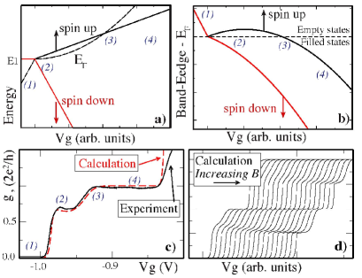
Features in conductance are related to the occupation probability of the 1D sub-bands and are a function of temperature and the energy difference between the sub-band edge and . Within the context of our model, Fig. 1b shows the difference between the spin-dependent band-edge energy and as a function of gate voltage . It is the functional form of this difference between the spin band-edges and that relates to the experimental data (since it sets the conductance) and of prime importance in suggesting possible ‘boundary conditions’ of an underlying microscopic theory. We point out that in contrast to a similar model based on pinning of the band-edge [23], in our picture the spin-down energy continues to move rapidly below the Fermi-level as the gate voltage is swept.
Figure 1c (taken from Ref [21]) compares differential conductance calculations based on this model with data taken on an ultra-low-disorder quantum wire at =50mK (See Refs [13, 16, 21] for experimental details). We take the simplest approximation and calculate conductance with a step transmission function in the limit of zero source-drain bias. Importantly, the only free-parameter needed to fit the model to the experimental data is the rate at which the spin-gap opens with gate voltage [21]. Note the small discrepancy between model and experiment at the top right of Fig. 1c which is due to the step transmission function (no tunneling) that is used in the calculation rather than a more realistic smoothly varying [3]. Fig. 1d (also taken from Ref. [21]) shows conductance calculations as a function of increasing parallel magnetic field, in which a smooth evolution of the conductance feature from to is observed, consistent with the experimental results [4, 15, 24].
3 Single-particle results
We now focus on the transconductance () at finite which facilitates the study of transitions between the conductance plateaus as a function of chemical potential or gate voltage . We firstly compare transconductance plots based on our model to the single-particle case at zero and finite magnetic field. Fig. 2a shows a transconductance intensity plot as a function of and calculated using the usual single-particle formalism [25, 26]. We assume the conductance at finite bias is approximated by the weighted average of two zero conductances, one for the chemical potential of the source () and the other for the drain (), where characterizes the symmetry of the potential drop across the constriction [26]. Centered about =0 are the linear response integer-plateau diamonds (dark) at and . Symmetric either side of the integer plateaus are the finite bias ‘half-plateaus’ that occur when the chemical potential of the source () or drain () differ by one (spin degenerate) sub-band ( and ) [27].
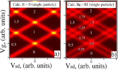
With the application of an in-plane magnetic field the spin degeneracy is lifted and additional Zeeman spin-split plateaus appear at at =0 as shown in Fig. 2b. At finite bias and high magnetic field new plateaus also appear at . These are the finite bias ‘half-plateaus’ that now occur at quarter intervals with the lifting of the spin degeneracy. The relative size of these ‘quarter-plateaus’ in comparison to the half-plateaus simply depends on the relative Zeeman splitting to sub-band energy spacing. In Fig. 2b we show calculations for =8T, setting the in-plane -factor to the bulk value of 0.44.
4 Comparison of model with experiment
Returning to our phenomenology, Fig. 3a shows transconductance calculations based on the model. At low gate voltage the sub-bands are spin-degenerate and the transconductance looks similar to the =0 single-particle case of Fig. 2a (in the range ). With increasing 1D density (making the gate voltage less negative) the degeneracy begins to lift as a spin-gap opens in the 1D energy spectrum. At the transconductance now resembles Fig. 2b as the spin degeneracy is lifted and finite-bias plateaus beginning at are observed.
Figure 3b shows data taken on an ultra-low-disorder quantum wire at =100mK. In these devices the electrons in both the 1D and 2D regions are induced via the application of positive bias to a surface gate [6]. Close examination of the experimental data reveals an absence of finite bias plateaus at and the presence of features, resembling our calculated results in Fig. 3a. This behavior is consistent with a picture of a density-dependent spin gap opening with gate voltage.
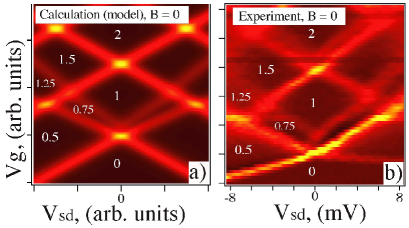
Of particular interest is the occurrence of weak features at , beyond the needed to produce the usual half-plateaus. These weak structures, which are present in both our calculations and experimental data, connect to the usual feature via the line that intersects the top half of the first () diamond (either side of the label ‘1’). In the context of the model these high features arise from the chemical potential of the source and drain differing by 3 spin sub-bands, as in the case where the source is at (above 4 spin band-edges) and the drain is at (in the gap between the first spin-up and spin-down sub-bands). The presence of high bias features provides further evidence that a spin dependent energy gap remains open well below the Fermi-level, continuing to increase (slightly) as the 1D density grows and higher sub-bands are populated.
5 0.7 analogs
We now discuss our phenomenological model in the context of a recent experiment by Graham et al., [24], in which the sub-band energies can be made to cross at very high in-plane magnetic fields. In addition to the usual evolution of the feature towards , Graham et al., discovered the appearance of similar conductance structure at high evolving from into the plateau at . This feature is termed a ‘-analog’. In Fig. 4 we show transconductance calculations based on our model as a function of increasing Zeeman energy (bottom to top). For simplicity we ignore any changes in the electron -factor related to correlation or diamagnetic effects, taking the bulk value of 0.44. This likely accounts for the larger magnetic fields required in our model to achieve sub-band crossing in comparison to experimental observation.
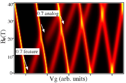
Consistent with the experimental results of Graham et al., [24] we observe the usual feature at =0, indicated in Fig. 4 by the black region separating the spin-up and spin-down transconductance lines that evolve away from each other as is increased. Without adding any new parameters to our model we also find good agreement with the experimental results at magnetic fields where the =1 spin-up sub-band crosses the =2 spin-down sub-band. As in the case of the structure at =0, our model assumes that at high as each spin-band is populated, the Fermi energy is proportional to and the gate-dependent spin gap (intrinsic) adds to the (extrinsic) Zeeman energy of the -field.
Following the crossing of sub-bands there is a discontinuous shift in from the crossing point, marking the appearance of the analog [24]. Our calculations also account for the appearance of higher order analogs at the crossings of =2 spin-up with =3 spin-down sub-bands. The temperature dependence of the analogs follows the usual activated behavior of the feature in our model (not shown). Very recent numerical work [28] using spin-density functional theory also shows good agreement with the experimental results of Graham et al.. How the functional form of our phenomenology relates to these more detailed calculations is an interesting question for future work.
The strong agreement between the transconductance calculations and the experimental data of Graham et al., provide further evidence that this model captures the essence of the functional form underlying the 0.7 feature. Despite this agreement however, the observation of a zero bias anomaly in the bias spectroscopy and the low temperature restoration of the conductance as observed by Cronenwett et al., [15] cannot be explained without extending this model to also include Kondo spin screening in the regime , where is the Kondo temperature. Perhaps a complete explanation will account for a density-dependent gap that is screened by the formation of a Kondo-like state at low temperatures and bias.
6 Conclusions
We have described a simple phenomenological model for the conductance feature that occurs in quantum point contacts. Our focus has been on the transconductance at finite source-drain bias which emphasizes transitions between the conductance plateaus. The calculated results based on our model agree well with data taken on both ultra-low-disorder induced devices and more traditional split-gated heterostructures. Without the inclusion of additional parameters this model also accounts for the observation of analogs at high magnetic field. Although largely empirical, we believe the functional form underlying this simple picture may prove useful in uncovering a detailed microscopic theory of this effect.
7 Acknowledgments
The authors wish to thank C. M. Marcus, T. M. Buehler, D. T. McClure, J. L. O’Brien, S. Das Sarma, K.-F. Berggren, M. J. Biercuk, R. G. Clark, A. Dzurak and A. R. Hamilton for useful discussions. D.J.R. is indebted to L. N. Pfeiffer and K. W. West for the excellent heterostructure material used in the experiments.
References
- [1] B. J. van Wees et al. Phys. Rev. Lett., 60:848, 1988.
- [2] D. A. Wharam et al. J. Phys. C, 21:L209, 1988.
- [3] M. Büttiker. Phys. Rev. B, 41:7906, 1990.
- [4] K. J. Thomas et al. Phys. Rev. Lett., 77:135, 1996.
- [5] K. J. Thomas et al. Phys. Rev. B, 58:4846, 1998.
- [6] B. E. Kane et al. Appl. Phys. Lett., 72:3506, 1998.
- [7] A. Kristensen et al. Physica B, 249:180, 1998.
- [8] A. Kristensen et al. Phys. Rev. B, 62:10950, 2000.
- [9] S. Nuttinck et al. Jpn. J. Appl. Phys., 39:L655, 2000.
- [10] K. J. Thomas et al. Phys. Rev. B., 61:R13365, 2000.
- [11] C.-T. Liang et al. Phys. Rev. B, 60, 1999.
- [12] K. S. Pyshkin et al. Phys. Rev. B., 62:15842, 2000.
- [13] D. J. Reilly et al. Phys. Rev. B, 63:R121311, 2001.
- [14] N. J. Appleyard et al. Phys. Rev. B, 62:R16275, 2000.
- [15] S. M. Cronenwett et al. Phys. Rev. Lett., 88:226805, 2002.
- [16] D. J. Reilly et al. Phys. Rev. Lett., 89:246801, 2002.
- [17] Jonathan. P. Bird and Yuichi Ochiai. Science, 303:1621, 2004.
- [18] P. Roche et al. Phys. Rev. Lett., 93:116602, 2004.
- [19] R. de Picciotto et al. Phys. Rev. Lett., 92:036805, 2004.
- [20] R. Fitzgerald. Phys. Today, 55(5):21, 2002.
- [21] D. J. Reilly. Phys. Rev. B, 72:033309, 2005.
- [22] K. Hirose and N. S. Wingreen. Phys. Rev. B, 64:073305, 2001.
- [23] A. Kristensen and H. Bruus. Physica Scripta: Proc. 19th Nordic Semiconductor Meeting, 2001, 2002.
- [24] A. C. Graham et al. Phys. Rev. Lett., 91:136404, 2003.
- [25] L. I. Glazman and A. V. Khaetskii. Europhys. Lett., 9:263, 1989.
- [26] L. Martín-Moreno et al. J. Phys. C, 4:1323, 1992.
- [27] N. K. Patel et al. Phys. Rev. B, 44:R10973, 1991.
- [28] Karl-Fredrik Berggren, Peter Jaksch, and Irina Yakimenko. Phys. Rev. B, 71:115303, 2005.