Extrinsic photonic crystals
Abstract
Doped semiconductors are intrinsically homogeneous media. However, by applying an external magnetic field that has a spatially periodic variation, doped semiconductors can behave extrinsically like conventional photonic crystals. We show this possibility theoretically by calculating the photonic band structures of a doped semiconductor under an external, spatially periodic magnetic field. Homogeneous media, behaving like conventional photonic crystals under some external, spatially periodic fields, define a new kind of photonic crystals: extrinsic photonic crystals. The proposed extrinsic photonic crystals could not only extend the concept of photonic crystals but also lead to the control of the dispersion and propagation of electromagnetic waves in a unique way: simply manipulating the externally applied fields.
pacs:
42.70.Qs, 78.20.Ls, 78.66.-wIn the areas of computing and communication there has been a strong desire to replace electronic devices with photonic ones due to the fact that as information carriers electromagnetic waves are advantageous in many ways over electrons. One of the promising approaches is based on photonic crystals (PCs).yab:87 ; joh:87 PCs proposed up to now are composite materials with a permittivity or/and a permeability which is a periodic function of the position.joa:95 As a result of the multiple Bragg scatterings, PCs are characterized by complicated photonic band structures. Between photonic bands there may exist photonic band gaps (PBGs), for frequencies within which the propagation of electromagnetic waves is absolutely forbidden. The existence of the complicated photonic band structures and PBGs in PCs allows the control of dispersion and propagation of electromagnetic waves somewhat in a desired way, which can lead to many novel applications.sou:96 ; sak:01 ; ino:04 ; lou:05
In conventional PCs the spatially periodic variation of the permittivity or/and the permeability is obtained by the periodic arrangement of two or more materials. To obtain more degrees of tunability, tunable PCs have been proposed. The tunability relies on the modification of the permittivity or/and the permeability of the constituent materials by some external parameters such as temperature, external electric or magnetic fields.fig:98 ; bus:99 ; kee:00 ; leo:00 ; hal:00 ; kee:01 ; li:03 ; jia:03 ; xu:03 ; tian:05 Tunable PCs proposed up to now still consist of two or more materials. Based on tunable PCs, it is possible to design and fabricate new kinds of optoelectronic and microwave devices such as optical modulators, switches, tunable filters, and tunable resonators.
In the present work we propose and conceptualize a new kind of tunable PCs: extrinsic PCs. Unlike conventional PCs, an extrinsic PC is composed of a single homogenous material, whose permittivity or/and permeability can be altered by applying some external fields. If the applied external filed is spatially periodic, a spatially periodic variation of the permittivity or/and the permeability can be obtained likewise. Consequently, this homogenous material behaves like conventional PCs. Extrinsic PCs may extend the concept of PCs, leading likely to some new applications. To exemplify the idea of extrinsic PCs, we present theoretical calculations of the photonic band structures for a doped semiconductor under a spatially periodic magnetic field. Our results indicate that this doped semiconductor behaves extrinsically like a conventional PC.
In previous worksjia:03 ; xu:03 ; tian:05 we showed that PCs consisting of doped semiconductors can be made tunable under an external magnetic field. The central idea relies on the fact that the dielectric constant of doped semiconductors can be altered by applying an external magnetic field owing to magneto-optical effects.per:67 ; pid:80 In the present work, we take advantage of one of the famous magneto-optical effects, Voigt effect,per:67 ; pid:80 in order to achieve extrinsic PCs. The proposed extrinsic PCs here are composed of a single -doped semiconductor. For frequencies well below the phonon resonance frequency, the dielectric constant of -doped semiconductors is given, in the absence of the external magnetic field, bykit:76
| (1) |
where is the static dielectric constant. The plasma frequency is obtained from
| (2) |
where is the density of electrons, is the effective charge of electrons, and is the effective mass of electrons. In Voigt configuration,per:67 ; pid:80 the propagation direction of electromagnetic waves is perpendicular to the applied magnetic field. The modification of the dielectric constant due to the external magnetic field is different for different polarizations. For -polarization (with the electric field parallel to the external magnetic filed), the dielectric constant is not affected by the applied magnetic field, still given by Eq. (1). For -polarization (with the electric field perpendicular to the external magnetic field), however, the dielectric constant is modified in the presence of the external magnetic field, given bypid:80
| (3) |
The cyclotron frequency is , where is the amplitude of the external magnetic field and is the speed of light in vacuum. It should be noted that for frequencies substantially above the phonon resonance, in Eqs. (1) and (3) should be replaced by the optical dielectric constant . It is obvious that for -polarization the dielectric constant is a function of the external magnetic field . Thus, a spatially periodic variation of the refractive index can be achieved provided that the applied external magnetic field is spatially periodic.

We now consider an external magnetic field that has one-dimensional (1D) and 2D spatially periodic variations as shown schematically in Fig. 1. As a first approximation, it is assumed that the magnitude of the magnetic field is homogeneous everywhere in the applied region, while it is zero outside the applied region. In real cases, the applied magnetic field is not so ideal as assumed, which may lead to some quantitative changes in our results. But it does not affect our conclusions. Under the spatially periodic magnetic field, a doped semiconductor should behave like a conventional PC. Without loss of generality, the doped semiconductor is assumed to be -doped GaAs. The static dielectric constant of GaAs is , taken from Ref. kit:76, .
With a 1D spatially periodic magnetic field applied to -doped GaAs as shown in Fig. 1(a), -doped GaAs behaves like a 1D PC, whose photonic band structures for -polarization as a function of the magnitude of the applied magnetic field are shown in Fig. 2. The photonic band structures are calculated from a transfer matrix method.yeh:88 ; zi:98 In photonic band structure calculations, the lattice constant of the periodic magnetic field is mm and the fraction of the applied region with respect to one unit cell is .
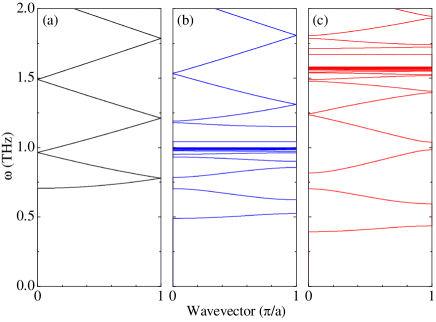
For -polarization, the photonic band structures are not affected by the applied magnetic field, which are exactly the same as those of -polarization in the absence of the magnetic field. There exists a low-frequency band gap that extends up to the plasma frequency . Above , the photonic band structure is simply a folded version from the corresponding dispersion of -doped GaAs. With the applied magnetic field, drastic changes in the photonic band structures for -polarization occur. The upper edge of the low-frequency band gap shifts downwards with the increasing magnetic field. Below , additional photonic bands and PBGs appear. Above , some PBGs open up owing to the multiple Bragg scatterings. Just below , there exist very dense, flat photonic bands owing to the fact that the region applied with the magnetic field has a very large positive dielectric constant. For frequency well above , photonic band structures are less affected due to the fact that the dielectric constant is weakly modified at high frequencies.
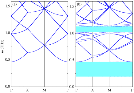
When a 2D spatially periodic magnetic field is applied to -doped GaAs as shown in Fig. 1(b), this -doped GaAs should behave like a 2D PC. The lattice type of the periodically applied magnetic field is square with a lattice constant of mm. The applied regions have circular shapes with a radius of . A plane-wave-based transfer matrix methodli:03b is used to calculate the photonic band structures, shown in Fig. 3. Without the external magnetic field, the photonic band structures for - and -polarizations are degenerate. A band gap exists at the frequencies below and there are no PBGs above . The photonic band structures are a simple folding from the dispersion of -doped GaAs. When a spatially periodic magnetic field is applied, some changes occur in the photonic band structures for -polarization. Unlike in 1D systems, no complete PBGs open up, owing to the fact that the modification by the applied magnetic field is not strong enough to give rise to a strong contrast of the refractive index. However, some additional photonic bands and partial PBGs appear. For example, at Tesla there exists a partial PBG ranging from 0.555 to 0.587 THz along the direction. Similar to the 2D PC composed of a doped semiconductor perforated with air hole arrays,xu:03 some very dense, flat photonic bands are present in two frequency ranges, one from 1.052 to 1.137 THz and other one from 0.195 to 0.471 THz. The existence of the dense, flat photonic bands (shaded regions) is due to fact that the dielectric constant of one of the regions applied with and without the magnetic field is negative, while the dielectric constant in other region is positive. The low-frequency PBG still exists for frequencies below 0.195 THz, where the dielectric constants of the two regions are both negative. For frequencies well above , the photonic band structures are weakly affected as expected.
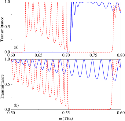
From the above discussions, we show the possibility to achieve extrinsic PCs based on a single -doped semiconductor. It is know that the plasma frequencies of -doped semiconductors lie in the THz regime for reasonable doping densities. Therefore, the proposed GaAs-based extrinsic PCs may have some potential applications in the THz technology such as switches, modulators, tunable filters and resonators. As an example, we show in Fig. 4 the switching effects of finite -doped GaAs under 1D or 2D spatially periodic magnetic filed. For the 1D case, for wavelengths in the vicinity of 0.75 THz, electromagnetic waves can transmit in the absence of the applied magnetic filed. When the magnetic filed is applied, there is no transmission due to the existence of a PBG. For wavelengths in the vicinity of 0.66 THz, there is transmission when the magnetic field is applied, while electromagnetic waves cannot transmit when the magnetic filed is switched off. Similarly, this switching occurs also in the 2D system.
It should be pointed out that point and line defects can be also introduced in extrinsic PCs. This can be achieved by introducing point and line defects in the external, spatially periodic magnetic field. Consequently, tunable cavity and waveguides could be obtained. In the above discussions, the external magnetic field is static. However, the applied magnetic field can be also alternative. As a result, a dynamic control of the optical properties of extrinsic PCs can be achieved, which may lead to some novel applications.
In summary, we proposed and conceptualized a new kind of tunable PCs: extrinsic PCs. Without externally applied fields, they are homogeneous media; when external fields are applied, they are PCs simultaneously. We showed by numerical calculations that a -doped GaAs behaves like conventional PCs under a spatially periodic magnetic field. Our conceptualized extrinsic PC may greatly extend the concept of PCs. Moreover, by manipulating the externally applied fields extrinsic PCs provide with a unique way to control the dispersion and propagation of electromagnetic waves.
This work was mostly supported by CNKBRSF. Partial support from NSFC, PCSIRT, and Shanghai Science and Technology Commission is also acknowledged. One of the authors (J.Z.) thanks Prof. Yanfeng Chen for interesting discussions.
References
- (1) E. Yablonovitch, Phys. Rev. Lett. 58, 2059 (1987).
- (2) S. John, Phys. Rev. Lett. 58, 2486 (1987).
- (3) J. D. Joannopoulos, R. D. Meade, and J. N. Winn, Photonic Crystals (Princeston Univ. Press, Princeton, 1995).
- (4) Photonic Band Gap Materials, edited by C. M. Soukoulis (Kluwer, Dordrecht, 1996).
- (5) K. Sakoda, Optical Properties of Photonic Crystals (Springer, Berlin, 2001).
- (6) Photonic Crystals: Physics, Fabrication and Applications, Springer Series in Optical Sciences, Vol. 94, edited by K. Inoue and K. Ohtaka (Springer, New York, 2004).
- (7) J.-M. Lourtioz, et al., Photonic Crystals: Towards Nanoscale Photonic Devices (Springer, Berlin, 2005).
- (8) A. Figotin, Y. A. Godin, and I. Vitebsky, Phys. Rev. B 57, 2841(1998).
- (9) K. Busch and S. John, Phys. Rev. Lett. 83, 967 (1999).
- (10) C.-S. Kee, J.-E. Kim, H. Y. Park, I. Park, and H. Lim, Phys. Rev. B 61, 15 523 (2000).
- (11) S. W. Leonard, J. P. Mondia, H. M. van Driel, O. Toader, S. John, K. Busch, A. Birner, U. Gösele, and V. Lehmann, Phys. Rev. B 61, R2389 (2000).
- (12) P. Halevi and F. Ramos-Mendieta, Phys. Rev. Lett. 85, 1875 (2000).
- (13) C.-S. Kee, H. Lim, Y.-K. Ha, J.-E. Kim, and H. Y. Park, Phys. Rev. B 64, 085114 (2001).
- (14) B. Li, J. Zhou, L. Li, X. Wang, X. Liu, and J. Zi, Appl. Phys. Lett. 83, 4704 (2003).
- (15) W. Jia, Y. Li, Y. Xi, P. Jiang, X. Xu, X. Liu, R. Fu, and J. Zi, J. Phys.: Condens. Matt. 15, 6731 (2003).
- (16) C. Xu, X. Hu, Y. Li, X. Liu, R. Fu, and J. Zi, Phys. Rev. B 68, 193201 (2003).
- (17) H. P. Tian and J. Zi, Opt. Comm. 252, 321 (2005).
- (18) P. S. Pershan, J. Appl. Phys. 38, 1482 (1967).
- (19) C. R. Pidgeon, in Handbook on Semiconductors, edited by M. Balkanski, Vol. 2 (North-Holland, Amsterdam, 1980).
- (20) C. Kittel, Introduction to Solid State Physics, 5th edition (Wiley, New York, 1976).
- (21) P. Yeh, Optical Waves in Layered Media (Wiley, New York, 1988).
- (22) J. Zi, J. Wan, and C. Zhang, Appl. Phys. Lett. 73, 2084 (1998).
- (23) Z. Y. Li and L. L. Lin, Phys. Rev. E 67, 046607 (2003).