Evidence of collective charge transport in the Ohmic regime of -TaS3 in the charge density wave state by a photoconduction study
Abstract
Using photoconduction study we demonstrate that the low-temperature Ohmic conduction of o-TaS3 is not provided by band motion or hopping of single-particle excitations – electrons and holes excited over the Peierls gap. Instead, the low-temperature Ohmic conduction is mostly provided by collective excitations having the activation energy much less than the Peierls gap value and shunting the contribution of electrons and holes responsible for photoconduction.
A charge-density wave (CDW) developing below the Peierls transition temperature in a wide class of solids with a chain-like structure and nearly one-dimensional electron spectrum determines many unusual properties of these materials cdwreview . Sliding of the CDW along a crystal provides a collective contribution into conduction. Interaction of the CDW with impurities leads to pinning. As a result, the CDW contribution appears in the electric field, , exceeding a threshold value . At the collective contribution of the CDW into charge transport occurs through thermally activated creeping. Conduction of the Peierls conductors at is determined by single-electron excitations (electrons and holes) thermally excited over the Peierls gap. Such a point of view can be found in many papers describing properties of the Peierls conductors. It will be shown below, that at least in o-TaS3 at temperatures below 100 K the dominant contribution into the linear conduction is not provided by single-particle mechanisms.
Orthorhombic o-TaS3 is a typical quasi-one-dimensional conductor. A temperature dependence of the linear conductivity in this material below the Peierls transition temperature K obeys the activation law with an activation energy K. At the linear conductivity begins to deviate from the activation law, and the activation energy is getting smaller sambongi . Similar deviation is observed in many CDW materials, such as blue bronzes, (TaSeI etc. cdwreview , and in spin-density wave (SDW) conductors sdwreview . Since the first publication on transport properties of o-TaS3 sambongi this deviation from the activation law is often attributed to contribution of collective excitations (phase or amplitude solitons), whereas no experimental evidence has been provided so far that it is not due to single-particle excitations moving in a spatially-nonuniform potential relief caused by pinned CDW or hopping via impurity levels. Temperature dependence of transverse conduction sambongi is often considered as an argument in favor of this point of view: it follows the activation law even at . Recent measurements transpok demonstrate, however, that the transverse conduction, including the earlier results, is better described by the variable-range hopping mechanisms, so this argument is not a straightforward one. Numerous experimental attempts to detect solitons by optical methods brill do not provide a convincing evidence of their existence in o-TaS3.
Photoconduction (illumination-induced change of the linear conduction) was observed recently in thin crystals of o-TaS3 zzminajetpl . This phenomenon gives us a tool to investigate the nature of low-temperature linear conduction in o-TaS3. By using this tool we demonstrate here that at low temperatures the photoconduction and conduction of o-TaS3 are provided by different physical mechanisms. Namely, photoconduction is mostly provided by nonequilibrium electrons and holes optically excited over the Peierls gap, whereas the low-temperature conduction is not of a single-particle origin and is presumably related to collective excitations of the CDW, i.e. to solitons.
Photoconduction was studied in relatively thin crystals of o-TaS3 with a unit length resistance value m corresponding to the cross-section areas m2. The physical properties of such crystals are still very close to those of bulk ones zzreview ; zzmicroengelectr . At the same time, as their transverse sizes are comparable or even smaller the light-penetration depth ( m itkis ), so photoexcitation of electrons and holes over the Peierls gap is almost spatially uniform across the sample cross-section. Current terminals to the crystals were made by indium cold soldering. All measurements were performed in two-terminal configuration in the voltage-controlled regime at . IR LED with 1.16 eV photon energy above the optical value of the Peierls gap of o-TaS3 ( meV ogap ) was used for illumination.
Earlier measurements of intensity dependent photoconduction done with the steady light illumination zzminajetpl gave a very complex picture of the phenomenon. dependence, where , and is the light intensity, was found to be very nonlinear function of with temperature dependent parameters. Photoconduction kinetics study results reported here provide more simple picture and give us a clue for explanation of many features of photoconduction and transport properties of o-TaS3.
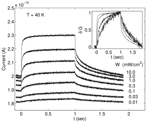
Fig. 1 shows typical time evolution curves of photoconduction of o-TaS3. Photoresponse at K is relatively slow with intensity-dependent relaxation time of millisecond region. No fast contribution with expected picosecond relaxation time comment is observed. Inset in Fig. 1 shows the same curves normalized to their amplitudes. The shape of the curves depends on the light intensity and relaxation is getting faster for more intensive light. The photocurrent is a nonlinear function of the light intensity: e.g. growth of from 0.1 to 0.3 mW/cm2 results in approximately the same increase of as growth of from 0.3 to 1 mW/cm2 (Fig. 1).
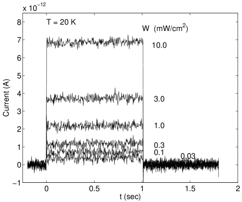
The intensity range where slow response is observed is shifted to smaller light intensities upon cooling, and the response at a fixed light intensity is getting faster. Finally, at sufficiently low temperatures the photoconduction relaxation time is much faster than the time constant of our amplifier (0.3 ms) and the shape of the response does not look intensity dependent (Fig. 2). Detailed study of temperature evolution of photoconduction kinetics proves that the fast low-temperature response can be considered as the limiting case of very high light intensity.
The amplitude of photoconduction measured by the light modulation method is found to be a nonlinear function of the light intensity (Fig. 3). At K it can be approximated as , in contrast to with temperature dependent () for steady light illumination zzminajetpl . This law corresponds to so-called quadratic recombination which is intrinsic for semiconductors in the high-intensity limit ryvkin ; moss . In semiconductors the low-intensity limit () is characterized by the linear relation , and the crossover between the linear and quadratic recombination occurs at . Therefore, to determine the carriers responsible for photoconduction in o-TaS3, it is worth to search for the linear recombination region at much lower intensities.
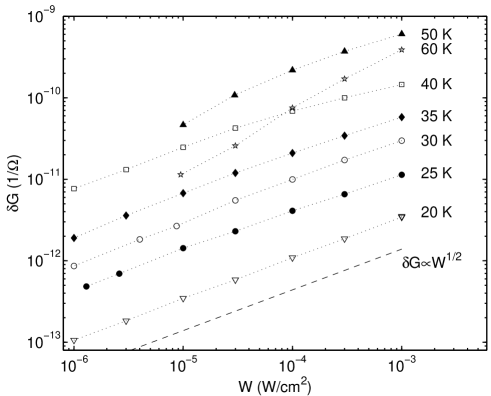
Fig. 4 shows temperature dependence of the linear conductance of o-TaS3 together with AC photoconductance measured by the standard light modulation technique in the temperature range K. curve is usual for this material. It consists of the high-temperature metallic part, the Peierls transition at 210 K (shifted due to the finite-size effect zzreview ), activation region with the activation energy 850 K corresponding to the half of the high-temperature value of the Peierls gap , and the low-temperature region with the activation energy about 400 K.
To find the level of linear conduction for current carriers responsible for photoconduction we have to analyze curves more accurately. Inset in Fig. 4 shows the same set of curves normalized to the light intensity values. At K all curves collapse into a single curve which can be fitted by the activation law with the activation energy K. The temperature of deviation from this activation law decreases with decrease of . Similarly, normalization by collapses curves in the low-temperature region below 40 К, in agreement with Fig. 3. Thus, the maxima of dependences separate linear and nonlinear recombination regimes.
The concentration of electrons in semiconductors with quadratic recombination obeys the equation ryvkin ; moss
| (1) |
where is the quantum efficiency of photogeneration, is the absorption coefficient, and , and are respectively the electron and hole concentrations in and out of equilibrium, is a recombination coefficient and is a light intensity. The equation for hole concentration is similar. Let us assume for simplicity that , , where , . In the stationary state . We are looking for values for two cases: i) when , and ii) when . From equation 1 one gets: i) and ii) . So the ratio at is 1.5 times smaller than its value at .
In nonstationary case the signal amplitude depends also on the modulation frequency . The conduction does not reach its stationary value when the light is on and does not relax to its equilibrium value when the light is off (see, e.g. Fig. 1 at mW/cm2). The measured AC conduction modulation is therefore only a fraction of photoconduction of the stationary case. For data presented in Fig. 4 ( Hz) the crossover to nonstationary case takes place around 60 K, so s. At K , i.e. photoconduction measured at small light intensities is nonstationary.
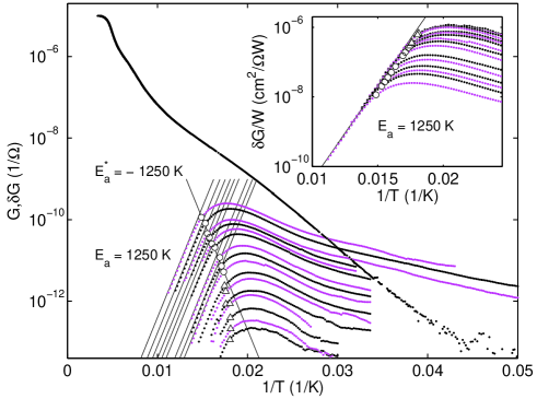
Open circles and triangles in the inset in Fig. 4 mark level which is 1.5 times smaller than the activation one for stationary (circles) and nonstationary (triangles) photoconduction. As it was argued above, in the stationary case the photoconduction at these points is equal to the linear conduction of photoconduction-providing current carriers. Corresponding values of are also shown in Fig. 4 by the same markers. The high-temperature part of the curve (circles, K) follows the activation dependence with the activation energy , and is much steeper in the nonstationary case (triangles).
The relaxation time can be found from the amplitude of photoconduction in the stationary state (we assume for simplicity that is much smaller than our sample thickness itkis )
| (2) |
As and are not expected to be temperature dependent, so in the linear relaxation regime (inset in Fig. 4) comment_tau . The characteristic time, , of the main dielectric relaxation process (-process) fitted in Ref. bel by the Vogel-Fulche law, at K has the same temperature dependence as observed here. was attributed to the temperature variation of quasiparticle concentration bel . Similarly, also follows quasiparticle concentration (see below). It is very likely, therefore, that these relaxations represent two sides of the same process of electron redistribution.
Recent interlayer tunneling experiments lat revealed step-like temperature dependence of the tunneling gap in o-TaS3 indicating appearance of a new low-temperature phase below 100 K, presumably corresponding to the commensurate CDW lat . This phase has a bigger value of the gap, K, than the high-temperature phase ( K), being very close to both and . In its turn, the interband radiative recombination lifetime (the process responsible for quadratic recombination) of semiconductors depends on the Fermi level position. In pure semiconductors , where is a semiconductor energy gap ryvkin ; moss . In doped semiconductors is much smaller and has much weaker temperature dependence ryvkin ; moss . In o-TaS3 () . Thus, photoconduction in o-TaS3 is provided by electrons and holes excited over the Peierls gap, and the Fermi energy is in the middle of the Peierls gap.
The origin of the low-temperature linear conduction with the activation energy much smaller the Peierls gap value is an adjacent question of interest. In principle, an additional conduction channel provided by hopping may shunt conduction of electrons and holes thermally excited over the Peierls gap. Hopping by impurity levels requires the Fermi level at impurity level hopping , i.e. about 400 K far from the Peierls gap edge, in contradiction with our conclusion about its middle-gap position. The variable-range-hopping mechanism implies a nonzero density of states near the Fermi level (non-zero for Mott-type conduction, and with a dip at the Fermi level for Efros-Shklovskii conduction hopping ). No middle-gap features are observed in the tunneling study lat . Hence, the low-temperature linear conduction of o-TaS3 is not provided by electrons and holes and is, therefore, of collective origin. This collective contribution dominates in the low-temperature linear conductivity and shunts the contribution of electrons and holes excited over the Peierls gap.
The possibility to distinguish between contributions of single-particle and collective excitations of the CDW (solitons) to the linear conduction is the most interesting result of the present study. We would like to note that photoexcitation of nonequilibrium electrons and holes may also change the soliton concentration and provide thereby a collective contribution into photoconduction which can be considered as a “collective photoconduction” collective . Interrelationship between the collective and single-particle photoexcitations is still an open question.
As it was mentioned above, the low-temperature deviation of from the activation law is a feature of many CDW and SDW materials. The method described here may help to clarify of the origin of this deviation in these materials, including, for example, the blue bronze K0.3MoO3 where photoinduced changes of nonlinear conduction and CDW creep rate are observed collective ; ogawa .
In conclusion, it is shown that photoconduction in quasi-one-dimensional conductors can be used as a probe of single-particle conduction. Our results demonstrate the presence of low-temperature collective conduction shunting single-particle conduction in o-TaS3.
Acknowledgements.
We are grateful to S. N. Artemenko and V. Ya. Pokrovskii for useful discussions and R. E. Thorne for providing high-quality crystals. The work was supported RFBR. These researches were performed in the frame of the CNRS-RAS-RFBR Associated European Laboratory “Physical properties of coherent electronic states in condensed matter” between CRTBT and IRE.References
- (1) P. Monceau, in: “Electronic Properties of Inorganic Quasi-one-dimensional Conductors”, Part 2. Ed. by P. Monceau. Dortrecht: D. Reidel Publ. Comp., 1985; G. Grüner, Rev. Mod. Phys. 60, 1129 (1988).
- (2) T. Sambongi, K. Tsutsumi, Y. Shiozaki, M. Yamamoto, K. Yamaya, and Y. Abe, Solid State Commun. 22, 729 (1977).
- (3) G. Grüner, Rev. Mod. Phys. 66, 1 (1994).
- (4) V.Ya. Pokrovskii, I. G. Gorlova, S. G. Zybtsev, and S. V. Zaitsev-Zotov, J. Phys IV (France), 131, 185 (2005).
- (5) G. Minton and J. W. Brill, Phys. Rev. B 45, 8256 (1992).
- (6) S.V. Zaitsev-Zotov, V.E. Minakova, Pis’ma v ZhETP, 79, 680 (2004) [JETP Letters, 79, 550 (2004)].
- (7) S.V. Zaitsev-Zotov, Physics – Uspekhi, 47, 533 (2004).
- (8) S.V. Zaitsev-Zotov, Microelectr. Eng., 69, 549 (2003).
- (9) M.E.Itkis, private communication.
- (10) M.E.Itkis, F.Ya. Nad, Pis’ma v ZhETP, 39, 373 (1984).
- (11) Theoretical predictions brazovskii give the energy relaxation time of nonequilibrium carries s. Reflection relaxation kinetics study in K0.3MoO3 by optical methods bbrelax demonstrates picoseconds relaxation scale for photoexcited carries.
- (12) S. A. Brazovskii, Zh. Exp. Teor. Fiz. 78, 677 (1980).
- (13) J. Demsar, K. Biljaković, and D. Mihailović, Phys. Rev. Lett. 83, 800 (1999).
- (14) S. M. Ryvkin, “Photoelectric phenomena in semiconductors” (in Russian), Fiz. Mat. Giz., Moscow (1963).
- (15) T. R. Moss, G. J. Burrel, B. Ellis, “Semiconductor Opto-Electronics”, Butterworth & Co Ltd (1973).
- (16) Taking , where cm-3 and 1/ are respectively electron concentration and conductance at K, cm2/W, m, and , one gets a rough estimate s, much closer to observed value 0.1 s, than the theoretical prediction brazovskii and the blue bronze data bbrelax .
- (17) D. Staresinić, K. Biljaković, W. Brütting, K. Hosseini, P. Monceau, H. Berger, and F. Levy, Phys. Rev. B 65, 165109 (2002).
- (18) Yu. I. Latyshev, P. Monceau, S.A. Brasovskii, A.P. Orlov, A.A. Sinchenko, Th. Fournier, and E. Mossang, J. Phys. IV, 131, 197 (2005).
- (19) B. I. Shklovskii and A. L. Efros, “Electronic Properties of Doped Semiconductors”, (Springer-Verlag, Berlin), 1984.
- (20) N. Ogawa, K. Miyano, S.A. Brazovskii, Phys. Rev. B. 71, 075118 (2005).
- (21) N. Ogawa, A. Shiraga, R. Kondo, S. Kagoshima, K. Miyano, Phys. Rev. Lett. 87, 256401 (2001).