Abstract
We show theoretically that finite two-dimensional (2D) photonic crystals in thin semiconductor membranes strongly modify the spontaneous emission rate of embedded dipole emitters. Three-dimensional Finite-Difference Time-Domain calculations show over 7 times inhibition and 15 times enhancement of the emission rate compared to the vacuum emission rate for judiciously oriented and positioned dipoles. The vertical index confinement in membranes strongly enhances modifications of the emission rate as compared to vertically unconfined 2D photonic crystals. The emission rate modifications inside the membrane mimic the local electric field mode density in a simple 2D model. The inhibition of emission saturates exponentially as the crystal size around the source is increased, with a length that is inversely proportional to the bandwidth of the emission gap. We obtain inhibition of emission only close to the slab center. However, enhancement of emission persists even outside the membrane, with a distance dependence which dependence can be understood by analyzing the contributions to the spontaneous emission rate of the different vertically guided modes of the membrane. Finally we show that the emission changes can even be observed in experiments with ensembles of randomly oriented dipoles, despite the contribution of dipoles for which no gap exists.
Spontaneous emission rates of dipoles in photonic crystal membranes
A. Femius Koenderink
Laboratory of Physical Chemistry, Swiss Federal Institute of Technology (ETH), 8093 Zürich, Switzerland
Maria Kafesaki
Institute of Electronic Structure and Laser (IESL), Foundation for Research and Technology Hellas (FORTH), P.O. Box 1527, 71110 Heraklion, Crete, Greece, and Dept. of Materials Science and Technology, Univ. of Crete, Greece.
Costas M. Soukoulis
Ames Laboratory, Iowa State University, Ames, Iowa 50011, and Institute of Electronic Structure and Laser (IESL), Foundation for Research and Technology Hellas (FORTH), P.O. Box 1527, 71110 Heraklion, Crete, Greece, and Dept. of Materials Science and Technology, Univ. of Crete, Greece.
Vahid Sandoghdar
Laboratory of Physical Chemistry, Swiss Federal Institute of Technology (ETH), 8093 Zürich, Switzerland
OCIS codes: 130.130, 160.0160,270.5580
1 Introduction
The last decade has seen a remarkable increase in the experimental efforts to control spontaneous emission dynamics of dipole transitions by tailoring the dielectric surroundings of the source. While studies in elementary geometries, such as planar interfaces[1, 2, 3, 4, 5, 6] or spherical particles[7, 8, 9, 10], remain of current interest, particular impetus in spontaneous emission control derives from solid state cavity quantum electrodynamics (CQED)[6, 11], and the increasing capability to shape semiconductors on the nanometer scale. Of particular interest in this respect are photonic band gap materials[12]. As first proposed by Bykov[13] and Yablonovitch[14], three-dimensionally periodic arrangements of dielectric material on wavelength-sized length scales allow to create a medium in which spontaneous emission processes can not only be enhanced but also completely inhibited. These photonic crystals offer many exciting prospects in fundamental physics, ranging from CQED, control of black-body radiation[15] and the slowing and storage of light [16], as well as device opportunities [12] for producing and processing of optical signals on sub-micron length scales.
Although efforts in realizing spontaneous emission control in three-dimensional (3D) photonic band gap crystals have been partly successful[17, 18, 19], the advantages of easier fabrication and characterization has motivated many groups to work on lower-dimensional, i.e., two-dimensional (2D) crystal structures. Photonic crystals in thin semiconductor membranes have recently shown particular promise to realize ultrasmall cavities with very high quality factors, suited for quantum optics in the strong coupling limit[20, 21, 22]. In addition, the first experimental evidence[23, 24, 25] for large emission inhibition of quantum dots and quantum wells in photonic crystal membranes has recently been reported. Although all these results suggest that the effect of the gap in the in-plane band-structure is greatly enhanced by the vertical index contrast, a systematic study of the potential for spontaneous emission rate control offered by membrane photonic crystals is lacking.
In this Paper we present a theoretical study of the spontaneous emission rate modifications in membrane photonic crystals that consist of only a finite number of unit cells. Such an analysis is particularly challenging for structures that are limited in size because approaches that are based on the commonly used plane-wave electromagnetic eigenfunction calculations[26, 27, 28, 29, 30, 31] cannot be used. We have therefore used a method similar to that recently proposed by Hwang et al.[32], Xu et al.[33, 34] and Hermann and Hess[35], based on the three-dimensional finite difference time-domain method (FDTD)[36].
The paper is organized as follows: in Section 2 we summarize our theoretical approach and discuss the numerical characteristics of the method. In Section 3 we discuss the spontaneous emission lifetime modification for a dipole in the center of a photonic crystal membrane, and compare our result to both 2D and 3D plane wave calculations of the local density of states. In Section 4 we focus on the dependence of the emission lifetime on the orientation of the transition dipole moment and the position of the emitter in the central plane of the membrane. In section 5 we consider the role of the crystal size in determining the spontaneous emission rate, and propose a relation between the width of the emission gap and the number of crystal rows that need to surround the emitter to obtain maximum inhibition. In section 6, we focus on the effect of membrane thickness and of the height of the dipole above the membrane center on the emission lifetime. We show that a simple model for the emission rate in homogeneous dielectric slabs explains many of the observed features. Finally, in Section 7 we discuss the prospects for experiments involving localized ensembles of emitters with randomly distributed dipole moments. Conclusions are presented in Section 8.
2 Method
The quantum analysis of spontaneous emission based on Fermi’s Golden Rule asserts that the spontaneous emission rate of an emitting dipole varies with its position and orientation , depending on the availability of photon modes at the source position and frequency . The central quantity that takes this into account is the local radiative density of states[37] (LRDOS) . The LRDOS is a classical electromagnetic quantity that appears in the classical analysis of radiating antennas, where it describes the power needed to drive a point-like electric dipole oscillating at fixed current[32, 33, 34, 35]. This power is due to the work that the field radiated by the source does on the source itself. The rate of spontaneous emission in a dielectric structure, normalized to the free-space rate , therefore can be found by comparing the work done on the source in the dielectric structure to the work done on the same current source in vacuum.
We use the three-dimensional finite different time domain method (FDTD) method for our calculations throughout this work. An important advantage of the finite difference time domain method[33, 34, 35, 36] over conventional methods[2, 28, 29] to calculate the LRDOS is that the field of a point source, and hence the LRDOS, is readily calculated without solving for the electromagnetic eigenmode basis of the dielectric structure. Furthermore, the FDTD method can even be used to calculate the LRDOS for lossy systems in which eigenmode expansions are invalid. In this paper we follow the method of Hermann and Hess [35], in which the LRDOS is simulated for a wide frequency range at once via broadband temporal excitation of a dipole point source. For a pulsed source with frequency spectrum , the time-trace of the electric field at the position of the source can be Fourier transformed to determine the LRDOS in terms of its vacuum value :
| (1) | |||||
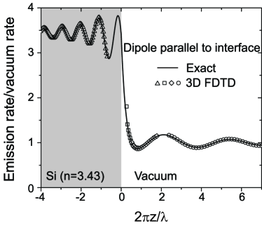
We have evaluated the validity and pitfalls of this numerical method by comparing the simulated spontaneous emission rate enhancement with exact analytical results for a dipole in a dielectric sphere[7, 8, 9, 35], and for a dipole near a planar interface between two dielectrics[2, 3, 4]. Figure 1 shows that accurate results for the emission rate modification are obtained by the FDTD method for a representative test case where a dipole is placed near a planar interface between air and silicon. By examining the LRDOS obtained with pulses at different center frequencies, we have established that results consistent to within can be obtained in the frequency ranges where the vacuum emission power of the dipole current pulse exceeds of its maximum value. Throughout this paper we use temporal excitation pulses with a Gaussian envelope and bandwidths around 50% of the central frequency.
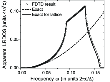
Agreement of the simulated LRDOS with the exact LRDOS not only depends on sufficient spectral overlap of the input current with the frequency range of interest, but also on the spatial discretisation. Apart from the obvious requirement that the discretisation must be sufficiently fine to resolve features of the dielectric structure, the accuracy is affected by the dispersive properties of the cubic discretisation grid itself. To illustrate this point, Fig. 2 shows the apparent LRDOS of a homogeneous dielectric of index over a very wide frequency range, obtained by the procedure described in Eq. (1). The exact LRDOS of the homogeneous dielectric (parabola in Fig. 2) equals times the vacuum LRDOS, independent of frequency. In contrast, Fig. 2 shows that large discrepancies occur for large frequencies. The deviation exceeds 5% for frequencies at which the wavelength in the dielectric is shorter than , where is the spacing between adjacent discretisation grid points. The source of the discrepancy is the well-known anisotropic dispersion of the cubic grid as well as the cut-off of the grid for wave vectors in excess of . We have calculated the density of states of the discretisation grid (filled with vacuum and with medium of index ) from its dispersion relation,[36]
| (2) | |||||
where is the magnitude of the time step, is the grid spacing, and is the speed of light in vacuum. The excellent agreement of the grid density of states with the apparent LRDOS calculated by the FDTD method for a dipole in a homogeneous dielectric in Fig. 2, confirms the role of the density of states of the numerical discretisation grid in spontaneous emission rate calculations. We conclude that an accuracy better than for spontaneous emission rates calculated by the FDTD method, requires discretisation grids with over 10 grid points per wavelength at the frequency of interest in the highest index medium.
Finally we note that accurate results require that the Fourier transforms of and be calculated without zero-padding of the time series, as done by many FFT routines that use arrays of length equal to a power of . To find the power spectrum radiated by the dipole, the complex Fourier transforms of the real time series of and are combined according to
| (3) |
The two terms are nearly equal in magnitude but opposite in sign. The desired sum is approximately times smaller than either term. Even if time-stepping is continued till the fields have decayed by several orders of magnitude, zero padding introduces noise that is small compared to either term in Eq. (3), but sizeable compared to the signal that remains after summing them. Furthermore, strongly resonant features in LRDOS spectra need to be handled with care. Time series of field and current are typically limited to total time spans of only to optical cycles, as the 3D FDTD method is very computationally intensive. For resonances with quality factors in excess of , time series are truncated before fields have fully decayed, giving rise to artifacts in the Fourier transform that can fully dominate the simulated LRDOS spectra. To remove such artifacts, we have used a seventh order Daubechies apodization filter [38]. We have checked the validity of this approach for FDTD simulations of a single-mode high-Q photonic crystal cavity [39], which has a much narrower resonance in the LRDOS than appears in any of the results presented below. For such a single mode system, the time series of the field can be extrapolated to obtain the true LRDOS from an untruncated time series.
3 Comparison with 2D and 3D LRDOS for vertically infinite crystals
We consider spontaneous emission rate modifications in two-dimensional photonic crystals within semiconductor membranes, as studied for the dipole-position averaged case by Lee and Yariv [34]. We focus on finite structures consisting of membranes with dielectric constant and thickness nm perforated with a hexagonal lattice of holes (lattice spacing nm) of radius . Such membranes have a wide band gap for TE guided modes, i.e., modes with electric field in the central plane of the slab pointing along the membrane, but no gap for TM modes. The geometrical parameters are typical for the membrane structures in which high-quality factor cavities for strong coupling CQED were recently realized[20, 21, 22] and for which first evidence of inhibition of spontaneous emission was recently presented[23, 24].
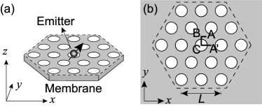
We simulate finite crystallites of hexagonal shape and various sizes ranging from 1 to 12 lattice spacings in radius, as counted from the central hole (see Fig. 3). The crystals were either terminated by semiconductor or by air extending into the Liao absorbing boundary conditions. We have used 14 or 20 grid points per lattice constant, with a doubled grid density in the vertical direction. To reduce staircasing errors due to the discretisation of the structure, we used volume-averaging of the dielectric constant in each grid cell[40]. In the simulations, membranes were surrounded above and below by up to 1m of air.
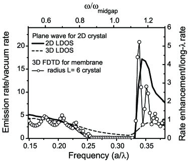
First, we consider the spontaneous emission lifetime for a dipole that is located in the middle of the central air hole of a structure of lattice spacings across. Figure 4 shows the LRDOS normalized to the vacuum LRDOS for an in-plane oriented dipole that points along the -axis (see Fig. 3), i.e., from air hole to air hole. For dipole orientations in the plane of the slab, the spontaneous emission rate is strongly modulated as a function of normalized frequency (where is the vacuum wavelength). We find a frequency range from to of inhibition of the emission rate that overlaps with the in-plane photonic band gap for the TE modes guided by the membrane, as was also observed in calculations by Lee, Xu and Yariv [34]. An inhibition of the LRDOS by a factor compared to vacuum is obtained. This value translates to over times inhibition as compared to the emission modification at frequencies far below the band gap at the same position. Above and below the range for which the emission is strongly reduced, which we will call emission gap, the emission rate is strongly modulated, featuring enhancements of the emission rate by factors up to 20 times compared to vacuum, or over times compared to the LRDOS in the long wavelength limit at the same position. As will be discussed below, the fringes outside the emission gap are due to Fabry-Pérot oscillations caused by the finite lateral size of the crystal.
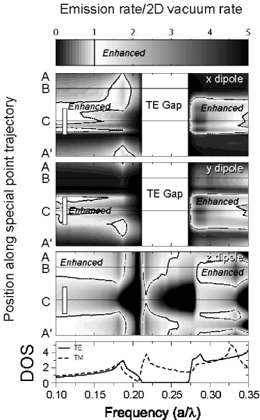
It is perhaps surprising that significant control over spontaneous emission dynamics is possible for selected dipole positions and orientations, despite the fact that no full band gap exists. It appears that the large vertical index contrast greatly enhances the effect of the in-plane periodicity on spontaneous emission. To confirm this notion, we have used the H-field inverted matrix plane-wave expansion method to calculate the local radiative density of states in infinite 2D photonic crystals that are not confined vertically[26, 28, 29]. In addition to the 3D LRDOS, wee have also calculated the 2D LRDOS, which only counts modes that propagate in the plane of periodicity. For the two (three)-dimensional case, we used 8100 (84000) non-equivalent k-points[41, 42], which were distributed over half of the full Brillouin zone to avoid erroneous results[28] due to the reduced symmetry of the polarization-resolved LRDOS[31]. We have scaled both the frequency axis and vertical axis to optimally overlap the resulting 2D and 3D LRDOS (normalized by the 2D resp. 3D vacuum LRDOS) for an -oriented dipole in the center of an air-hole with the LRDOS in the membrane (cf. Fig. 4). Naturally, the 2D (local) density of states of the 2D crystal shows a full gap for dipole orientations in the plane of periodicity, corresponding to the TE band gap in the 2D band structure. The gap is accompanied by characteristic emission enhancement at the gap edges due to low group velocity modes[28]. For a dipole at the center of an air hole, this enhancement occurs at the high frequency edge of the gap, as is also apparent in the membrane. In stark contrast, the 3D LRDOS is only weakly modulated for vertically infinite crystals, due to the contributions of modes with wave vector components along the air cylinders[43, 44]. Although the 2D band gap causes a shallow minimum in the 3D LRDOS for a dipole in the center of an air-hole, the bandwidth of emission inhibition is much narrower than the bandwidth of the 2D band gap, and no sign of emission enhancement at the band gap edges remains[28, 44]. The comparison of plane wave calculations with the FDTD result shows that the vertical confinement offered by membranes prevents the washing out of the characteristic features of the 2D LRDOS that occurs for vertically unconfined crystals: Firstly the emission gap in the membrane referenced to the long wavelength LRDOS at the same position in the crystal amounts to an inhibition by a factor around 30, which is over five times stronger than the inhibition obtained if the structure is not truncated in the vertical direction. Secondly, the relative inhibition gap bandwidth of 24% offered by the membrane structure is close to the bandwidth of 25% in the 2D band-structure. Thirdly, we note that the emission rate enhancement at the blue edge of the gap is retrieved in the membrane structure. The enhancement of times compared to the emission rate in the long wavelength limit is in good agreement with the enhancement observed in the 2D LRDOS. This is especially surprising, when considering the finite size of the crystal, and the effect of its truncation on the exact spectral position and quality factor of the Fabry-Pérot oscillations.
4 Dependence on polarization and lateral position
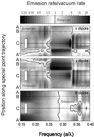
To obtain a more complete overview of the spontaneous emission control offered by membranes, we consider the LRDOS modification for different positions in the central unit cell of a crystallite that is again in radius, terminated on the sides by semiconductor material. Figure 5 shows contour plots of the LRDOS normalized to the vacuum LRDOS as a function of frequency in the range of the TE-bandgap, for dipoles that are vertically centered in the membrane and positioned along the path indicated in Fig. 3(b). This trajectory spans the boundary of the irreducible part of the real space 2D unit cell and ensures that the cartesian dipole orientations in Fig. 5 are always parallel or perpendicular to the trajectory. Figure 5 confirms the occurrence of a deep gap in the spontaneous emission rate for dipole orientations in the plane of the membrane for all positions close to the center of the crystal. Moreover we find that there is no gap in the emission rate for dipoles oriented perpendicular to the membrane, but only a weak dependence on frequency, as expected from the absence of a 2D band gap for the TM guided modes of the membrane.
A detailed inspection of Fig. 5 shows furthermore that strong emission enhancement at the blue edge of the emission gap is only predicted to occur for dipoles positioned inside the air hole . In contrast, emission enhancement at the red edge of the gap is only predicted for dipoles located outside the air-hole, and preferentially for dipoles oriented perpendicular to the air-hole edges. This difference between dipole positions inside and outside the air holes is confirmed by the 2D LRDOS modification predicted by the plane wave method (Fig. 6) and is consistent with the well-known difference in spatial distribution of the low group-velocity modes that cause the spontaneous emission enhancement. These modes are preferentially concentrated in the air (dielectric) region for the high (low) frequency edge of the gap. Disregarding the Fabry-Pérot oscillations due to the finite crystal size, we find that the spectral and spatial location of the enhancements, the relative magnitude of the enhancements compared to the LRDOS modifications for frequencies far below the gap, as well as the band width of the gap in Fig. 5(a,b) are in good qualitative agreement with the 2D LRDOS modification calculated by the plane-wave method (Figure 6).
It should be noted that good agreement is limited to dipole orientations parallel to the membrane, as the vertical confinement in the membrane causes a much larger shift to higher frequencies for the photonic band structure for TM polarization than for TE polarization[45]. The results in Fig. 5 do not agree for any polarization with the much weaker 3D LRDOS modification for a crystal that is infinitely extended in the vertical direction.
5 Emission Gap width and the crystal size required for maximum emission gap depth
Figures 4 and 5 allow us to conclude that large changes in spontaneous emission rate occur for properly oriented dipoles located near the center of small crystals in semiconductor membranes. In this section we investigate how large the crystal around the dipole must be to obtain a significant emission gap. In Fig. 7 the spontaneous emission modification is shown for a horizontally -oriented dipole in the central air holes of semiconductor-truncated crystals of various sizes. The most striking features in Fig. 7 are the deepening of the emission gap with increasing size of the crystallite around the source, the steepening of the emission gap band edges, and the decrease of the frequency spacing between modulations of the emission rate outside the emission gap.
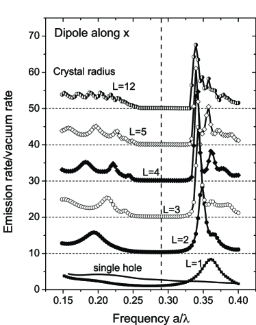
The decreasing frequency spacing between these fringes with increasing crystal size validates their interpretation as Fabry-Pérot type resonances caused by the impedance mismatch occurring at the outer edges of the crystal. When crystals are truncated by air rather than semiconductor, the oscillations change in amplitude and shift in frequency at unchanged frequency spacing between fringes, as consistent with an interpretation as Fabry-Pérot resonances. Unlike the Fabry-Pérot oscillations that occur for transmission through finite crystals[46, 47], however, the oscillations in the LRDOS depend on all size-dependent resonances in the system, instead of solely those with specific wave vectors. Independently of the size and nature of the truncation, the LRDOS at the high frequency edge of the emission gap exceeds times the vacuum LRDOS, corresponding to an enhancement of at least times compared to the emission rate typically observed below the gap in the range .
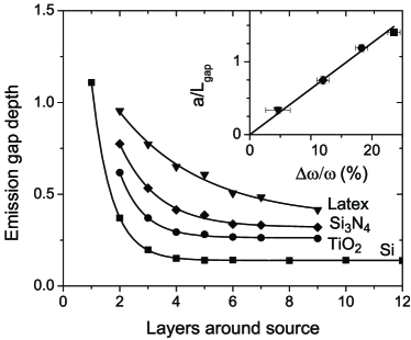
The value of the LRDOS for frequencies within the emission gap saturates with increasing crystal size. In Fig. 8, we plot the emission inhibition gap minimum for the frequency in the middle of the emission gap as a function of crystal radius. The LRDOS in the middle of the gap decreases exponentially[43, 35, 48] to its limiting value of 0.14 times the vacuum value, with a crystal radius of just . It is remarkable that only so few crystal layers are needed to create the emission gap. This observation suggests that the emission gap can be expected to be very robust against fabrication disorder. The radius for the emission gap can be compared to the number of layers needed for a cavity to reach its ultimate quality factor. The inverse quality factor of low volume microcavities in 2D photonic crystals approaches its limiting value set by the out-of-plane losses in an exponential manner as the number of crystal rows surrounding the cavity is increased[45, 49]. For unoptimized and optimized single-hole cavities [21, 39, 45] operating at frequencies in the middle of the band gap, the same characteristic length of is found for the inverse quality factor.
Figure 8 also shows the gap minimum as a function of crystal size for photonic crystal membranes of different dielectric constants (titanium dioxide, nm), (silicon nitride, nm) and (polystyrene, nm). As expected, the maximum achievable inhibition decreases with reduced index contrast, and the characteristic number of layers needed to achieve the inhibition increases with decreasing refractive index contrast. The inset in Fig. 8 shows the inverse characteristic length as a function of the relative band width of the emission gap. We observe that is inversely proportional to the width of the band gap. This inverse dependence is well known for the penetration depth of light in dielectric mirrors, and for simple two-band models of Bragg diffraction from photonic crystal lattice planes [46]. In such a model the field intensity decays exponentially into the crystal, with intensity decay length where is the separation between lattice planes. The same behavior is found for , as shown by quantitative comparison of taken from the FDTD simulations with . This observation highlights the universal role of the gap width as a measure for the interaction strength of the photonic structure with light, as proposed in Ref. 48, 50. A more thorough investigation of this hypothesis should include calculations for 2D and 3D photonic crystal geometries and is outside the scope of this paper.
6 Different contributions to the emission rate derived from a simple homogeneous slab model
Figure 8 not only shows that the emission gap in membrane photonic crystals deepens exponentially with lateral crystal size, but also that the inhibition that is ultimately achieved for sufficiently large crystals depends on the membrane index. Similarly, we expect the emission gap depth to depend on the thickness of the membrane. We have calculated the spontaneous emission rate for a dipole in the central air hole of photonic crystal membranes as considered in Fig. 4 ( nm, ) for membrane thicknesses between and nm. Figure 9 shows the emission rate normalized to the vacuum rate at the center frequency of the emission gap, which shifts from at nm to lower frequencies as the membrane thickness increases. The center frequency of the gap saturates at around for thicknesses around nm. For membrane thicknesses above nm contributions of higher order slab guided modes compromise the definition of the gap edges that allows us to find the center frequency. For these thicknesses the Fabry-Pérot oscillations for frequencies just below the red edge of the gap merge with Fabry-Pérot oscillations for in-gap frequencies. The enhancement at the blue edge of the gap remains clearly visible and remains above 10 times the vacuum LRDOS. For thicknesses above nm the emission rate modulation in the frequency range around the gap approaches an asymmetric sawtooth like shape, similar to the 3D LRDOS in a vertically infinite crystal (Figure. 4).
Figure 9 shows that significant inhibition of emission occurs for membrane thicknesses below nm, with an optimum thickness for inhibition around nm. For larger thicknesses, the emission rate is significantly less inhibited, and even enhanced for nm. As a simple model to explain the thickness dependence of the emission rate, we consider the emission rate of dipoles in homogeneous dielectric slabs. We have used the approach of Urbach and Rikken [51] that allows to separate the contributions to the LRDOS of modes that propagate outside the dielectric slab from the contributions of the slab guided modes to the lifetime of in-plane oriented dipoles. In a high index dielectric slab, such as a silicon membrane in air (Fig. 9, inset) the LRDOS contribution of propagating modes is strongly reduced to only times the vacuum LRDOS. However, the LRDOS contribution of the guided modes causes the overall LRDOS, and hence the spontaneous emission rate for an embedded dipole to exceed the vacuum LRDOS significantly.
For a photonic crystal membrane that has a full band gap for the first TE slab-guided mode, one expects the LRDOS contribution of the first TE guided mode to vanish completely. To assess the validity of this hypothesis, we plot the mid-gap emission rate in Fig. 9 as a function of normalized thickness in the inset of Fig. 9 and compare it to the LRDOS in a homogeneous silicon slab, without the contribution of the first TE guided mode. The comparison reveals that the emission rate in the emission gap of Si photonic crystal membranes indeed follows qualitatively the same dependence on slab thickness as the LRDOS in a homogeneous silicon membrane without the contribution of the first TE guided mode, yet shifted towards larger thicknesses. The sharp increase of the emission rate with thickness around allows us to fit an effective refractive index of for which the LRDOS at gap frequencies of the membranes most resembles the LRDOS without the first TE guided mode contribution in unpatterned dielectric slabs. This value is higher than the effective index of derived from the volume averaged dielectric constant of the membrane. It is important to note, however, that the sharp increase of the emission rate is due to the combined contributions of the second order TM and the third order TE slab guided mode, for which the derivation of an effective index is highly nontrivial.

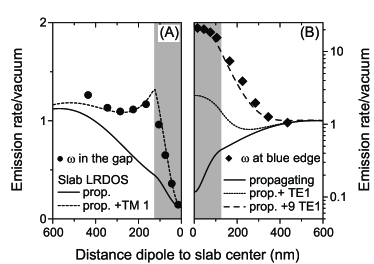
The interpretation of lifetimes in photonic crystal membranes in terms of the propagating and guided mode LRDOS contributions in a dielectric slab is also relevant for the dependence of the LRDOS on the separation of the dipole from the center of the photonic crystal membrane. In Fig. 10 we plot the emission rate at two key frequencies for an -oriented dipole in the central air hole of a membrane of nm thickness that is shifted vertically above the center of the slab. For a frequency in the emission gap (Fig. 10(a)) we find that the inhibition of emission quickly vanishes as the dipole is moved away from the center of the slab. No traces of inhibition remain for dipoles that are further than nm away from the slab center. In contrast, we find that the enhancement at at the blue edge of the gap is not restricted to dipole positions within 100 nm of the slab center. Emission enhancement by a factor persists even nm above the slab, as we proposed recently [52]
The differences in persistence of the inhibition and of the enhancement of spontaneous emission with increasing separation of the emitter to the slab can also be understood by analyzing the various guided mode contributions to the LRDOS of a homogeneous slab. For the frequency in the gap, no contribution to the LRDOS of the first TE guided mode exists, due to the TE band gap. In this frequency range, the only other modes that contribute to the LRDOS in a dielectric slab are the propagating modes and the first TM guided mode. The electric field component parallel to the membrane of the first TM guided mode is zero in the center of the slab, but increases monotonically towards the edge of the slab. Indeed, we find excellent agreement of the LRDOS calculated by FDTD for -oriented dipoles in the membrane, and the sum of LRDOS contributions of propagating modes and the first TM guided mode in a dielectric slab of index , equal to the volume average refractive index of the photonic crystal. In essence, the range of dipole heights over which inhibition occurs is limited by the parallel electric field profile of the first TM slab mode. In contrast, the enhancement of emission at the blue edge of the gap is due to the photonic crystal induced enhanced density of first order TE guided modes. The emission enhancement as a function of dipole height therefore traces the vertical mode profile of the first TE guided mode. This notion is confirmed by the fact that the enhancement in Figure 10(b) for a PC membrane, can be excellently described as the sum of the propagating mode LRDOS contribution in the effective index slab, augmented by a scaled contribution of the first TE guided mode. Quantitatively, we find that the contribution of the first TE guided mode is enhanced by times over the contribution of the same mode in a homogeneous slab of the same effective index.
7 Orientational dipole ensembles
Single quantum emitters that are controlled in position and dipole orientation are required to experimentally confirm the strong dependence on position and polarization of the spontaneous emission rate predicted by the simulations. However, the preparation, manipulation and detection of high-quantum efficiency single emitters face many experimental challenges in the near-infrared range where most photonic crystals operate best. In such experiments, we therefore expect that ensembles of emitters are likely to be used[53]. In this section we evaluate the emission rate modification that is observable for a subwavelength-sized orientationally isotropic ensemble of dipoles located in the central air hole of the photonic crystal membrane considered in Figs. 4 and 5. To obtain an angle-averaged modification of the emission rate for an isotropic ensemble of dipole orientations, one often uses a simple average of the LRDOS over three perpendicular dipole orientations[51]. However, because of the angle-dependence of the luminescence extraction efficiency[54] , such a simple average is not suited for reconstructing the ensemble-averaged emission rate modification that is observable with far-field collection optics. The fraction of light emitted into propagating waves instead of the guided mode of the slab depends strongly on dipole orientation. For example, a dramatic increase of the emission extraction efficiency from for frequencies below the gap to above 80% in the gap occurs for in-plane dipoles. This increase counteracts the reduction in visibility of the emission gap that is naively expected due to the contribution of vertically oriented dipoles.
To assess the changes in the emission dynamics observable in time-resolved fluorescence measurements, we have calculated the LRDOS and for differently oriented dipoles in the central air hole. We obtained from the frequency-dependent Poynting vector using on-the-fly discrete Fourier transform of the time-dependent tangential E and H-fields on the surface of a box enclosing the crystal structure.[36] To synthesize the observable ensemble-averaged decay dynamics, one needs to average exponential time traces with decay rate set by the LRDOS and weighting factor proportional to over all possible dipole orientations (described by polar angles and ):
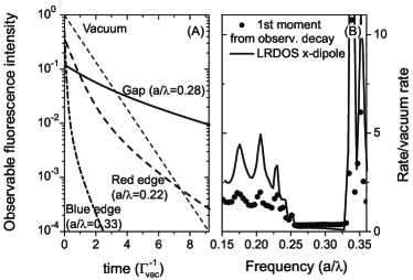
Here, time is in units of the vacuum decay time, and is the orientation-dependent emission rate normalized to the vacuum emission rate. We have approximated this integral by averaging over more than 300 orientations in solid angle, corresponding to over 25 inequivalent dipole orientations. In general, we obtain strongly non-single exponential time traces for the ensemble decay. Fig. 11(a) presents the fluorescence decay for three key frequencies and just below, in, and just above the emission gap. At the red edge of the gap the non-exponential decay reveals both an enhanced and an inhibited decay component. For frequencies inside the gap, we predict that the ensemble-averaged decay exhibits a clear slowing of the decay dynamics, while a substantial acceleration is predicted to be observable for frequencies at the blue edge of the gap. The non-exponential nature of the time traces, which for some frequencies is more pronounced than for the three traces shown in Fig. 11(a), requires that experiments be performed with sources for which the decay dynamics in a medium of unmodulated LRDOS is completely understood. Furthermore an analysis method to quantify the overall emission rate modification will be necessary. Here, we consider the first moment
of the synthesized fluorescence decay to quantify the overall emission rate modification evident in the nonexponential time traces. In Fig. 11(b) we plot the inverse of the first moment in units of the vacuum decay rate for different emission frequencies. We see that even the dipole orientation-averaged emission will reveal inhibition (enhancement) of the mean lifetime by a factor 3 (5) compared to vacuum.
8 Conclusions
We have used the three-dimensional Finite Difference Time Domain method to systematically investigate the spontaneous emission rate modifications that occur for emitters inside photonic crystal membranes. The spontaneous emission rate depends strongly on dipole position and orientation relative to the crystal lattice. In the central plane of the slab and for in-plane oriented dipoles, the full gap for the first TE guided mode of the vertical structure causes an inhibition of emission by more than seven times compared to vacuum over a large frequency window. In addition, large enhancements of the emission rate occur at the band edges. In the middle of the membrane, vertical index confinement causes the emission rate modifications to be much stronger than in vertically unconfined 2D crystals. The true 3D LRDOS in a photonic crystal membrane mimics the hypothetical 2D LRDOS of a 2D crystal in terms of the frequency band width of the gap, the magnitude of the enhancement (with respect to vacuum) at the band edges, and the variations of the LRDOS spectrum with lateral position of the dipole in the unit cell. While the LRDOS in the central plane of the membrane can be understood from the 2D band structure, the variation of the LRDOS with the height of the dipole from the center of the slab can be explained by considering the electric field mode profiles of the lowest few TE and TM guided modes supported by the thin membrane. This is especially relevant for applications that aim at enhancing spontaneous emission. Due to the vertical extent of the first TE guided mode of the membrane, sizeable emission rate enhancements due to the photonic crystal remain even outside the membrane. For various PC structures of different index contrasts, we have found that the emission rate inside the emission gap reduces exponentially with the system radius to a residual value that can be understood as the LRDOS contribution of modes propagating in air for a homogeneous dielectric slab of proper effective index. We have furthermore presented evidence that the crystal radius associated with the deepening of the emission gap scales inversely with the relative frequency band width of the gap in the 2D dispersion relation. Finally, we have also considered the role of ensemble averaging in experiments that use localized collections of emitters. A realization of such an experiment involves, for instance, a sub-wavelength ensemble of emitters[53] attached to the end of a sharp glass tip and positioned by using scanning probe techniques, acting as a controllable local probe of the emission modification. Such a sub-wavelength source averages over an isotropic random distribution of dipole orientations. Despite the presence of dipole orientations that do not match the gap for TE modes, we predict the first moment of the expected non-exponential times traces to show sizeable inhibition and enhancement of the mean emission rate.
Acknowledgments
We are grateful to Ben Buchler for stimulating discussion. Financial support by EU-projects DALHM, Metamorphose, Phoremost, as well as by DARPA (Contract number MDA972-01-2-0016)and Ames Laboratory are also acknowledged. This project was performed within the focus program SP1113 of the Deutsche Forschungsgemeinschaft (DFG). Femius Koenderink’s current address is FOM Institute for Atomic and Molecular Physics, Kruislaan 407 1098 SJ, Amsterdam, The Netherlands. He can be reached by e-mail at F.Koenderink@amolf.nl, and Vahid Sandoghdar can be reached by e-mail at vahid.sandoghdar@ethz.ch.
References
- [1] K. H. Drexhage, “Influence of a Dielectric Interface on Fluorescence Decay Time”, J. Lumin. 1, 693–701 (1970).
- [2] H. Khosravi and R. Loudon, “Vacuum Field Fluctuations and Spontaneous Emission in the Vicinity of a Dielectric Surface,” Proc. Roy. Soc. London 433, 337– 352 (1991)
- [3] E. Snoeks, A. Lagendijk, and A. Polman, “Measuring and modifying radiative transitions rate of erbium near an interface,” Phys. Rev. Lett. 74, 2459-2462 (1995).
- [4] R. M. Amos and W. L. Barnes, “Modification of the spontaneous emission rate of Eu3+ ions close to a thin metal mirror,” Phys. Rev. B 55, 7249–7254 (1997).
- [5] B. C. Buchler, T. Kalkbrenner, C. Hettich, and V. Sandoghdar, “Measuring the quantum efficiency of single radiating dipoles,” Phys. Rev. Lett. 95, 063003:1–4 (2005).
- [6] P. R. Berman, ed., Cavity Quantum Electrodynamics (Academic, San Diego, Calif., 1994).
- [7] H. Chew, “Radiation and lifetimes of atoms inside dielectric particles,” Phys. Rev. A 38, 3410–3416, (1988).
- [8] V. V. Klimov, M. Ducloy, and V. S. Letokhov, “Spontaneous emission rate and level shift of an atom inside a dielectric microsphere,” J. Mod. Opt. 43 549–563 (1996).
- [9] F. L. Kien, N. H. Quang, and K. Hakuta, “Spontaneous emission from an atom inside a dielectric sphere,” Opt. Commun. 178, 151–164 (2000).
- [10] H. Schniepp, and V. Sandoghdar, “Spontaneous Emission of Europium Ions Embedded in Dielectric Nanospheres,” Phys. Rev. Lett. 89, 257403:1-4 (2002).
- [11] K. J. Vahala, “Optical Microcavities”, Nature 424, 839–846 (2003).
- [12] C. M. Soukoulis, ed., Photonic crystals and light localization in the century (Kluwer Academic Publishers, Dordrecht, 2001).
- [13] V. P. Bykov, “Spontaneous Emission in a Periodic Structure,” Sov. Phys.–JETP 35, 269–273 (1972).
- [14] E. Yablonovitch,“Inhibited Spontaneous Emission in Solid-State Physics and Electronics,” Phys. Rev. Lett. 58, 2059–2062 (1987).
- [15] C. M. Cornelius and J. P. Dowling, “Modification of Planck blackbody radiation by photonic band-gap structures”, Phys. Rev. A 59, 4736–4746 (1999).
- [16] M. F. Yanik and S. Fan, “Stopping light all optically,” Phys. Rev. Lett. 92, 083901:1-4 (2005).
- [17] A. F. Koenderink, L. Bechger, H. P. Schriemer, A. Lagendijk, and W. L. Vos, “Broadband fivefold reduction of vacuum fluctuations probed by dyes in photonic crystals,” Phys. Rev. Lett. 88, 143903:1-4 (2002).
- [18] P. Lodahl, A. F. van Driel, I. S. Nikolaev, A. Irman, K. Overgaag, D. Vanmaekelbergh, and W. L. Vos, “Controlling the dynamics of spontaneous emission from quantum dots by photonic crystals,” Nature 430, 654–657 (2004).
- [19] S. P. Ogawa, M. Imada, S. Yoshimoto, M. Okano, S. Noda, “Control of light emission by 3D photonic crystals,” Science 305, 227–229 (2004).
- [20] Y. Akahane, T. Asano, B. S. Song, S. Noda, “ High-Q photonic nanocavity in a two-dimensional photonic crystal,” Nature 425, 944–947 (2003).
- [21] K. Srinivasan, P. E. Barclay, O. Painter, J. X. Chen, A. Y. Cho, C. Gmachl, “Experimental demonstration of a high quality factor photonic crystal microcavity,” Appl. Phys. Lett. 83, 1915–1917 (2003).
- [22] T. Yoshie, A. Scherer, J. Hendickson, G. Khitrova, H.M. Gibbs, G. Rupper, C. Ell, O.B. Shchekin D.G. Deppe, “Vacuum Rabi splitting with a single quantum dot in a photonic crystal nanocavity,” Nature 432, 200–203 (2004).
- [23] A. Kress, F. Hofbauer, N. Reinelt, M. Kaniber, H. J. Krenner, R. Meyer, G. Bohm, and J. J. Finley, “Manipulation of the spontaneous emission dynamics of quantum dots in two-dimensional photonic crystals,” Phys. Rev. B 71 241304, 2005.
- [24] D. Englund, D. Fattal, E. Waks, G. Solomon, B. Zhang, T. Nakaoka, Y. Arakawa, Y. Yamamoto, J. Vučković “Controlling the Spontaneous Emission Rate of Single Quantum Dots in a 2D Photonic Crystal,” Phys. Rev. Lett. 95 013904 (2005).
- [25] M. Fujita, S. Takahashi, Y. Tanaka, T. Asano, S. Noda , “Simultaneous inhibition and redistribution of spontaneous light emission in photonic crystals”, Science 308, 1296-1298 (2005).
- [26] K. M. Ho, C. T. Chan, and C. M. Soukoulis, “Existence of a photonic gap in periodic dielectric structures,” Phys. Rev. Lett. 65, 3152–3155 (1990).
- [27] T. Suzuki and P. K. L. Yu, “Emission power of an electric dipole in the photonic band structure of the fcc lattice,” J. Opt. Soc. Am. B 12, 570–582 (1995).
- [28] K. Busch and S. John, “Photonic band gap formation in certain self-organizing systems,” Phys. Rev. E 58, 3896–3908 (1998).
- [29] K. Busch, N. Vats, S. John and B. C. Sanders, “Radiating Dipoles in Photonic Crystals,” Phys. Rev. E 62, 4251–4260 (2000).
- [30] Z. Y. Li, L. L. Lin, and Z. Q. Zhang, “Spontaneous emission from photonic crystals: full vectorial calculations,” Phys. Rev. Lett. 84, 4341–4344 (2000).
- [31] R. Z. Wang, X. H Wang, B. Y Gu, and G. Z. Yang, “Local density of states in three-dimensional photonic crystals: calculation and enhancement effects,” Phys. Rev. B 67, 155114:1-7 (2003).
- [32] J.-K. Hwang, H.-Y. Ryu, and Y.-H. Lee, “Spontaneous emission rate of an electric dipole in a general microcavity,” Phys. Rev. B 60, 4688–4695 (1999).
- [33] Y. Xu, R. K. Lee, and A. Yariv, “Quantum Analysis and the Classical Analysis of Spontaneous Emission in a Microcavity,” Phys. Rev. A 61, 033807:1-13 (2000).
- [34] R. K. Lee, Y. Xu, A. Yariv, “Modified Spontaneous Emission from a two-dimensional Photonic Bandgap Crystal Slab,” J. Opt. Soc. Am. B 17, 1438–1442 (2000).
- [35] C. Hermann and O. Hess, “Modified Spontaneous Emission rate in an Inverted-opal Structure with Complete Photonic Bandgap,” J. Opt. Soc. Am. B 19, 3013–3018 (2002).
- [36] A. Taflove and S.C. Hagness, Computational Electrodynamics: The Finite-Difference Time-Domain Method (2nd ed., Artech House, Boston, MA, 2000).
- [37] R. Sprik, B. A. van Tiggelen, and A. Lagendijk, “Optical Emission in Periodic Dielectrics,” Europhys. Lett. 35, 265–270 (1996).
- [38] I. Daubechies, “Orthonormal Bases of Compactly Supported Wavelets,” Comm. Pure Appl. Math. 41, 909-996 (1988).
- [39] A. F. Koenderink, M. Kafesaki, B. C. Buchler, V. Sandoghdar, “Controlling the Resonance of a Photonic Crystal Microcavity by a Near-Field Probe”, Phys. Rev. Lett. 95, 153904:1–4 (2005).
- [40] O. Hess, C. Hermann and A. Klaedtke, “Finite-Difference Time-Domain simulations of photonic crystal defect structures,” Phys. Stat. Sol. A 197, 605–619 (2003).
- [41] G. Gilat,“Analysis of Methods for Calculating Spectral Properties in Solids,” J. Comput. Phys. 10, 432–465 (1972).
- [42] H. J. Monkhorst, and J. D. Pack, “Special Points for Brillouin-Zone Integrations,” Phys. Rev. B 13, 5188–5192 (1976).
- [43] A. A. Asatryan, K. Busch, R. C. McPhedran, L. C. Botten, C. M. de Sterke, . and N. A. Nicorovici, “Two-Dimensional Green’s Function and Local Density of States in Photonic Crystals Consisting of a Finite Number of Cylinders of Infinite Length,” Phys. Rev. E 63, 046612:1-4 (2001).
- [44] D. P. Fussell, R. C. McPhedran, C. M. de Sterke, and A. A. Asatryan, “Three-dimensional local density of states in a finite two-dimensional photonic crystal composed of cylinders,” Phys. Rev. E 67, 045601:1-4 (2003).
- [45] O. Painter, J. Vučković, and A. Scherer, “Defect modes of a two-dimensional photonic crystal in an optically thin dielectric slab,” J. Opt. Soc. Am. B 16, 275–285 (1999).
- [46] K.W.-K. Shung and Y. C. Tsai, “Surface effects and band measurements in photonic crystals,” Phys. Rev. B 48, 11265-11269 (1993).
- [47] Yu. A. Vlasov, M. Deutsch, and D. J. Norris, “Single-domain spectroscopy of self-assembled photonic crystals,” Appl. Phys. Lett. 76, 1627–1629 (2000).
- [48] J. S. Kole, New methods for the numerical solution of Maxwell’s equations, (PhD thesis, Rijksuniversiteit Groningen, The Netherlands (2003)) http://www.ub.rug.nl/eldoc/dis/science/j.s.kole/
- [49] M. Okano, A. Chutinan, and S. Noda, “Analysis and design of single-defect cavities in a three-dimensional photonic crystal,” Phys. Rev. B 66, 165211:1-6 (2002).
- [50] W.L. Vos, R. Sprik, A. van Blaaderen, A. Imhof, A. Lagendijk, and G.H. Wegdam, “Strong effects of photonic band structures on the diffraction of colloidal crystals,” Phys. Rev. B. 53, 16231-16235 (1996).
- [51] H. P. Urbach, and G. L. J. A. Rikken, “Spontaneous emission from a dielectric slab,” Phys. Rev. A 57, 3913–3930 (1998).
- [52] A. F. Koenderink, M. Kafesaki, C. M. Soukoulis, V. Sandoghdar, “Spontaneous emission in the near-field of 2D membrane photonic crystals,” Opt. Lett, 30, 3210–3212 (2005).
- [53] P. Olk, B. C. Buchler, V. Sandoghdar, N. Gaponik, A. Eychmüller, A. L. Rogach, “Subwavelength emitters in the near-infrared based on mercury telluride nanocrystals,” Appl. Phys. Lett. 84, 4732–4734 (2004).
- [54] S. Fan, P. R. Vileneuve, J. D. Joannopoulos, E. F. Schubert, “High extraction efficiency of epontaneous emission from slabs of photonic crystals”, Phys. Rev. Lett. 78, 3294–3297 (1997).