Spin Hall effect in clean two dimensional electron gases with Rashba spin-orbit coupling
Abstract
We study the spin polarization induced by a current flow in clean two dimensional electron gases with Rashba spin-orbit coupling. This geometric effect originates from special properties of the electron’s scattering at the edges of the sample. In wide samples, the spin polarization has it largest value at low energies (close to the bottom of the band) and goes to zero at higher energies. In this case, the spin polarization is dominated by the presence of evanescent modes which have an explicit spin component outside the plane. In quantum wires, on the other hand, the spin polarization is dominated by interference effects induced by multiple scattering at the edges. Here, the spin polarization is quite sensitive to the value of the Fermi energy, especially close to the point where a new channel opens up. We analyzed different geometries and found that the spin polarization can be strongly enhanced.
pacs:
72.25.Dc,73.23.-b,73.23.Ad,71.70.EjI Introduction
The possibility to create and manipulate spin currents or to induce spin polarization at the edges of a semiconductor by simply applying an external charge current has created great expectation in the field of spintronics—a fast developing area aimed to build up new technologies based on the manipulation of the electron’s spin.Awschalom et al. (2002) The phenomenon of current induced spin polarization (CISP)—also called spin Hall effect (SHE) when referred to the perpendicular polarization in two dimensional systems—was predicted some time ago by D’yakonov and Perel.Dyakonov and Perel (1971) However, recent theoretical predictionsHirsch (1999); Murakami et al. (2003); Sinova et al. (2004) and, more lately, the experimental observation of the effectKato et al. (2004); Wunderlich et al. (2005); Kato et al. (2005); Sih et al. (2005) have renewed the interest on the subject and triggered a tremendous among of work during the last two years.10-38 Although some of the initial controversies has been settled, some aspects of the problem are not completely understood yet.
Current induced spin polarization may occur in systems with strong spin-orbit (SO) coupling,Edelstein (1990) where the electron’s momentum and its spin are coupled.Winkler (2003) The simplest setup for observing a CISP consists of a bar-shaped sample connected to two terminals. When a charge current flows through the system, a spin polarization develops at the lateral edges of the sample with different signs on each side. The mechanisms leading to this polarization can be of different nature. In the context of the SHE, they have been classified as extrinsic or intrinsic. The former occurs in dirty semiconductors, when the presence of impurities generates a spin dependent scattering which deflects different spin projections in different directions.Dyakonov and Perel (1971); Hirsch (1999) The latter, on the other hand, is due to the presence of an intrinsic SO coupling, which is non-local in space and results from the breaking of the inversion symmetry of the sample or, in the case of an heterostructure, of the confining potential.Winkler (2003) This is the mechanism underlying the prediction of dissipansionless spin currents in p-doped semiconductorsMurakami et al. (2003) and in two-dimensional electron gases (2DEG) with Rashba spin-orbit coupling.Sinova et al. (2004)
In the last case, it was argued that the spin Hall conductivity, defined as the ratio between the transverse spin current (generated by the charge current flow) and the external electric field, have the universal value .Sinova et al. (2004) Both, the fact of this value being independent of the scattering time, and the fact that the spin current is not conserved in systems with SO, lead to some controversy. Furthermore, because of the non-conservation of the spin current, the very existence of CISP is not obvious. Later works, however, have shown that the spin Hall conductivity, as obtained in infinite homogeneous systems, is very sensitive to disorder and that, in the case of Rashba coupling, it vanishes even in the weak disorder limit.Inoue et al. (2004); Mishchenko et al. (2004); Khaetskii (2004); Rashba (2004a); Chalaev and Loss (2005); Bernevig and Zhang (2005); Raimondi and Schwab (2005); Mal’shukov and Chao (2005) It is important to emphasize at this point that the finite size of the sample was not taken into account explicitly in early work but have been included in more recent ones.Nomura et al. (2005b); Nikolic et al. (2005a, b); Sheng et al. (2005); Nikolic et al. (2005c); Adagideli and Bauer (2005); Nikolic et al. (2005d); Tse et al. (2005); Lozano and Sanchez (2005)
Recent experiments, on the other hand, succeed in observing CISP in semiconducting heterostructuresWunderlich et al. (2005); Sih et al. (2005) and in GaAs thin films.Kato et al. (2004) The optically detected magnetization at the edge of a finite sample clearly shows the existence of the effect. In addition, CISP at the corner of a L-shaped sample was also observed,Kato et al. (2005) showing the effect is not restricted to a straight sample configuration. The nature of the observed SHE is, nevertheless, still unclear. Arguments in favor of an intrinsic SHE have been put forward in Refs. [Wunderlich et al., 2005; Nomura et al., 2005b] while others have argued in favor of an extrinsic explanation, Refs. [Kato et al., 2004; Sih et al., 2005; Engel et al., 2005]
The debate on the physical origin of the CISP triggered a number of numerical studies.Hankiewicz et al. (2004); Nikolic et al. (2005a); Usaj and Balseiro (2005); Nikolic et al. (2005b); Sheng et al. (2005); Nikolic et al. (2005c); Adagideli and Bauer (2005); Nomura et al. (2005b, a); Nikolic et al. (2005d); Tse et al. (2005) For the case of clean 2DEG with Rashba SO-coupling, it was shown in Ref. [Usaj and Balseiro, 2005] that spin polarization near the sample edge can develop kinematically: a ballistic current that unbalance the occupation of positive and negative velocity states leads to a net polarization perpendicular to the 2DEGnot (a)—similar results were obtained in Ref. [Nikolic et al., 2005a] for the case of narrow samples. This effect is due to the non-trivial structure of the wave functions as result of the boundary condition. It is important to emphasize that in this clean system, the CISP does not result from the presence of a ‘bulk’ spin current. Therefore, when interpreting the CISP in ballistic system as resulting from the action of a ‘force’, it is important to make clear that the boundary condition plays a critical role. Nikolic et al. (2005c); Shen (2005) In this sense, it is worth pointing out that in the case of a bulk system, a particle with spin ‘up’ in the -direction, will not drift but rather follow an oscillatory trajectory.Schliemann et al. (2005)
Within this context, it is then important to clarify what is the linear response of a ballistic system, what is the sample size dependence of the CISP or how the geometry can generate different profiles for the spin polarization. Here, we address these questions by studying the spin response of nanoscopic systems to an external bias using the Keldysh formalism.Jauho (1996); Pastawski (1992)
The paper is organized as follows: the main features of the electron’s scattering at the surface is revisited in Section II for the case of semi-infinite 2DEGs. Finite size samples and geometry effects are analyzed in Section III. We summarize and conclude in Section IV.
II Spin polarization in wide systems
II.1 Semi-infinite systems
Our starting point is a system with the simplest geometry able to show CISP: a semi-infinite 2DEG. Since we consider the ballistic regime, the reflection at the sample’s edge is the only scattering process. As we discuss below, this scattering process has very unusual properties.Khodas et al. (2004); Ramaglia et al. (2004); Chen et al. (2005); Usaj and Balseiro (2005) The most relevant are: (i) the appearance of evanescent modes localized at the edge and (ii) the mixing of bulk states from different bands. As we shall see, this geometric effect is enough to lead to spin polarization in the presence of an external charge current.
Let us then consider a 2DEG with Rashba SO-coupling described by the following Hamiltonian
| (1) |
where is the effective mass and is the lateral confining potential. The last term accounts for the SO interaction,Rashba (1960); Bychkov and Rashba (1984)
| (2) |
with the Rashba coupling constant. It is readily seen from the above equations that the SO coupling acts as a strong in-plane magnetic field, proportional to the momentum an perpendicular to it, . The presence of this effective field breaks the spin degeneracy and leads to two non-degenerate conduction bands. In an homogeneous 2DEG () the eigenstates are given by
| (3) |
with and the area of the system. Note that the electron’s spin points in the direction of , i.e. it is perpendicular to the momentum (see Fig. 1). The corresponding eigenvalues are
| (4) |
Then, for a given energy , there are two characteristic wavevectors, and (with ). We now introduce the sample’s edge by the following potential
| (5) |
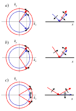
Because of the translational invariance of the system along the -axis, an incident wave , where is the band index, is reflected conserving the -component of the momentum, . The continuity of the wavefunction at the edge requires , where is the total wavefunction. Since two states on the same band with the same have different spin orientations, the boundary condition can only be satisfied if the reflected wave is a linear combination of the two modes and as schematically shown in Figs. 1a and 1b. This superposition of plane waves with different spin generates oscillations of the spin density. This interference effect have interesting properties that manifest more clearly in narrow wires (see next Section).
For the geometry we are considering here (or for wide samples), it is more convenient to analyze first the case of large incident angles. It is clear from Fig.1c that for , there are no propagating modes in the ‘’ band. However, for those values of , the Schödringer equation admittes an evanescent wave solution given by
| (6) |
where
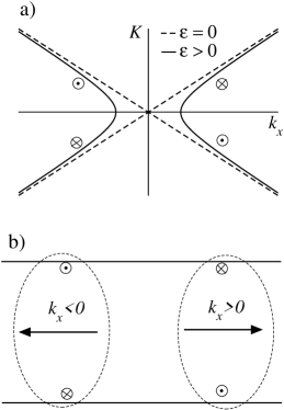
| (7) |
is a normalization constant and . A generic energy surface in the - space is shown in Fig.2. While in bulk this solution does not have any physical meaning, in the presence of a surface it must be included in order to satisfy the boundary condition. The total wavefunction is then a linear superposition of , and . The evanescent modes have two interesting properties which are key ingredients in leading to CISP in wide samples—the solutions for smaller incident angles share some of those properties, as we discuss below, but are less obvious. First, we notice that the evanescent modes have an explicit spin component in the -direction. This is clear from the fact that
| (8) |
Moreover, the sign of the spin projection depends only on the sign of and . Since the sign of is fixed by the condition that the wavefunction remains finite for ( in our case), the sign of the spin projection is giving only by the sign of . Then, electrons with have spin ‘up’ () and those with have spin ‘down’ (). Note that for the evanescent states are fully polarized, for and for and that they are the only states available since . It is worth mentioning that in the case of a wide but finite sample, the solution with dominates at the lower edge while the one with does it at the upper edge. Then, for a given state (value of ) the spin projection have opposite signs in opposites sides of the sample. This is schematically shown in Fig. 2b. Notably, the above results do not depend on the sign of . This result is consistent with the fact that the effective ‘force’Nikolic et al. (2005c); Shen (2005) acting on a wave package is proportional to .

This simple analysis of the evanescent modes shows that there is an intrinsic asymmetry that arises from the combined effect of the breaking of translational invariance and the intrinsic chirality introduced by the spin-orbit interaction, . This is all what is needed to justify the appearance of CISP at . For higher energies, the states without evanescent modes must be included. Although each of those states do not have a well defined spin component in the -direction (it oscillates as a function of ), the sum of all the states with leads to a non-zero contribution which has the opposite sign that the one corresponding to the evanescent modes (see Fig 4). Despite it is hard to prove analytically that such contribution is non-zero, it is rather straightforward to show that each state has the property that the -component of the spin density changes sign when does it.
In order to calculate the CISP in this ideal geometry, we consider a biased 2DEG where the voltage drops at the contacts (not included in the calculation) so the electric field is zero inside the sample. Then, in the energy interval [], the carriers injected from the left contact, which has the highest chemical potential, occupied only the states with .not (b); Datta (1995) The CISP is then given by
| (9) |
where with . In what follows we calculate in linear response by numerical integration of the Schrödinger equation using finite differences. The advantage of this method is twofold: a) it is not restricted to a square well confining potential; b) it can be easily generalized to include the contacts (see next section). All quantities presented below are obtained from the one particle propagators which are calculated using a continues fraction method (see Ref.[Usaj and Balseiro, 2004] for details).
Figure 3 shows for different values of and for meVnm. The insets correspond to the same results convoluted with a Gaussian. It is clear from the figures that the contribution from the evanescent modes is large at low energies and that the CISP goes to zero when the energy is increased.
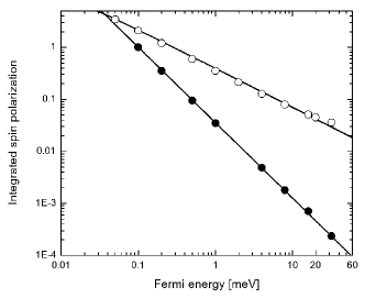
The decay of the CISP with energy is shown in Fig. 4 where we plotted the integrated spin polarization, defined as
| (10) |
as a function of . Both, the total integrated spin polarization (, solid dots) and the one coming from the evanescent modes (, open dots) are shown. Clearly, the decay is well described by a power law. The fact that is smaller than indicates that the spin polarization of the evanescent modes is opposite in sign to the rest of the modes. The decay of can be fitted very well as where is a normalization constant.Usaj and Balseiro (2005)
II.2 Wide wires
The case of a wide but finite sample can be analyzed in a very similar way. The confinement potential is now given by
| (11) |
where is the width of the wire. The only difference here is that a second boundary condition must be imposed, namely . It is clear from Fig. 1 that for a given energy, the four states having the same are mixed. Here again the evanescent modes must be included when (in this case, both solutions with and are required). Figure 5 shows the CISP as a function of the width of the sample. Notice the magnitude of the effect, when averaged over a fixed area, is reduced as the sample becomes wider and that the CISP is more localized at the sample’s edge. Besides the oscillating pattern on the scale of the Fermi wavelength, there is a longer modulation set by the SO coupling, , which is independent of the system’s size.

So far, we have shown that CISP is possible in clean systems with SO coupling due to the special properties of the electron scattering at the sample’s edge. In very wide samples, the effect is essentially confined to a region of order near the edges and its magnitude decay as the Fermi energy increases. As the sample becomes narrower, however, multiple scattering at the edges leads to a different profile for the CISP. It is important to emphasize that there is no conceptual difference between both cases and that the picture described so far is the basic physics underlying the mesoscopic SHE described in Refs. [Nikolic et al., 2005a, d; Yao and Yang, 2005; Usaj and Balseiro, 2005].
III Spin polarization in narrow samples
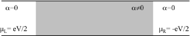
Let us now discuss the CISP in finite samples. In order to do that, we explicitly include the leads in our calculation. For simplicity, we consider leads with the same microscopic parameters than the sample except for the SO coupling parameter which is taken to be zero inside the leads. Since the SO parameter has a spacial variation at the sample-lead interfaces, which is assumed to be only in the -direction, the Hamiltonian includes a term proportional to .not (c) As mentioned before, to be able to describe systems of arbitrary shape, and in order to include the leads, it is convenient to reduce the continuum effective mass model to a tight binding model
| (12) | |||||
where creates an electron at site with spin and energy , for neighboring sites and is the lattice parameter. The SO couplings are defined as follow: deep inside the sample, and at the sample-lead interface and otherwise. The summation is carried out on a square lattice where the coordinate of site is with and the unit lattice vectors in the and directions, respectively. Unless otherwise mentioned, we use a smooth function to turn on the SO coupling in order to avoid stron g reflections at the sample-lead interfaces.
When a voltage bias is applied between the leads, an electric current flows through the sample. In this stationary but out of equilibrium state, the SO coupling generates a pattern of local spin polarization. Within the Keldysh formalism, the spin pattern is given byMahan (2000); Nikolic et al. (2005a)
| (13) |
where the trace is taken on the spin variables, with are the Pauli matrices and the lesser Green function is a matrix with elements . In what follow we consider small bias voltages and linearize Eq. (13). The Fourier transform of the lesser Green function is given byJauho (1996); Pastawski (1992)
where and are the retarded and advanced Green functions, respectively, and are the self-energies due to the left and right leads, is the Fermi function and with . The local spin polarization in the zero temperature limit and in the absence of an external magnetic field, is then given by
| (15) |
In what follows we use this expression to evaluate the CISP in different geometries.
III.1 Quantum wires
We consider a two-terminal wire as shown in Fig. 6. For the case of symmetric samples, as the one considerer here, all components of the CISP have a well defined symmetry,
| (16) |
where is the spatial coordinate measured from the sample’s center. Moreover, a -rotation of the system along the -axis gives
where the last equality is due to the symmetry of the Hamiltonian, . Similarly a -rotation along the -axis gives
In linear response, these relations imply that,Yao and Yang (2005)
| (19) |
Note that in systems with translational invariance (or in the case of very large samples), the first equation implies , in agreement with the results of the previous section. Any deviations from the symmetry relations shown in Eq. (19), such as a larger spin polarization near the drain contact, can only arise from non-linearities.Nikolic et al. (2005a)
The transverse structure of the different components of is determined by three characteristic lengths: the Fermi wavelength , the SO length and the sample width . For wide samples () it has been shown in the previous section that the CISP presents transverse oscillations with the two characteristic lengths and . The resulting structure shows a beating of the two lengths with a net spin polarization at the sample border.
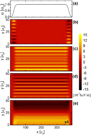
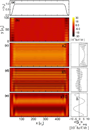
Results for narrow samples () are shown in Figs. 7 and 8. All the symmetries mentioned above are apparent in the figures. The profile of the Rashba parameter is shown in the top panels. We notice that: (i) (panel (b)) is zero away from the sample-lead interfaces; (ii) is the largest spin component having a defined sign throughout the channel; and (iii) (panel (d)) oscillates with a dominant sign on each side of the wire. To emphasize the later behavior, we made a convolution of with a Gaussian with an rms of three lattice parameters (). The convoluted spin density (panel (e)) clearly shows the spin polarization with opposite signs at the two sides of the wire. As oppose to the wide sample case, however, the transverse profile shows strong oscillations whose magnitude is comparable with the value of the magnetization close to the edges.
It is interesting to note that the penetration of the -component inside the sample depends on the sample-lead interface. When the Rashba parameter is turned on abruptly, the interference induced by the now strong scattering at both interfaces leads to oscillations of along the -axis—such oscillating pattern is also visible on the other two spin components. This is shown in Fig. 9. Another important feature is that in long samples ( ), and when is turned one adiabatically, the finite size results away from the interface are the same as those obtained in the previous section for infinite long systems.
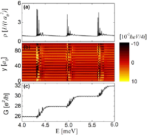
The CISP is dominated by the channel that contributes the most to the density of states (DOS) at the Fermi level. This is shown in Fig. 10 where the transverse structure of is plotted as a function of for a fixed value of . Clearly the -component of the CISP is sensitive to the position of the Fermi energy and the number of oscillations depends on the wavelength of the corresponding transverse mode. In particular, if lies close to the bottom of a channel, the magnetization pattern is strongly modified: its magnitude increases and its sign can change. This behavior suggest that when large voltages are applied to narrow samples, and therefore a wide energy window around is involved, non-linear effects might be important due to the contribution of states at the bottom of each channel. It also shows the sensitivity of the CISP to the geometry while emphasizes the nature of the effect: it arises from the interference of the different spin states which are mixed by the scattering at the interface and the non-equilibrium occupancy of the momentum states.
III.2 ‘T’ and ‘L’ shaped samples
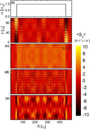
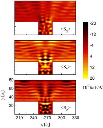
As mentioned in the previous sections, in the case of small samples, both the magnitude and the profile of the CISP relies on the geometry of the system. However, so far we have discussed only the wire geometry. In this section we will discuss two different geometries: a ‘T’ and a ‘L’ shaped sample.
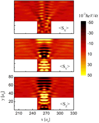
Figures 11 and 12 show the three components of the CISP for the case of a ‘T’ shaped sample: it corresponds to a quantum wire with a open cavity attached to it. The cavity is large enough to originate a (resonant) state which is substantially localized around the cavity. Figure 11 correspond to an arbitrary value of while in Fig. 12 it is tuned to correspond to a resonant state. Notice that all components are different from zero. While in both cases there is some additional polarization in the vicinity of the cavity, the latter case shows a strong enhancement. We note that because the cavity is at the center of the system, some of the symmetry relationships shown in Eq. (19) are still valid. These results suggest that an adequate engineering of the sample geometry might allow to design different profiles for the spin polarization, such as focusing the spin polarization on a given spot, for instance. Notably, the amount of spin polarization is very large—in systems without SO a Zeeman field of T, would be required to achieve a similar polarization density.
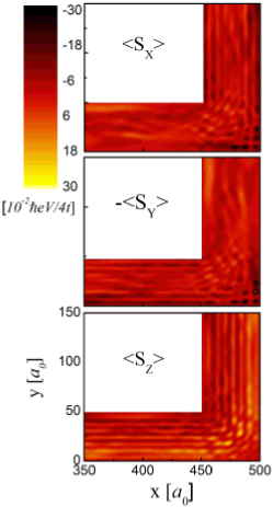
Figure 13 shows the corresponding results for the ‘L’ shaped sample. The presence of the ‘corner’ induces some additional spin polarization as compared to the wire geometry. The symmetry between and in the two ‘legs’ of the ‘L’ is apparent from the figure—to emphasize this, we have plotted instead of . Because of the strong scattering at the corner, the longitudinal spin component does not decay to zero, even far from it. This is similar to the case of an abrupt turn on of the Rashba parameter.
IV Summary and conclusions
We have showed that current induced spin polarization is possible in ballistic 2DEGs. The effect is purely geometrical and arises from the electron scattering at the sample boundary. For this reason, the CISP is strongly dependent on the shape of the sample while some spin components can be very sensitive to the sample-lead interface. In addition, the CISP is quite sensitive to the value of the Fermi energy. This is true in both wide and narrow samples, though for different reasons. In wide samples, the CISP contains two distinct contribution: one comes from the interference of the two components of the scattered wave, which are two bulk Bloch states from different bands, and the other from the evanescent modes that appear at the boundary. Both contributions have different signs and so tend to cancel each other. At low the evanescent modes clearly dominate so there is a large CISP. When the value of is increased, the cancellation between the two contributions is better and the CISP goes to zero. One interesting feature of the CISP for this case is that it does not decay monotonically to zero as one goes from the boundary to the bulk of the sample but oscillates. Then, even on a given side of the sample, the polarization can change its sign. It is worth mentioning that because of this strong decay with , the phenomena described here cannot account for the magnitude of the effect observed in Ref. Sih et al., 2005. In such device, the presence of a strong disorder and an electric field seems to play an important role. One possible explanation, within our intrinsic model, is that disorder might rapidly destroy the phase of the scattered wave without affecting the evanescent states too much, therefore unbalancing the cancellation of the two contributions. In any case, we believe, that the special properties of the scattering at the surface plays a crucial role in originating the CISP in those samples.
The case of narrow systems is a bit different. There, the CISP is dominated by the interference of the waves scattered at both sides of the sample. Because of the strong confinement, the density of states have some structure and then, depending on , only a few states might dominate the CISP. This is more clearly seen when is close to the bottom of a transverse channel or, in the presence of a side cavity, near a resonant state. In this regime the profile of the CISP very much resembles that of a single wavefunction. This opens up the possibility to design different profiles for the CISP by modifying the geometry of the sample.
V Acknowledgments
This work was partially supported by ANPCyT Grants No 13829 and 13476 and Fundación Antorchas, Grant 14169/21. AR and GU acknowledge support from CONICET.
References
- Awschalom et al. (2002) D. Awschalom, N. Samarth, and D. Loss, eds., Semiconductor Spintronics and Quantum Computation (Springer, New York, 2002).
- Dyakonov and Perel (1971) M. I. Dyakonov and V. I. Perel, JETP Lett. 13, 467 (1971), ;Phys. Lett. A 35, 459 (1971).
- Hirsch (1999) J. E. Hirsch, Phys. Rev. Lett. 83, 1834 (1999).
- Murakami et al. (2003) S. Murakami, N. Nagaosa, and S. C. Zhang, Science 301, 1348 (2003).
- Sinova et al. (2004) J. Sinova, D. Culcer, Q. Niu, N. A. Sinitsyn, T. Jungwirth, and A. H. MacDonald, Phys. Rev. Lett. 92, 126603 (2004).
- Kato et al. (2004) Y. K. Kato, R. C. Myers, A. C. Gossard, and D. D. Awshalom, Science 306, 1910 (2004).
- Wunderlich et al. (2005) J. Wunderlich, B. Kaestner, J. Sinova, and T. Jungwirth, Phys. Rev. Lett. 94, 047204 (2005).
- Kato et al. (2005) Y. K. Kato, R. C. Myers, A. C. Gossard, and D. D. Awschalom (2005), cond-mat/0502627 (unpublished).
- Sih et al. (2005) V. Sih, R. C. Myers, Y. K. Kato, W. H. Lau, A. C. Gossard, and D. D. Awschalom (2005), cond-mat/0506704 (unpublished).
- Rashba (2003) E. I. Rashba, Phys. Rev. B 68, 241315(R) (2003).
- Mishchenko and Halperin (2003) E. G. Mishchenko and B. I. Halperin, Phys. Rev. B 68, 045317 (2003).
- Schliemann and Loss (2003) J. Schliemann and D. Loss, Phys. Rev. B 68, 165311 (2003).
- Inoue et al. (2003) J. I. Inoue, G. E. W. Bauer, and L. W. Molenkamp, Phys. Rev. B 67, 033104 (2003).
- Hankiewicz et al. (2004) E. M. Hankiewicz, L. W. Molenkamp, T. Jungwirth, and J. Sinova, Phys. Rev. B 70, 241301(R)) (2004).
- Inoue et al. (2004) J. Inoue, G. E. W. Bauer, and L. W. Molenkamp, Phys. Rev. B 70, 041303(R) (2004).
- Mishchenko et al. (2004) E. G. Mishchenko, A. V. Shytov, and B. I. Halperin, Phys. Rev. Lett. 93, 226602 (2004).
- Khaetskii (2004) A. Khaetskii (2004), cond-mat/0408136.
- Rashba (2004a) E. I. Rashba, Phys. Rev. B 70, 201309(R) (2004a).
- Culcer et al. (2004) D. Culcer, J. Sinova, N. A. Sinitsyn, T. Jungwirth, A. H. MacDonald, and Q. Niu, Phys. Rev. Lett. 93, 046602 (2004).
- Governale and Zülicke (2004) M. Governale and U. Zülicke, Solid State Comm. 132, 581 (2004).
- Rashba (2004b) E. I. Rashba, Phys. Rev. B 70, 161201(R) (2004b).
- Usaj and Balseiro (2005) G. Usaj and C. A. Balseiro, Europhys. Lett. 72, 621 (2005).
- Nikolic et al. (2005a) B. K. Nikolic, S. Souma, L. P. Zarbo, and J. Sinova, Phys. Rev. Lett. 95, 046601 (2005a).
- Nikolic et al. (2005b) B. K. Nikolic, L. P. Zarbo, and S. Souma, Phys. Rev. B 72, 075361 (2005b).
- Sheng et al. (2005) L. Sheng, D. N. Sheng, and C. S. Ting, Phys. Rev. Lett. 94, 016602 (2005).
- Nikolic et al. (2005c) B. K. Nikolic, L. P. Zarbo, and S. Welack, Phys. Rev. B 72, 075335 (2005c).
- Chalaev and Loss (2005) O. Chalaev and D. Loss, Phys. Rev. B 71, 245318 (2005).
- Bernevig and Zhang (2005) B. A. Bernevig and S.-C. Zhang, Phys. Rev. Lett. 95, 016801 (2005).
- Raimondi and Schwab (2005) R. Raimondi and P. Schwab, Phys. Rev. B 71, 033311 (2005).
- Mal’shukov and Chao (2005) A. G. Mal’shukov and K. A. Chao, Phys. Rev. B 71, 121308(R) (2005).
- Engel et al. (2005) H.-A. Engel, B. I. Halperin, and E. I. Rashba, Phys. Rev. Lett. 95, 166605 (2005).
- Erlingsson and Loss (2005) S. I. Erlingsson and D. Loss, Phys. Rev. B 72, 121310(R) (2005).
- Nomura et al. (2005a) K. Nomura, J. Sinova, T. Jungwirth, Q. Niu, and A. H. MacDonald, Phys. Rev. B 71, 041304(R) (2005a).
- Adagideli and Bauer (2005) I. Adagideli and G. E. Bauer (2005), cond-mat/0506531.
- Nomura et al. (2005b) K. Nomura, J. Wunderlich, J. Sinova, B. Kaestner, A. MacDonald, and T. Jungwirth (2005b), cond-mat/0508532 (unpublished).
- Nikolic et al. (2005d) B. K. Nikolic, L. P. Zarbo, and S. Souma (2005d), cond-mat/0506588.
- Tse et al. (2005) W.-K. Tse, , J. Fabian, I. Zutic, and S. D. Sarma (2005), cond-mat/0508076.
- Lozano and Sanchez (2005) G. S. Lozano and M. J. Sanchez, Phys. Rev. B 72, 205315 (2005).
- Edelstein (1990) V. M. Edelstein, Solid State Comm. 73, 233 (1990).
- Winkler (2003) R. Winkler, Spin-orbit coupling effects in two-dimensional electron and hole systems (Springer-Verlag, 2003).
- not (a) We use the term ’polarization’ instead of ’accumulation’ to emphasize the fact that the effect discussed here does not result from the flow of a spin current that ’accumulate’ spins at the boundary but rather from the difference in the occupation of the right-moving () and left-moving () states.
- Shen (2005) S.-Q. Shen, Phys. Rev. Lett. 95, 187203 (2005).
- Schliemann et al. (2005) J. Schliemann, D. Loss, and R. M. Westervelt, Physical Review Letters 94, 206801 (2005).
- Jauho (1996) H. Jauho, Quantum kinetics in transport and optics of semiconductors (Springer, 1996).
- Pastawski (1992) H. M. Pastawski, Phys. Rev. B 46, 4053 (1992).
- Khodas et al. (2004) M. Khodas, A. Shekhter, and A. Finkel’stein, Phys. Rev. Lett. 92, 086602 (2004).
- Ramaglia et al. (2004) V. M. Ramaglia, D. Bercioux, V. Cataudella, G. D. Filippis, and C. A. Perroni, J. Phys.:Condens. Matter 16, 9143 (2004).
- Chen et al. (2005) H. Chen, J. J. Heremans, J. A. Peters, A. O. Govorov, N. Goel, S. J. Chung, and M. B. Santos, Appl. Phys. Lett. 86, 032113 (2005).
- Rashba (1960) E. I. Rashba, Sov. Phys. Solid State 2, 1109 (1960).
- Bychkov and Rashba (1984) Y. A. Bychkov and E. I. Rashba, JETP Letters 39, 78 (1984).
- not (b) We only consider the case .
- Datta (1995) S. Datta, Electronic transport in mesoscopic systems (Cambridge Univ. Press, 1995).
- Usaj and Balseiro (2004) G. Usaj and C. A. Balseiro, Phys. Rev. B 70, 041301(R) (2004).
- Yao and Yang (2005) J. Yao and Z. Yang (2005), cond-mat/0507025.
- not (c) In the tight-binding version of the Hamiltonian, this term translates in a position dependent spin-orbit coupling (see Eq. 12).
- Mahan (2000) G. D. Mahan, Many-particle physics (Kluwer Academic/Plenum Publishers, 2000), 3rd ed.