Multiple charging of InAs/GaAs quantum dots by electrons or holes: addition energies and ground-state configurations
Abstract
Atomistic pseudopotential plus configuration interaction calculations of the energy needed to charge dots by either electrons or holes are described, and contrasted with the widely used, but highly simplified two-dimensional parabolic effective mass approximation (2D-EMA). Substantial discrepancies are found, especially for holes, regarding the stable electronic configuration and filling sequence which defies both Hund’s rule and the Aufbau principle.
pacs:
73.21.La, 73.23.Hk 73.63.KvI Introduction
One of the most spectacular aspects of quantum-dot physics is that dots can be controllably charged by either electrons or holes and that one can measure, for each of the many charged-states, both the electronic spectrum and the charging energies. This is afforded either by injecting from a tip of a scanning tunneling microscope, Banin et al. (1999) or by various gate structures. Kastner (1993); Tarucha et al. (1996); Drexler et al. (1994); Fricke et al. (1996); Miller et al. (1997); Kouwenhoven et al. (1997); Bödefeld et al. (1999); Regelman et al. (2001); Warburton et al. (2000); Reuter et al. (2005) Since the energy scale of both single-particle levels and Coulomb interactions in quantum dots (QDs) ( - Ry) are a few order of magnitudes smaller than those of the real atoms ( 1 Ry), dots can be loaded by as many as six Drexler et al. (1994) to ten Banin et al. (1998) electrons in colloidal Banin et al. (1998) and self-assembled Drexler et al. (1994); Bödefeld et al. (1999); Regelman et al. (2001) dots having confining dimension of 50 Å, and up to hundreds of electrons in larger 500 Å electrostatically confined dots. Tarucha et al. (1996); Kouwenhoven et al. (1997); Kastner (1993) The “charging energy” is the energy needed to add a carrier to the dot that is already loaded by carriers,
| (1) |
where is the correlated, many-body total energy of the ground state of the -particle dot. The “addition energy” (analogous to the difference between ionization potential and electron affinity) indicates how much more energy is needed to add the th carrier compared to the energy needed to add the th carrier:
| (2) | |||||
The typical electron addition energies for electrostatic dots, Tarucha et al. (1996); Kouwenhoven et al. (1997); Kastner (1993) are about 1 - 8 meV, and the stable spin-configuration follows the rules of atomic physics; that is, the s, p, d, … shells are occupied in successive order with no holes left behind (Aufbau principle) and with maximum spinTarucha et al. (1996) (Hund’s rule). Recently, it became possible to load and measure electrons Drexler et al. (1994); Bödefeld et al. (1999) and holes Bödefeld et al. (1999); Reuter et al. (2004, 2005) into much smaller, epitaxially grown self-assembled dots of InGaAs/GaAs, where electron addition energies are about 10 - 60 meV, Drexler et al. (1994); Bödefeld et al. (1999) and hole addition energies are between 10 - 30 meV.Reuter et al. (2004, 2005) More interestingly, while electrons still follow the Aufbau principle, recent hole charging experiment Reuter et al. (2005) show that holes have unusual charging patterns that defy the Aufbau principle and Hund’s rule.
Despite the importance of the dot charging problem and the great success achieved in experimentally recording the charging spectra, the theoretical understanding of charging and addition energies is still preliminary. Most theoretical works in the area were based on particle-in-a-potential model, Jacak et al. (1998); Wojs and Hawrylak (1996); Warburton et al. (1998); Rontani et al. (1998) neglecting interband (e.g., -) coupling, intervally (--) coupling effect, and the true atomistic symmetry (e.g., for lens of zincblende material) which is lower than the shape symmetry. The most often used potential in such approaches is the 2-dimensional (2D) parabolic form, in which all of the above noted electronic structure effects are replaced by an effective mass approximation (EMA). In this 2D-EMA model,Jacak et al. (1998); Warburton et al. (1998) the single particle levels have equal spacing, which equals a harmonic oscillator frequence . Because of the simplicity of the model, all the Coulomb integrals can be related analytically Warburton et al. (1998) to a single orbital Coulomb energy , and therefore the addition energies are determined entirely by and . Although the 2D-EMA model can be attractive because of its algebraic simplicity, and availability of fitting parameters, actual self-assembled dots are significantly different from the description of EMA model, manifesting inter-band coupling and inter-valley coupling, strain effects, low atomistic symmetry, as well as specific band offset profiles, all neglected by the 2D-EMA. It indeed has been recently shown He et al. that hole ground state configurations predicted by the 2D-EMA model are qualitatively different from those measured by hole charging experiments.Reuter et al. (2004, 2005)
An atomistic pseudopotential description of electronic structure effects can be used instead of 2D-EMA to calculate charging energies. Williamson et al. (2000); Bester and Zunger (2003, 2005); Franceschetti and Zunger (2000); He et al. Here, we show that such an atomistic theory correctly reproduces the many-particle configurations as well as addition spectra for carriers in self-assembled quantum dots. We study systematically the electronic structure of self-assembled InGaAs/GaAs quantum dots, provide detailed information on the electron and hole single-particle spectrum, many-particle charging and addition spectrum, as well as ground state configurations using single-particle pseudo-potential and many-particle configuration interaction (CI) methods.
The rest of the paper is arranged as follows. In Sec. II, we introduce the basic concepts of charging and addition energies, and show how to calculate these quantities in the single-particle pseudopotential plus many-particle CI scheme. In Sec. III, we give detailed results calculated from pseudopotential-CI scheme the single-particle levels, Coulomb integrals and the ground state configurations as well as the addition energies. We contrast these results with 2D-EMA model. We summarize in Sec. IV.
II Theory of dot charging and addition energies
II.1 General equation for dot charging in the configuration-interaction approach
The calculation of the total-energy of -particle dot requires obtaining first the single-particle states from an effective Schrödinger equation, and then the many-particle state from a many-particle treatment. The first step is formulated as,
| (3) |
where is the external (“bare”) potential experienced by the electrons or holes, and is the screening response. The single-particle orbital and energies are used in the second step to construct the many-particle wave functions and energies from,
| (4) |
where, the many-body Hamiltonian is,
| (5) | |||||
and,
| (6) |
are the screened Coulomb and exchange integrals. In the above Eqs. (5) and (6), “” is a pseudospin index, i.e., an index of Kramers degenerate states, while “” is the intrinsic electronic spin. For electrons in InAs/GaAs QDs, the spin-orbit interactions is extremely small and can be neglected. In this case, the pseudospin and intrinsic electronic spin are equivalent. However, for holes, which have a mixture of heavy-, (H) light-hole (LH) and split-off character, an eigenstate of has both and components. The -particle wave functions can be solved using e.g. configuration interaction (CI) method, Szabo and Ostlund (1996) by expanding the -electron wave function in a set of Slater determinants, , where creates an electron in the state . The -th many-particle wave function is then the linear combination of the determinants,
| (7) |
Once is known, we can then calculate the corresponding total energies for the ground states as well as excited states using Eq. (4). Once we solve the CI problem, we get the order of total CI energy for various holes or electron configurations, so we can see if Hund’s rule or the Aufbau principle or spin-blockade occurs. For example, Hund’s rule states that degenerate single-particle levels are occupied with maximum number of unpaired electrons, while the Aufbau principle states, non-degenerate single-particle levels are occupied in order of increasing single-particle energy.
We construct all possible Slater determinants corresponding to electrons or holes [i.e., we ignore the excitonic (electron+hole) excitations], using only the bound states of the dots, (i.e., we neglect all continuum states). The underlying electrons that are not considered explicitly by this approach are represented by the dielectric screening function in Eq. (6).
II.2 The Hartree-Fock equations for charging and addition energies
The addition energies at CI level can be written as the Hartree-Fock (HF) addition energies plus the correlations, i.e.,
| (8) |
where is the correlation energy correction to the addition energy calculated in HF. Since the HF equations are used by many experimentalists to deduce Coulomb energies,Bödefeld et al. (1999); Reuter et al. (2005); Tarucha et al. (1996) we review it here. In the Hartree-Fock approximation, where the effect of correlations is neglected but the direct Coulomb and exchange interactions are retained, simple expressions can be derived for the addition energies. The total energy of electrons is simply,
| (9) |
where, is the single-particle level index of all occupied states, and is the corresponding single-particle energy. The and in Eq. (9) are Coulomb and exchange integrals, respectively. Since the spin index “” is not an actual electronic spin, but rather an index for two Kramers degenerate states, in principle the exchange integrals are not simply diagonal in , , as has been widely used in the dot charging literature. Warburton et al. (1998); Tarucha et al. (1996); Wojs and Hawrylak (1996); Reuter et al. (2005) However, adopting the literature approximation, = and considering the and two orbitals, and assuming the particle filling order follows Hund’s rule, as shown in Fig.1, the total energies for =1, 2, 3, 4 electrons in the Hartree-Fock approximation are
| (10) | |||||
We can then readily calculate the charging energies Eq. (1) in this approximation,
| (11) |
Similarly, we can calculate the addition energies Eq. (2) as follows,
| (12) | |||||
From above equations, we see that to predict for the first two cases (=3), we need to know 4 parameters (, , , ), but for =6, we need to know 9 parameters. Because of the large number of parameters needed, the analysis of charging effects in the literature resort to additional approximations aimed at reducing the number of parameters using simplified effective mass models. Equations (12) are going to be used below to contrast the charging spectra deduced from simplified literature models vs. our more complete treatment.

II.3 Atomistic treatment of the single-particle problem
The most general treatment of the single-particle problem of Eq.(3) describes both and atomistically, much in the same way as molecules are treated quantum-mechanically. In this description is a superposition of the ionic potential of individual atoms of type at lattice site ,
| (13) |
and is in an all-electron (core+valence) treatment (where is the atomic number) or in the pseudopotential (valence-only) scheme (where is the ionic pseudopotential. The potential naturally contains the correct point-group symmetry of the object, through the atomic position vectors , and includes atomic relaxation if appropriate (again, through the atomic positions), as well as chemical inhomogeneity (alloying) or surface-passivation effect. The screening response of Eq. (3) is in general a functional of the density-matrix and can be described e.g. via Hartree-Fock or the density functional theory, both requiring a self-consistent (iterative) solution to Eq. (3). These approaches are currently limited to small dots, relative to the 103 - 105 atom dots which charging experiments exist. Furthermore, LDA suffer from the famous “LDA error”, whereby the band gap and effective masses are badly underestimated. Higher-order method such as GW approximation or time-depend DFT have yet to demonstrate applicability to large dots for which high-quality experiments exit.
An approximation to the screening , which allows calculation on large dots, and fixes the LDA error, is provided by the “screened pseudopotential approach”, where it is assumed that can be described as a superposition of screening potentials of the individual atoms, and lumping together to yield a screened atomic pseudopotential , such that,
| (14) |
Here, is determined semi-empirically. Unlike the classic empirical pseudopotential method, Cohen and Bergstresser (1966) which fitted only to eigenvalues, here we require that when Eq. (3) is applied to the underlying bulk periodic solids containing atom , reproduce the measured band energies, effective-mass tensors, deformation potentials, and the single-particle wave functions have a large overlap with the corresponding LDA wave functions.Wang and Zunger (1995); Fu et al. (1997a) In Eq. (14), a nonlocal potential is also added to the total potential to represent the spin-orbit interaction. In our approach, the potential of an As atom depends on the number of Ga and In atoms around it as
| (15) |
where is the number of Ga atoms around the As atom. In this atomistic approach, one assume that is transferable to different environments. Note that a fixed is a good approximation if the dot has no free surfaces (as is the case in self-assembled dots, where only a strained interface between chemically-similar materials is present). For surface atoms in free-standing dots, a separate is fitted Fu et al. (1997b) to LDA surface calculations. For InAs/GaAs dots, we use the pseudopotentials of Ref.Williamson et al., 2000. These pseudopotentials have been tested not only for the InAs and GaAs binaries, but also for alloys and superlattices of the corresponding ternaries. Williamson et al. (2000)
Once is known, one can solve Eq. (3) for the bulk solid, quantum wells superlattices, quantum-wires or quantum dots by adopting a supercell approach where the respective objects are placed. In our case, Eq. (3) is solved using the “linear combination of Bloch bands” (LCBB) method,Wang and Zunger (1999) where the wave functions are expanded as,
| (16) |
In the above equation, are the bulk Bloch orbitals of band index and wave vector of material (= InAs, GaAs), strained uniformly to strain . The inclusion of stain-dependent basis functions improves their variational flexibility. We use for the (unstrained) GaAs matrix material, and an average value from VFF for the strained dot material (InAs). For the InAs/GaAs system, we use (including spin) for electron states on a 6616 k-mesh. Note that the potential contain full strain effects through the use of relaxed atomic positions, in addition to the explicit strain Williamson et al. (2000) and alloy composition Magri and Zunger (2002) dependence.
In the atomistic approach to the single-particle problem, one includes (i) multi-band coupling [different in Eq. (4)]; (ii) inter-valley coupling [different bulk -points in Eq. (4)]; (iii) spin-orbit coupling [ in Eq. (14)]; (iv) the proper strain profile [by relaxing in Eq. (14) to minimize strain]; (v) realistic chemical profile [distributing the species as in a random alloy, Williamson et al. (2000) or interdiffused interfaces Magri and Zunger (2002)]. The ensuing single-particle orbitals transform like the representations of the point-group created by the ionic positions. These underlying atomistic structures could break the symmetry represented by the macroscopic shape of the quantum dots. For example, a lens-shaped dot has a macroscopic cylindrical symmetry with [110] and [10] being equivalent, but if the dot is made of a zincblende material, the real symmetry is , where, [110] and [10] are not equivalent. Yet the continuum models do not “see” the atomistic symmetry (the “farsightedness effect”Zunger (2002)). Therefore, as discussed in Ref. He et al., 2004, in reality the atomistic wave function need not to be simple “pure” -like or -like. As a result, the Coulomb energy and exchange energy obtained with atomistic single-particle orbital do not have simple relationships Warburton et al. (1998) as predicted by continuum 2D-EMA model. The deviations of the atomistic calculated s from the simplified 2D-EMA ones are going to lead to new physical behavior (e.g., new ground state symmetry of the many-particle state), as illustrated below.
II.4 Continuum treatment of the single-particle problem: EMA
It is sometimes customary Warburton et al. (1998); Reuter et al. (2005); Tarucha et al. (1996); Dekel et al. (2000) to avoid an atomistic description of the single-particle problem in favor of a single-band particle-in-a-box model. In this approach, one sets =0 and replaces of Eq. (3) by a pure external potential, describing the macroscopic shape of the object, e.g., a box represents a quantum well, or a sphere with finite or infinite barriers represents a quantum dot. Jacak et al. (1998); Bimberg et al. (1999); Warburton et al. (1998) In some cases, this is calculated “realistically” from a combination of band offset, the gate potential and the ionized impurities,Fonseca et al. (1998); Bednarek et al. (2003) but it is treated nevertheless as a macroscopic external field. Under this approximation, simple results can be obtained for cylindrical QDs, where the angular momentum and are good quantum numbers. The electron (hole) single-particle levels have well defined shell structures, with non-degenerate shell, two-fold degenerate shell, and three-fold degenerate shell, etc. Furthermore, for parabolic confining potentials, the single-particle levels have equal spacing between two adjacent shells, e.g. =. Another reason for the attractiveness of the single-band particle-in-a-box approach to the single-particle problem [Eq.(3)], is that the many-particle problem [Eq.(5)] becomes simple. For example, the quantum Monte Carlo (QMC) approach is currently applied only within the single-band particle-in-a-box approach for such large objects as self-assembled quantum dots. Shumway et al. (2001) In a 2D-EMA model all the Coulomb integrals needed for charging and addition energy can be all related to Warburton et al. (1998) ,
| (17) |
For example, , . Therefore the charging/addition energies and ground state configurations are totally determined by and the single-particle energy spacing .
However, real self-assembled quantum dots grown via the Stranski-Krastanov techniques, are not well-described by the single-band particle-in-a-box approaches, despite the great popularity of such approaches in the experimental literatures. Warburton et al. (1998); Reuter et al. (2005); Dekel et al. (2000); Wojs and Hawrylak (1996) The model contains significant quantitative errors Wang et al. (2000) and also qualitative errors, whereby cylindrically symmetric dots are deemed to have, by symmetry, no fine-structure splitting, no polarization anisotropy, and no splitting of levels and levels, all being a manifestation of the “farsightedness effect”.Zunger (2002)
III results
| Height (nm) | 2.5 | 3.5 | 2.5 | 3.5 | 3.5 | 3.5 | 3.5 | 2.5 | 3.5 |
| Base (nm) | 20 | 20 | 25 | 25 | 25 | 25 | 25 | 27.5 | 27.5 |
| Ga comp. | 0 | 0 | 0 | 0 | 0.15 | 0.3 | 0.5 | 0 | 0 |
| 77.0 | 72.0 | 60.8 | 57.0 | 51.5 | 44.2 | 33.2 | 54.9 | 51.0 | |
| 79.7 | 73.6 | 64.0 | 58.7 | 50.7 | 43.2 | 18.8 | 57.9 | 52.3 | |
| 2.5 | 3.7 | 1.6 | 2.1 | 2.5 | 1.2 | 0.8 | 1.1 | 2.0 | |
| 3.1 | 2.8 | 1.2 | 1.4 | 4.0 | 1.3 | 4.1 | 0.8 | 1.0 | |
| 17.8 | 10.4 | 17.4 | 11.3 | 13.1 | 13.7 | 12.8 | 17.0 | 11.3 | |
| 10.9 | 11.3 | 7.1 | 9.5 | 7.1 | 5.0 | 3.3 | 5.8 | 7.9 | |
| 4.5 | 3.4 | 8.3 | 2.4 | 6.4 | 8.6 | 9.4 | 9.4 | 3.9 | |
| 1080 | 1035 | 1042 | 996 | 1095 | 1188 | 1297 | 1028 | 981 |
Using the pseudopotential approach for single-particle and configuration interaction approach for the many-particle step, we studied the electron or hole addition energy spectrum up to 6 carriers in lens-shaped InAs dots embedded in a GaAs matrix. We study dots of three different base size, = 20 nm, 25 nm and 27.5 nm, and for each base size, two heights, =2.5 nm and 3.5 nm. To study the alloy effects, we also calculated the addition spectrum for alloy dots In1-xGaxAs/GaAs of /=3.5/25 nm dots, with Ga composition =0, 0.15, 0.3 and 0.5. In this section, we give detailed results of the single particle energy levels and Coulomb integrals, and the addition energy as well as ground state configurations. We also compare the results with what can be expected from 2D-EMA model.
III.1 Single-particle level spacing: Atomistic vs. 2D-EMA description

III.1.1 Electron levels
We depict in Fig. 2 the calculated energy-level diagram of a pure lens-shaped InAs/GaAs quantum dot, with height =2.5 nm and base =20 nm. Figure 2 shows that the electron confinement energy is 230 mev, somewhat larger than the hole confinement energy (190 meV). The levels are split as are the levels, even though the dot has macroscopic cylindrical symmetry (see below).
The pseudopotential calculated electron single-particle energy spacings are summarized in Table 1 for QDs of different heights, bases, and alloy compositions. Table 1 gives the fundamental exciton energy calculated from CI approach for each dot. These exciton energies are between 980 meV - 1080 meV for pure InAs/GaAs dots, and can be as large as 1297 meV for In1-xGaxAs/GaAs alloy dots. This range agrees very well with experimental results for these classes of dots, ranging from 990 meV to 1300 meV. Schmidt et al. (1996, 1998); Bödefeld et al. (1999); Reuter et al. (2005)
(a) - and - energy spacing: From Table 1, we see that for electrons in the lens-shaped dot, the - energy level spacing and - energy level spacing are nearly equal, as assumed by the 2D harmonic model. The energy spacing and range from 50 - 80 meV (Fig. 2), depending on the dot geometries. The electron energy spacings decrease with increasing QD base sizes. The electron energy spacing of alloy dots are much smaller than those in pure InAs/GaAs QDs, because of reduced confinement. For Ga rich dots (=0.3 - 0.5), the single-particle energy level spacings range from 30 - 45 meV. These values agree with the infrared absorption measurements Drexler et al. (1994); Fricke et al. (1996) of intra-band transitions of alloy InGaAs QDs, which give 41 - 45 meV. When the Ga composition reaches =0.5, the - energy level spacing becomes significantly different from the - energy level spacing , thus deviating from harmonic potential approximation.
(b) Shell definition: Figure 2 shows that the energy levels of electrons in a lens-shaped dot have well defined , shell structure. However, while effective mass and models predict degenerate and levels, for cylindrically-symmetric (e.g. lens-shaped) QDs, atomistic calculations show that even in perfect lens-shaped dots, the - and - levels are split by 2 - 4 meV (Fig. 2) due to the actual symmetry. We denote the two levels as and , and similarly, the three levels as , and , in increasing order of energy. The results listed in Table 1 show that and are very sensitive to the aspect ratio of the dots while not being very sensitive to the alloy compositions. Figure 3 depicts vs. dot heights [Fig.3(a)] and bases sizes [Fig.3(b)]. In general, we see that increases with increasing dot height, and it decreases with increasing dot base size.
III.1.2 Hole levels
In contrast to electrons, hole single-particle levels (Table 1) display a much more complicated behavior that is totally beyond the EMA description.
(a) - spacing: As one can see from Table 1, the hole - energy spacing ranges from 10 - 18 meV for dots of sizes we studied. These energy spacings are considerably smaller than those of electrons. The first confined hole state is found to be about 190 meV above the VBM of bulk GaAs, for the pure, =2.5/20 nm dot (Fig. 2). Unlike the case for electrons, the energy spacing between hole and levels depends strongly on the height of the dots, foo (a) while being relatively insensitive to the base size of the dots.
(b) Shell definition: The well-defined , , shell-structure for electrons does not exist for holes (Fig. 2), as the - and -- splitting are much larger than those for electrons.foo (b) The hole -level splittings are also shown in Fig. 3 for different dot heights [Fig.3(a) ] and bases sizes [Fig.3(b)]. For the smallest dots, / = 2.5/25 nm, the splitting is about 11 meV (Table 1), more than 3 times the value for electrons. This splitting is about half of the hole - energy spacing. Note that the pseudopotential calculated - splitting is much lager than 1.3 meV given by the method (which includes piezoelectric effect). Sheng et al. (2005) For taller dots, the - splittings are even larger. As a consequence, the levels are energetically very close to the levels, leading, as we will see below, to a nontrivial charging pattern that breaks Hund’s rule and the Afubau principle. He et al.
(c) Wave function characters: An analysis of the wave function show that these levels have somewhat mixed , or characters. For example, for a lens-shaped InAs/GaAs QD of height=3.5 nm and base=25 nm, the “ level” has 92% character, and the two “ levels”, and , have 86% character respectively (see Table II of Ref. He et al., 2004). Therefore, we can still label the single-particle levels as , , , etc. These single-particle levels, , and , do not have pure HH character either, being instead 91%, 86%, and 92% HH-like respectively. As the aspect ratio height/base increases, the mixture of angular momentum and HH and LH characters becomes stronger. For example, as shown in Ref. Narvaez et al., 2005, for a InGaAs/GaAs alloy dot, with 25.2 nm in base and 2 nm in height, level has 90% character, while both and levels have 84% character. When the height of the dot increases to 7.5 nm (with fixed base size), the leading angular momentum characters for these three levels are 84% , 78% and 75 % respectively. Similarly, for the flat dot (2 nm in height), the mixture of LH state character is about 4 - 9 %, but increases to 11 - 17 % for the tall dot (7.5 nm in height).
| 2D-EMA | Atomistic | |||||
| Height (nm) | 1.5 | 2.5 | 3.5 | 5.0 | 7.0 | |
| (meV) | - | 25.1 | 24.3 | 22.6 | 21.3 | 19.7 |
| / | 0.75 | 0.80 | 0.83 | 0.84 | 0.85 | 0.86 |
| / | 0.59 | 0.67 | 0.73 | 0.75 | 0.76 | 0.77 |
| / | 0.69 | 0.63 | 0.72 | 0.75 | 0.75 | 0.77 |
| / | 0.69 | 0.78 | 0.84 | 0.84 | 0.86 | 0.87 |
| / | 0.60 | 0.61 | 0.73 | 0.75 | 0.77 | 0.78 |
| / | 0.58 | 0.61 | 0.71 | 0.73 | 0.74 | 0.75 |
| / | 0.57 | 0.55 | 0.71 | 0.75 | 0.76 | 0.78 |
| / | 0.60 | 0.59 | 0.70 | 0.73 | 0.75 | 0.76 |
| / | 0.53 | 0.53 | 0.64 | 0.67 | 0.68 | 0.70 |
| / | 0.25 | 0.20 | 0.22 | 0.23 | 0.22 | 0.21 |
| / | 0.09 | 0.12 | 0.09 | 0.09 | 0.09 | 0.09 |
| / | 0.19 | 0.06 | 0.08 | 0.09 | 0.08 | 0.08 |
| / | 0.19 | 0.06 | 0.07 | 0.07 | 0.07 | 0.07 |
| / | 0.24 | 0.09 | 0.19 | 0.20 | 0.21 | 0.20 |
| / | 0.11 | 0.13 | 0.16 | 0.17 | 0.17 | 0.17 |
| 2D-EMA | Atomistic | |||||
| Height (nm) | 1.5 | 2.5 | 3.5 | 5.0 | 7.0 | |
| (meV) | - | 27.2 | 25.1 | 20.4 | 14.3 | 14.3 |
| 0.75 | 0.79 | 0.80 | 0.85 | 0.94 | 1.00 | |
| 0.59 | 0.70 | 0.70 | 0.70 | 0.87 | 0.73 | |
| 0.69 | 0.80 | 0.81 | 0.76 | 0.95 | 1.02 | |
| 0.69 | 0.73 | 0.74 | 0.79 | 0.92 | 0.73 | |
| 0.60 | 0.67 | 0.68 | 0.70 | 0.87 | 0.70 | |
| 0.58 | 0.68 | 0.70 | 0.74 | 0.92 | 0.70 | |
| 0.57 | 0.65 | 0.65 | 0.67 | 0.87 | 0.80 | |
| 0.60 | 0.71 | 0.72 | 0.72 | 0.94 | 0.80 | |
| 0.53 | 0.63 | 0.64 | 0.69 | 0.86 | 0.77 | |
| 0.25 | 0.22 | 0.24 | 0.27 | 0.38 | 0.79 | |
| 0.09 | 0.10 | 0.10 | 0.06 | 0.13 | 0.14 | |
| 0.19 | 0.14 | 0.20 | 0.12 | 0.31 | 0.13 | |
| 0.19 | 0.14 | 0.14 | 0.16 | 0.36 | 0.12 | |
| 0.24 | 0.23 | 0.24 | 0.26 | 0.21 | 0.14 | |
| 0.11 | 0.10 | 0.12 | 0.14 | 0.20 | 0.12 | |
III.2 Coulomb integrals: atomistic vs 2D-EMA description
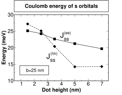
Another piece of information that decides the addition energies [Eq. (2)] is the Coulomb integral between the particles [Eq. (12)]. We list the pseudopotential-calculated Coulomb energies of orbitals for electrons in the first row of Table 2 and for holes in the first row of Table 3. For electrons, 22 - 25 meV, and for holes 20 - 27 meV for typical dots. These numbers can be directly compared with experimental value from electron/hole charging experiments, since [Eq. (12)]. The typical experimental values of for electrons is about Drexler et al. (1994); Warburton et al. (1998); Bock et al. (2002) 19 - 27 meV and for holes Warburton et al. (1998); Bock et al. (2003); Reuter et al. (2005) 20 - 25 meV. We plot in Fig.4 for electrons and holes vs. height for base = 25 nm dots. For flat dots, the electron-electron Coulomb energy is smaller than that of holes . However, is larger than for taller dots. The crossover is at about 2.5 nm for the = 25 nm dots. Note that in our calculation, the two nearly degenerate electron orbitals and , are spatially almost orthogonal to each other. However, in the simple 2D-EMA model,Warburton et al. (1998) the two degenerate orbitals and have same spatial function differing only by a phase factor. As a result, the exchange interaction between and is much smaller than that of and . Furthermore, the simple 2D-EMA model predicts , which is not true in the atomistic description, where is much smaller than and .
In a 2D-EMA model, there is only one free parameter in calculating the Coulomb integrals for each type of carriers: the effective length for electrons and for holes. This leads to simple geometric relationships as illustrated in Eq. (17). These relations are listed in the second column of Tables 2 and 3. However, as noted in Sec. II.3, a detailed analysis of atomistic wave functions He et al. (2004); Narvaez et al. (2005) show that they are not of pure conduction band character for electrons or HH, LH characters for holes; nor do they have pure , angular momentum characters as predicted by 2D-EMA model. Since inter-valley, inter-band coupling and the underlying atomistic symmetries are also ignored in the 2D-EMA model, we might expect that the simple relations between the Coulomb integrals of Eq. (17) must be somehow different in the atomistic approach relative to those predicted by the EMA, even for rather flat lens-shaped dots having parabolic-like energy level pattern, , as chosen here.
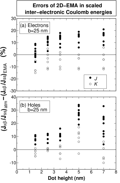
The ratios and derived from atomistic calculations are compared with the 2D-EMA model relationships in Table 2 for electrons and in Table 3 for holes for dots of different aspect ratios. To visualize the differences, we also plot the relative error for Coulomb energies and for exchange energies in Fig. 5 (a) for electrons and in Fig. 5(b) for holes, where “atm” means atomistic results and “EMA” means the 2D-EMA model results. For flat lens-shaped dots which have a parabolic-like level spectrum, we see qualitative agreement between the atomistic calculations and the 2D-EMA model. For such flat dots, the errors are generally within 20% of . For taller dots, the agreement is worse, as can be seen from Fig. 5. For even taller QDs (e.g., height/base 5/25 nm), the large biaxial strain will develop a “hole trap” at the InAs/GaAs interface, which lead to the hole localization on the interface of the dots.He et al. (2004); Narvaez et al. (2005) In these cases, where the hole (envelope) wave functions are totally different from those predicted by 2D-EMA model, the relationship between Coulomb and exchange energies are, accordingly, very different from those of 2D-EMA model.
At first sight, it would seem that if the values of in the 2D-EMA model are taken to be those calculated atomistically, the Coulomb integrals predicted by 2D-EMA model are only a few meV off from those calculated by atomistic theories. However, these small differences will change significantly the electronic phase-diagrams of carriers, as we will see below.
III.3 Ground state configurations: atomistic vs. 2D-EMA description
III.3.1 Generic phase diagrams for 2D-EMA model
To calculate the addition energies, we first need to know the spin and orbital configurations of the few-particle ground state, which minimizes the energy of the -particle system. For an illustration, we first use the “single configuration approximation”, i.e., retain only the Slater determinants that have the same orbital degree of freedom, and keep the exchange (spin-spin) coupling between these Slater determinants. The ground states are those configurations that have the lowest total energy. For electrons, the calculated ground state for =1 - 6 are shown in Fig. 1, which shows that the electron charging pattern follows Hund’s rule. The ground state spin and orbital configurations for holes are listed in Table 4 for = 1 - 6 holes. In contrast to electrons, the hole charging patterns show complicated behaviors that defy the Hund’s rule and the Aufbau’s principle for most of the cases of =5, 6 holes.He et al.
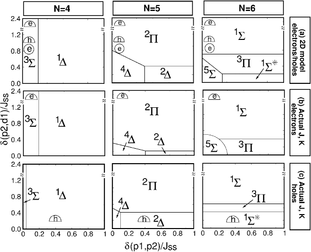
To understand the differences between the ground-state configurations of electrons and holes and the driving forces for these differences, we developed a general phase-diagram approach He et al. that classifies the many-particle configurations for electrons and holes in quantum dots in terms of simple electronic and geometric parameters. To do so, we calculate for each particle number , the configuration which minimizes the total-energy under the single-configuration approximation at different - splitting () and - energy spacing () using Coulomb integrals and in units of . This approach gives a phase diagram as a function of the parameters in units of , which yields for =4 two electronic phases:
| (18) |
Here, we have adopted a spectroscopic notation for a system with cylindrical symmetry. For , there are three possible phases:
| (19) |
For , we find four phases,
| (20) |
We first apply this approach to a 2D-EMA model. We relax the restrictions in 2D-EMA model of degenerate shells (=, ) and of equidistant shells () and allow and to vary. The resulting phase diagrams are shown in Fig. 6(a) for =4, 5 , 6.
III.3.2 Ground states for specific dots in the 2D-EMA model
To decide which of these phases is a ground state for a given dot, we need to know in Fig. 6(a) the actual value of and for this realistic dot. For electrons in self-assembled dots, the single-particle energy spacing is usually more than twice the Coulomb energy,Drexler et al. (1994); Warburton et al. (1998) i.e., . For holes, was determined from recent experimentsReuter et al. (2004, 2005) and is assumed in 2D-EMA model. This places in Fig. 6(a), for both electrons and holes, phases , , and as ground states for =4, 5, 6, respectively, where the lens represents a lens-shaped self-assembled QD, and label “e”, “h” inside the lens are symbols for electron and hole, respectively. As a comparison, we also show the electron ground-state phases for an electrostatic dot ( 50 nm) represented by a circle.
III.3.3 Generic phase diagrams for atomistic approach
We now use atomistic Coulomb and exchange energies and , listed in Table 2 and 3 to recalculate the phase diagram for electrons and holes in Figs. 6(b) and Figs. 6(c), respectively. We see that the phase boundaries change dramatically for both electrons and holes.He et al. For example, for =6 electrons, phase disappears [Fig.6(b)], while phase disappear for =5 holes.
| Height/Base (nm) | =1 | =2 | =3 | =4 | =5 | =6 |
|---|---|---|---|---|---|---|
| 2.5/20 | ||||||
| 3.5/20 | ||||||
| 2.5/25 | ||||||
| 3.5/25 | ||||||
| 2.5/27.5 | ||||||
| 3.5/27.5 |
III.3.4 Ground states for specific dots in the atomistic approach
We next use , and from Table 1 and 2 to decide the ground states for electrons in self-assemble InAs/GaAs QDs. For example, for a InAs/GaAs dot with 2.5 nm in height and 20 nm in base, we have 0.1 and 3. These parameters give the ground-state phase for 5 electrons, and the ground-state phase for 6 electrons. As we see, even though the phase boundaries calculated from atomistic theories are very different from those calculated from 2D-EMA model, the ground-state configurations are remain the same as those predicted by 2D-EMA model. This is because in the phase diagrams, the coordinates of the electrons in self-assembled dots are far away from other competing phases. For =4 electrons, the high spin state phase (Hund’s rule) and low spin state are relatively close in the phase diagram. The intrinsic -level splittings in the lens-shaped dots are about 1 - 4 meV (Table 1), which are smaller than the electron-electron exchange energies ( 5 mV), and therefore the ground state is the high-spin phase . However, if the dot shape is elongated, adding additional -level splittings, the ground state could be low-spin phase . Actually there are some experimental evidences showing that the ground state of 4 electrons could be a low spin state.Miller et al. (1997); Wibbelhoff et al. (2005)
In contrast to electrons, holes have , and large - splitting, small - splitting (Fig. 2), which place the holes in a different region in the phase diagrams than electrons, where there are more competing phases. For example, for the dot with base = 20 nm, and height =2.5 nm, we have 0.4 and 0.17. These relationships give, for this dot, the ground states , and for =4, 5, and 6 holes, respectively, showing a nontrivial hole charging pattern that breaks the Aufbau principle.He et al. We also list the ground state configurations for dots of different geometries in Table 4. As we see, in most of the cases, the ground states are still , and as shown in Fig. 6(c). However, there are some exceptions for very tall dots or very flat dots. For very flat dots (e.g., the / =2.5/27.5 nm dot), the - energy splitting (5.8 meV) is much smaller than the - energy splitting (9.4 meV), These parameters place the ground state of = 5 holes in phase and that of 6 holes in phase of Fig. 6(c). For very tall dots (e.g., the / = 3.5/20 nm dot), the interfacial hole localization changes the hole-hole Coulomb integrals dramatically, and thus change the phase boundaries in [Fig. 6(c)]. We find the ground states of the dot with / = 3.5/20 nm are and for 5 holes and 6 holes, respectively.
III.3.5 Effects of configuration interaction
If we use CI instead of single-configuration approximation, the ground states are superpositions of different configurations, but the leading CI configurations have a significant weight, being 79%, 71% and 64% for 4, 5, and 6 holes, respectively, in the / = 2.5/20 nm dot. Since the weights of leading configurations are significantly larger than other configurations, we are justified in using leading configurations to represent graphically the ground states. It is worth noting that for very large electrostatically confined dots, where single-particle energy spacing (down-left corner of the phase diagrams of Fig. 6), the ground state mixes large number of configurations, which have no significant leading configurations, and are therefore in strongly correlated states Yannouleas and Landman (2003) that are not discussed here.
| Height (nm) | 2.5 | 3.5 | 2.5 | 3.5 | 3.5 | 3.5 | 3.5 | 2.5 | 35 | |
|---|---|---|---|---|---|---|---|---|---|---|
| Base (nm) | 20 | 20 | 25 | 25 | 25 | 25 | 25 | 27.5 | 27.5 | |
| Ga comp. | 0 | 0 | 0 | 0 | 0.15 | 0.3 | 0.5 | 0 | 0 | Exptl. |
| 26.3 | 24.6 | 23.3 | 21.8 | 20.5 | 18.5 | 15.2 | 22.1 | 20.5 | 21.5 | |
| 89.5 | 84.4 | 71.8 | 67.6 | 61.2 | 53.2 | 40.3 | 65.2 | 60.8 | 57 | |
| 19.7 | 20.3 | 16.7 | 16.5 | 15.9 | 12.7 | 10.6 | 15.4 | 15.5 | 11.4 | |
| 21.5 | 19.5 | 20.1 | 18.5 | 16.6 | 16.5 | 12.9 | 19.6 | 17.5 | 21.0 | |
| 19.7 | 20.3 | 16.7 | 16.5 | 15.8 | 12.4 | 10.3 | 15.4 | 15.4 | 12.2 | |
| 24.1 | 19.0 | 21.9 | 17.5 | 18.3 | 18.4 | 17.8 | 21.0 | 16.7 | 23.9 | |
| 28.7 | 21.7 | 27.2 | 21.2 | 23.0 | 23.6 | 22.6 | 26.4 | 20.6 | 34.2 | |
| 18.1 | 16.9 | 16.4 | 15.2 | 15.4 | 15.4 | 15.0 | 15.6 | 14.5 | 17.1 | |
| 26.4 | 21.6 | 25.4 | 20.8 | 23.2 | 21.7 | 19.3 | 23.8 | 20.5 | 23.2 | |
| 17.1 | 16.1 | 15.3 | 14.4 | 14.5 | 16.0 | 15.7 | 15.5 | 13.7 | 15.0 |
III.4 Calculated charging and addition energies
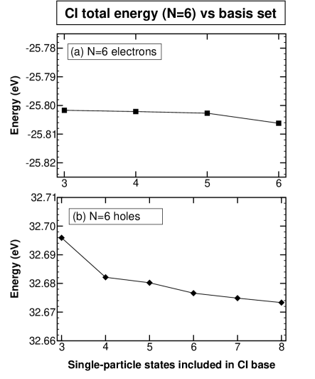
Once we determined the ground state configurations, we can calculate the total energies using Eq. (4). We calculate the ground state total energies for up to 6 electrons/holes for each dot. For electrons, in the CI approach we used 6 single-particle electron levels (, , , , , ) to construct all possible Slater determinants, while for holes, we used 8 single-particle hole levels. The total number of Slater determinants for 6 electrons is 924. For 6 holes, the total number of determinants is 8008. We plot in Fig. 7 the CI total energies for the ground state of 6 carriers vs. number of single-particle states included in the CI expansions. The total energies converge to about 1 meV if 6 single-particle states are used for electrons and 8 states are used for holes.
The charging energies and addition energies are calculated using Eq. (1) and Eq. (2). The addition energies calculated from CI calculations give results that are about 1 meV different from single-configuration results for electrons, and 1 - 3 meV different for holes. The addition energies are summarized in Table 5. Experimentally, the charging energies of electrons Drexler et al. (1994); Fricke et al. (1996); Miller et al. (1997) and holes Reuter et al. (2004, 2005) in self-assembled QDs are usually measured via capacitance spectroscopy, using gated structures.foo (c) The (In,Ga)As/GaAs dots used in the electron charging experiments were roughly estimated to be 7 nm in height and 20 nm in base in Refs. Fricke et al., 1996; Miller et al., 1997. The measured 23 meV in Ref. Fricke et al., 1996 and 21.5 meV in Ref. Miller et al., 1997, which, as shown in Sec. II, equals roughly , the electron-electron Coulomb interaction of orbitals. The charging energies between and levels, was estimated to be 57.0 meV in Ref. Miller et al., 1997. The average addition energies between -states are estimated to be 18 meV in Ref. Fricke et al., 1996, and 14 meV in Ref. Miller et al., 1997. Furthermore, in Ref. Miller et al., 1997, is almost twice as large as and , which might be related to the breakdown of Hund’s rule as a consequence of irregular shape of the dots. These results are listed in Table 5 and compared with our theoretical results. We see that the electron addition energies of an (In,Ga)As/GaAs dot, with / = 3.5/25 nm and Ga composition = 0.15, agree very well with the above experimental results, which show = 20.5 meV, = 61.2 meV, and the average addition energies between -states of about 16 meV.
The experimental hole addition energies are taken from Ref. Reuter et al., 2005, which gives =23.9 meV, comparable to that of . However, the addition energy between and orbitals, =34.2 meV, is significantly smaller than 57 meV. This result reflects that the - energy spacing of holes is much smaller than that of electrons. As seen from Table 5, our calculated addition energies of pure and flat (height=2.5 nm) InAs/GaAs dots agree very well with this experiment.
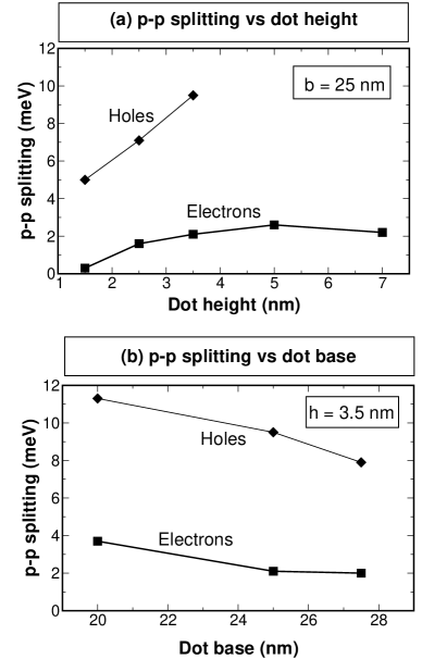
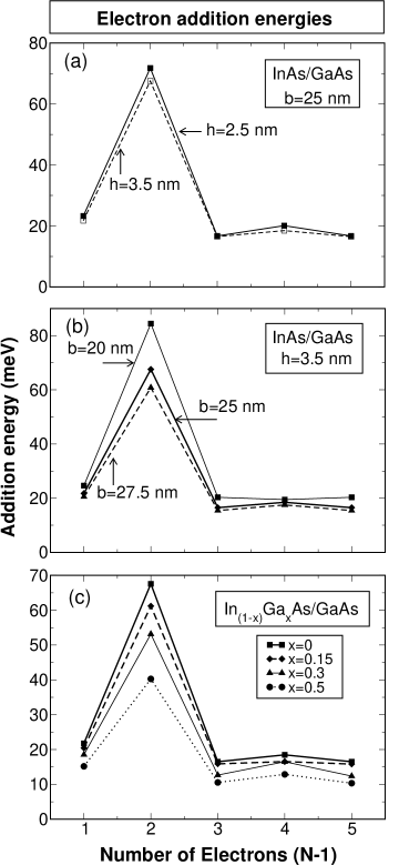
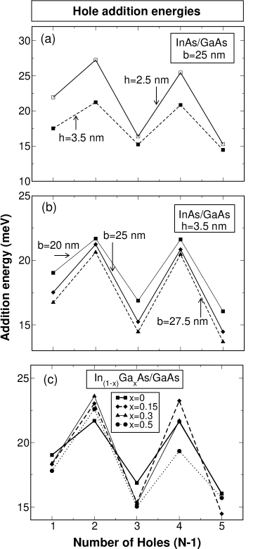
To study trends of addition energies for the electrons and the holes, we depict the electron addition energies for different dot heights [Fig. 8(a)], bases [Fig. 8(b)] and alloy compositions [Fig. 8(c)]. Similarly, the hole addition energies are plotted in Figs. 9 (a), 9(b), and 9(c) for dot heights, bases and alloy compositions. We see the following:
(i) Up to six carriers, the electron addition energies have a single peak at ()=2. The peak is due to the single-particle energy gap between the -shell and -shell. On the other hand, all hole addition energies have two peaks at ()=2 and ()=4 respectively, where the first peak come from the single-particle energy gap between the orbital and orbital and the second peak is associated with the energy difference between the and higher energy orbitals.
(ii) Electron addition energies decrease with increasing height and base of the dots, and the hole addition energies share the same trend. However, the electron addition energies are more sensitive to the base of the dots and relatively insensitive to the height. In contrast, the hole addition energies are very sensitive to the heights of the dot, and relatively insensitive to the base. This dependence suggests that the electron wave functions are more 2-dimensional like in the QDs, while hole wave functions are more extended in [001] direction.
(iii) Electron addition energies show a simple trend for alloyed In1-xGaxAs/GaAs QDs, which are consistently smaller for Ga rich dots. However, the hole addition energies of alloy dots show more complicated behaviors. The reasons of this complication are the following: (1) alloy dots have different trends in hole single-particle energy level spacings (see Table 1); (2) the ground state configurations might be different for different alloy compositions.
IV summary
We systematically studied the electron/hole addition energy spectra using single-particle pseudopotential plus many-particle CI methods. Considering the single-particle step, we find for electrons that there is a shell structure and that the - and - splittings are about 1 - 4 meV depending on the dot geometry. For holes, the single-particle step reveals large (5 - 11 meV) - splitting and absence of a well defined shell structure. Considering the - and - Coulomb integrals, we find that atomistically calculated ratios between various Coulomb integrals differ by about 20% from those in the 2D-EMA model calculation. These differences lead to many-particle phase diagrams that differ significantly from those predicted by the 2D-EMA model. In particular, the “unusual” hole single-particle spectrum and Coulomb integrals lead to many-particle ground states that defy the Hund’s rule and the Aufubau principle for holes. The predicted ground-state configurations and the addition energies calculated in this pseudopotential plus CI scheme compare well with experiments.
Acknowledgements.
We thank G. Bester and G. A. Narvaez for fruitful discussions. This work was funded by the U.S. Department of Energy, Office of Science, Basic Energy Science, Materials Sciences and Engineering, LAB-17 initiative, under Contract No. DE-AC36-99GO10337 to NREL.References
- Banin et al. (1999) U. Banin, Y. W. Cao, D. Katz, and O. Millo, Nature 400 (1999).
- Kastner (1993) M. Kastner, Physics Today 46, 24 (1993).
- Tarucha et al. (1996) S. Tarucha, D. G. Austing, T. Honda, R. J. van der Hage, and L. P. Kouwenhoven, Phys. Rev. Lett. 77, 3613 (1996).
- Drexler et al. (1994) H. Drexler, D. Leonard, W. Hansen, J. P. Kotthaus, and P. M. Petroff, Phys. Rev. Lett. 73, 2252 (1994).
- Fricke et al. (1996) M. Fricke, A. Lorke, J. Kotthaus, G. MedeirosRibeiro, and P. M. Petroff, Europhys. Lett. 36, 197 (1996).
- Miller et al. (1997) B. T. Miller, W. Hansen, S. Manus, R. J. Luyken, A. Lorke, J. P. Kotthaus, S. Huant, G. Medeiros-Ribeiro, and P. M. Petroff, Phys. Rev. B 56, 6764 (1997).
- Kouwenhoven et al. (1997) L. P. Kouwenhoven, T. H. Oosterkamp, M. Danoesastro, M. Eto, D. G. Austing, T. Honda, and S. Tarucha, Science 278, 1788 (1997).
- Bödefeld et al. (1999) M. C. Bödefeld, R. J. Warburton, K. Karrai, J. P. Kotthaus, G. Medeiros-Ribeiro, and P. M. Petroff, Appl. Phys. Lett. 74, 1839 (1999).
- Regelman et al. (2001) D. V. Regelman, E. Dekel, D. Gershoni, E. Ehrenfreund, A. J. Williamson, J. Shumway, A. Zunger, W. V. Schoenfeld, and P. M. Petroff, Phys. Rev. B 64, 165301 (2001).
- Warburton et al. (2000) R. J. Warburton, C. Schaflein, D. Haft, F. Bickel, A. Lorke, K. Karrai, J. M. Garcia, W. Schoenfeld, and P. M. Petroff, Nature 405, 926 (2000).
- Reuter et al. (2005) D. Reuter, P. Kailuweit, A. D. Wieck, U. Zeitler, O. Wibbelhoff, C. Meier, A. Lorke, and J. C. Maan, Phys. Rev. Lett. 94, 026808 (2005).
- Banin et al. (1998) U. Banin, C. J. Lee, A. A. Guzelian, A. V. Kadavanich, A. P. Alivisatos, W. Jaskolski, G. W. Bryant, A. L. Efros, , and M. Rosen, J. Chem. Phys. 109, 2306 (1998).
- Reuter et al. (2004) D. Reuter, P. Schafmeister, P. Kailuweit, and A. D. Wieck, Physica E 21, 445 (2004).
- Jacak et al. (1998) L. Jacak, P. Hawrylak, and A. Wójs, Quantum dots (Springer-Verlag, 1998).
- Wojs and Hawrylak (1996) A. Wojs and P. Hawrylak, Phys. Rev. B 53, 10841 (1996).
- Warburton et al. (1998) R. J. Warburton, B. T. Miller, C. S. Durr, C. Bodefeld, K. Karrai, J. P. Kotthaus, G. Medeiros-Ribeiro, P. M. Petroff, and S. Huant, Phys. Rev. B 58, 16221 (1998).
- Rontani et al. (1998) M. Rontani, F. Rossi, F. Manghi, and E. Molinari, Appl. Phys. Lett. 72, 957 (1998).
- (18) L. He, G. Bester, and A. Zunger, Phys. Rev. Lett. (in press).
- Williamson et al. (2000) A. J. Williamson, L.-W. Wang, and A. Zunger, Phys. Rev. B 62, 12963 (2000).
- Bester and Zunger (2003) G. Bester and A. Zunger, Phys. Rev. B 68, 073309 (2003).
- Bester and Zunger (2005) G. Bester and A. Zunger, Phys. Rev. B 71, 045318 (2005).
- Franceschetti and Zunger (2000) A. Franceschetti and A. Zunger, Europhys. Lett. 50, 243 (2000).
- Szabo and Ostlund (1996) A. Szabo and N. S. Ostlund, Modern Quantum Chemistry: Introduction to Advanced Electronic Structure Theory (Dover Pubns, 1996).
- Cohen and Bergstresser (1966) M. L. Cohen and T. K. Bergstresser, Phys. Rev. 141, 789 (1966).
- Wang and Zunger (1995) L. W. Wang and A. Zunger, Phys. Rev. B 51, 17398 (1995).
- Fu et al. (1997a) H. Fu, , and A. Zunger, Phys. Rev. B 55, 1642 (1997a).
- Fu et al. (1997b) H. Fu, , and A. Zunger, Phys. Rev. B 56, 1496 (1997b).
- Wang and Zunger (1999) L.-W. Wang and A. Zunger, Phys. Rev. B 59, 15806 (1999).
- Magri and Zunger (2002) R. Magri and A. Zunger, Phys. Rev. B 65, 165302 (2002).
- Zunger (2002) A. Zunger, Phys. Stat. Sol. (a) 190, 467 (2002).
- He et al. (2004) L. He, G. Bester, and A. Zunger, Phys. Rev. B 70, 235316 (2004).
- Dekel et al. (2000) E. Dekel, D. Gershoni, E. Ehrenfreund, J. M. Garcia, and P. M. Petroff, Phys. Rev. B 61, 11009 (2000).
- Bimberg et al. (1999) D. Bimberg, M. Grundmann, and N. N. Ledentsov, Quantum Dot Heterostructures (John Wiley & Sons, 1999).
- Fonseca et al. (1998) L. R. C. Fonseca, J. L. Jimenez, J. P. Leburton, and R. M. Martin, Phys. Rev. B 57, 4017 (1998).
- Bednarek et al. (2003) S. Bednarek, B. Szafran, K. Lis, and J. Adamowski, Phys. Rev. B 68, 155333 (2003).
- Shumway et al. (2001) J. Shumway, A. J. Williamson, A. Zunger, A. Passaseo, M. DeGiorgi, R. Cingolani, M. Catalano, and P. Crozier, Phys. Rev. B 64, 125302 (2001).
- Wang et al. (2000) L. W. Wang, A. J. Williamson, A. Zunger, H. Jiang, and J. Singh, Appl. Phys. Lett. 76, 339 (2000).
- Schmidt et al. (1996) K. H. Schmidt, G. Medeiros-Ribeiro, M. Oestreich, P. M. Petroff, and G. H. Dohler, Phys. Rev. B 54, 11346 (1996).
- Schmidt et al. (1998) K. H. Schmidt, G. Medeiros-Ribeiro, and P. M. Petroff, Phys. Rev. B 58, 3597 (1998).
- foo (a) For alloyed dots, the same dependence with height of the - spacing is find. See Ref. Narvaez et al., 2005.
- foo (b) The piezoelectric effect also contributes to the -state splitting of the electron states, as has been shown in Ref.Bester and Zunger, 2005. For the splitting of the hole states, the effect is more subtle. We find for a pure InAs lens shaped dot with 25 nm base and 3.5 nm height, using piezoelectric coefficients from bulk materials, that the hole - splitting without piezoelectric effect is 9.5 meV and with the piezoelectric effect is 9.7 meV, using piezoelectric coefficients from bulk materials. The change (0.2 meV) due to piezoelectric effects is rather small. We therefore ignored piezoelectric effects in our calculations.
- Sheng et al. (2005) W. Sheng, S. J. Cheng, and P. Hawrylak, Phys. Rev. B 71, 035316 (2005).
- Narvaez et al. (2005) G. A. Narvaez, G. Bester, and A. Zunger, J. Appl. Phys. 98, 043708 (2005).
- Bock et al. (2002) C. Bock, K. H. Schmidt, U. Kunze, V. V. Khorenko, S. Malzer, and G. H. Döhler, Physica E 13, 208 (2002).
- Bock et al. (2003) C. Bock, K. H. Schmidt, U. Kunz, S. Malzer, and G. H. Döhler, Appl. Phys. Lett. 82, 2071 (2003).
- Wibbelhoff et al. (2005) O. S. Wibbelhoff, A. Lorke, D. Reuter, and D. Wieck, Appl. Phys. Lett. 86, 092104 (2005).
- Yannouleas and Landman (2003) C. Yannouleas and U. Landman, Phys. Rev. B 68, 035326 (2003).
- foo (c) The electric fields applied to the dots are typically of the order of 50 kV/cm for electron charging devices (as gleaned from Ref. Drexler et al., 1994; Fricke et al., 1996; Miller et al., 1997) and 100 kV/cm for hole charging devices. Reuter et al. (2004, 2005) We performed additional calculations to estimate the effect of this field on the addition energies and obtained changes for addition energies to be about 1 meV at 100 kV/cm . We therefore ignored this correction in our calculations.