Spin relaxation of “upstream” electrons: beyond the drift diffusion model
Abstract
The classical drift diffusion (DD) model of spin transport treats spin relaxation via an empirical parameter known as the “spin diffusion length”. According to this model, the ensemble averaged spin of electrons drifting and diffusing in a solid decays exponentially with distance due to spin dephasing interactions. The characteristic length scale associated with this decay is the spin diffusion length. The DD model also predicts that this length is different for “upstream” electrons traveling in a decelerating electric field than for “downstream” electrons traveling in an accelerating field. However this picture ignores energy quantization in confined systems (e.g. quantum wires) and therefore fails to capture the non-trivial influence of subband structure on spin relaxation. Here we highlight this influence by simulating upstream spin transport in a multi-subband quantum wire, in the presence of D’yakonov-Perel’ spin relaxation, using a semi-classical model that accounts for the subband structure rigorously. We find that upstream spin transport has a complex dynamics that defies the simplistic definition of a “spin diffusion length”. In fact, spin does not decay exponentially or even monotonically with distance, and the drift diffusion picture fails to explain the qualitative behavior, let alone predict quantitative features accurately. Unrelated to spin transport, we also find that upstream electrons undergo a “population inversion” as a consequence of the energy dependence of the density of states in a quasi one-dimensional structure.
pacs:
72.25.Dc, 85.75.Hh, 73.21.Hb, 85.35.DsI Introduction
Spin transport in semiconductor structures is a subject of much interest from the perspective of both fundamental physics and device applications. A number of different formalisms have been used to study this problem, primary among which are a classical drift diffusion approach flatte1 ; flatte2 ; saikin1 , a kinetic theory approach wu , and a microscopic semiclassical approach bournel1 ; bournel2 ; bournel3 ; bournel4 ; saikin ; saikin1 ; pramanik_prb ; pramanik_apl . The central result of the drift diffusion approach is a differential equation that describes the spatial and temporal evolution of carriers with a certain spin polarization . Ref. saikin1 derived this equation for a number of special cases starting from the Wigner distribution function. In a coordinate system where the x-axis coincides with the direction of electric field driving transport, this equation is of the form:
| (1) |
where
| (5) |
is the diffusion coefficient, and and are dyadics (9-component tensors) that depend on , the mobility and the spin orbit interaction strength in the material.
Solutions of Equation (1), with appropriate boundary conditions, predict that the ensemble averaged spin = should decay exponentially with according to:
| (7) |
where
| (8) |
Here is the strength of the driving electric field and is a parameter related to the spin orbit interaction strength.
The quantity is the characteristic length over which decays to times its original value. Therefore, it is defined as the “spin diffusion length”. Equation (8) clearly shows that spin diffusion length depends on the sign of the electric field . It is smaller for upstream transport (when is positive) than for downstream transport (when is negative).
This difference assumes importance in the context of spin injection from a metallic ferromagnet into a semiconducting paramagnet. Ref. flatte1 pointed out that the spin injection efficiency across the interface between these materials depends on the difference between the quantities and where is the spin diffusion length in the semiconductor, is the conductivity of the semiconductor, is the conductivity of the metallic ferromagnet, and is the spin diffusion length in the metallic ferromagnet. Generally, . However, at sufficiently high retarding electric field, , so that . When this equality is established, the spin injection efficiency is maximized. Thus, ref. flatte1 claimed that it is possible to circumvent the infamous “conductivity mismatch” problem molenkamp , which inhibits efficient spin injection across a metal-semiconductor interface, by applying a high retarding electric field in the semiconductor close to the interface. A tunnel barrier between the ferromagnet and semiconductor rashba_tunnel or a Schottky barrier hanbicki1 ; hanbicki2 at the interface does essentially this and therefore improves spin injection.
The result of ref. flatte1 depends on the validity of the drift diffusion model and Equation (7) which predicts an exponential decay of spin polarization in space. Without the exponential decay, one cannot even define a “spin diffusion length” . The question then is whether one expects to see the exponential decay under all circumstances, particularly in quantum confined structures such as quantum wires. The answer to this question is in the negative. Equation (1), and similar equations derived within the drift diffusion model, do not account for energy quantization in quantum confined systems and neglect the influence of subband structure on spin depolarization. This is a serious shortcoming since in a semiconductor quantum wire, the spin orbit interaction strength is different in different subbands. It is this difference that results in D’yakonov-Perel’ (D-P) spin relaxation in quantum wires. Without this difference, the D-P relaxation will be completely absent in quantum wires and the corresponding spin diffusion length will be always infinite pramanik_transnano . The suband structure is therefore vital to spin relaxation.
II SEMICLASSICAL MODEL OF SPIN RELAXATION
In this paper, we have studied spin relaxation using a microscopic semiclassical model that is derived from the Liouville equation for the spin density matrix blum ; privman . Our model has been described in ref. pramanik_prb and wil not be repeated here. This model allows us to study D’yakonov-Perel’ spin relaxation taking into account the detailed subband structure in the system being studied.
In technologically important semiconductors, such as GaAs, spin relaxation is dominated by the D’yakonov-Perel’ (D-P) mechanism dp . This mechanism arises from the Dresselhaus dresselhaus and Rashba rashba spin orbit interactions that act as momentum dependent effective magnetic fields . An electron’s spin polarization vector precesses about according to the equation
| (9) |
where is the angular frequency of spin precession and is related to as , where is the electron’s effective mass. If the direction of B(k) changes randomly due to carrier scattering which changes k, then ensemble averaging over the spins of a large number of electrons will lead to a decay of the ensemble averaged spin in space and time. This is the physics of the D-P relaxation in bulk and quantum wells. In a quantum wire, the direction of k never changes (it is always along the axis of the wire) in spite of scattering. Nevertheless, there can be D-P relaxation in a multi-subband quantum wire, as we explain in the next paragraphs.
We will consider a quantum wire of rectangular cross-section with its axis along the [100] crystallographic orientation (which we label the x-axis), and a symmetry breaking electric field is applied along the y-axis to induce the Rashba interaction (refer Fig. 1). Then, the components of the vector due to the Dresselhaus and Rashba interactions are given by
| (10) |
where and are material constants, are the transverse subband indices, is the wavevector along the axis of the quantum wire, and are the transverse dimensions of the quantum wire along the z- and y-directions. Therefore,
| (11) | |||||
Thus, B (k) lies in the x-z plane and subtends an angle with the wire axis (x-axis) given by
| (12) |
Note from the above that in any given subband in a quantum wire, the direction of is fixed, irrespective of the magnitude of the wavevector , since is independent of . As a result, there is no D-P relaxation in any given subband, even in the presence of scattering.
However, is different in different subbands because the Dresselhaus interaction is different in different subbands. Consequently, as electrons transition between subbands because of inter-subband scattering, the angle , and therefore the direction of the effective magnetic field , changes. This causes D-P relaxation in a multi-subband quantum wire. Since spins precess about different axes in different subbands, ensemble averaging over electrons in all subbands results in a gradual decay of the net spin polarization. Thus, there is no D-P spin relaxation in a quantum wire if a single subband is occupied, but it is present if multiple subbands are occupied and inter-subband scattering occurs. This was shown rigorously in ref. pramanik_transnano .
The subband structure is therefore critical to D-P spin relaxation in a quantum wire. In fact, if a situation arises whereby all electrons transition to a single subband and remain there, further spin relaxation due to the D-P mechanism will cease thereafter. In this case, spin no longer decays, let alone decay exponentially with distance. Hence, spin depolarization (or spin relaxation) cannot be parameterized by a constant spin diffusion length.
The rest of this paper is organized as follows. In the next section, we describe our model system, followed by results and discussions in section IV. Finally, we conclude in section V.
III Model of upstream spin transport
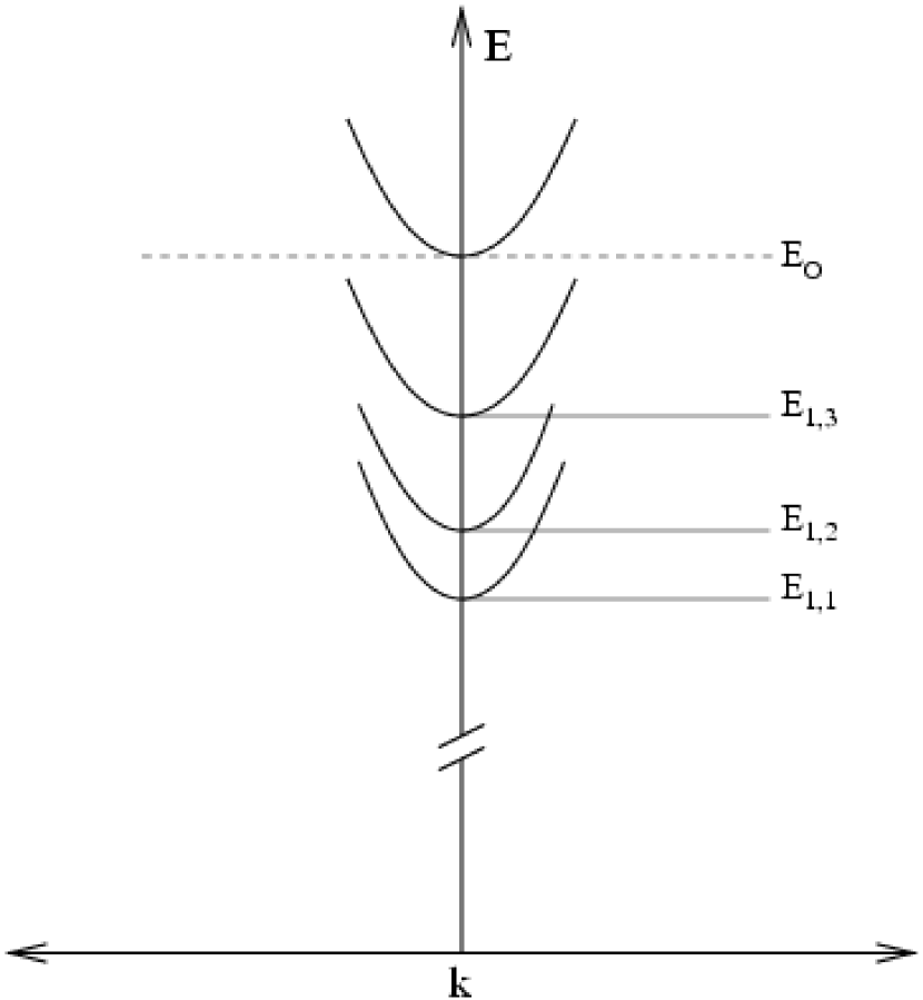
We consider a non centro-symmetric (e.g. GaAs) quantum wire with axis along [100] crystallographic direction. We choose a three dimensional Cartesian coordinate system with coinciding with the axis of the quantum wire (refer Fig. 1). The structure is of length with rectangular cross section: nm and nm. A metal gate is placed on the top (not shown in Fig. 1) to induce the symmetry breaking electric field , which causes the Rashba interaction. In a quantum wire defined by split Schottky gates on a two-dimensional electron gas, arises naturally because of the triangular potential confining carriers near the heterointerface. We assume kV/cm pramanik_prb . In addition, there is another electric field () which drives transport along the axis of the quantum wire. Consider the case when spin polarized monochromatic electrons are constantly injected into the channel at with injection velocities along . If these electrons occupy only the lowest subband at all times, then there will be no D’yakonov-Perel’ relaxation pramanik_transnano . Therefore, in order to study multisubband effect on spin dephasing of upstream electrons, we inject them with enough energy () that they initially occupy multiple subbands. We ignore any thermal broadening of injection energy saikin1 since for the range of temperature () considered, being Boltzmann constant. Let denote the energy at the bottom of th subband ( etc.). We place between the -th and -th subband bottoms as shown in Fig. 2. In other words, . We assume that the injected electrons, each with energy , are distributed uniformly over the lowest subbands. In other wordes, at time , electron population of the th subband is given by where is the total number of injected electrons and denotes their energies. At any subsequent time , these distributions spread out in space (), as well as in energy, due to interaction of the injected electrons with the electric field and numerous scattering events. Relative population of electrons among different subbands will change as well due to intersubband scattering events. Upstream electrons originally injected into, say, subband with velocity (), gradually slow down because of scattering and the decelerating electric field. They change their direction of motion (i.e. become downstream) beyond a distance measured from the injection point . Thus, no electrons will be found in the -th subband beyond . Note that the value of depends on three factors: the initial injection velocity into subband , the decelerating electric field and the scattering history. On the other hand, the ‘classical turning distance’ of monochromatic electrons injected into the -th subband with energy for a given electric field is given by
| (13) |
where is the energy at the bottom of the -th subband and is the injection velocity in the -th subband. Note that does not depend on scattering history and = in ballistic transport.
Clearly for a given (see Fig. 2). Thus, for a given channel electric field , min. Hence we concentrate on the region where, almost all injected electrons are upstream electrons. In the simulation, velocity of every electron is tracked and as soon as an electron alters direction and goes downstream (i.e. its velocity becomes positive) it is ignored by the simulator and another upstream electron is simultaneously injected from randomly in any of the lowest subbands with equal probability. This process is continued for a sufficiently long time till electron distributions over different subbands, , no longer change with time. Under this condition we say that steady state is achieved for the upstream electrons. This steady state electron distribution is extended from to and heavily skewed near the region . This steady state distribution of upstream electrons does not represent the local equilibrium electron distribution because of two reasons: (a) upstream electrons are constantly injected into the channel at ; this is the reason why the distribution is skewed near and (b) we exclude any downstream electron from the distribution. At local equilibrium, there will be of course both upstream and downstream electrons in the distribution.
The model above allows us to separate upstream electrons from downstream electrons and therefore permits us to study upstream electrons in isolation. Of course, in a real quantum wire, both upstream and downstream electrons will be present at any time, even in the presence of a strong electric field, since there will be always some non-vanishing contribution of back-scattered electrons to the upstream population.
The semiclassical model and the simulator used to simulate spin transport have been described in ref. pramanik_prb . Based on that model, at steady state, the magnitude of the ensemble averaged spin vector at any position inside the channel is given by
| (14) |
Here , , denotes the ensemble average of component of spin at position . Subscript implies that ensemble averaging is carried out over electrons only in the th subband. The above equation can be simplified to
| (15) |
where and is the angle between and . Note that in absence of any intersubband scattering event, for all (i.e. initial spin polarization of the injected electrons) pramanik_transnano . Simulation results that we present in the next section can be understood using Equation (15).
IV Results and Discussion
We examine how ensemble averaged spin polarization of upstream electrons varies in space for different values of driving electric field and injection energy () for a fixed lattice temperature . We vary in the range kV/cm for constant injection energy meV and = 30 K, where is measured from the bulk conduction band energy as shown in Fig. 2. The lowest subband bottom is 351 meV above the bulk conduction band edge. We also present results corresponding to meV with kV/cm and K. In all cases mentioned above, injection energies lie between subband 3 and subband 4. Injected electrons are equally distributed among the three lowest subbands initially. Obviously, this corresponds to a non-equilibrium situation. All injected electrons are 100% spin polarized transverse to the wire axis (i.e either or ).
Figures 3-6, 11, and 13 show how ensemble averaged spin components , , and of upstream electrons evolve over space. Figures 3-6 show the influence of the driving electric field on spin relaxation, Fig. 11 shows the influence of initial injection energy and Fig. 13 shows the influence of the intial spin polarization. It is evident that neither the driving electric field, nor the initial injection energy, nor the intial spin polarization has any significant effect on spin relaxation. Note that does not decay exponentially with distance, contrary to Equation (7). Spatial distribution of electrons over different subbands is shown in Fig. 7 - 10, and Fig. 12. The classical turning point of electrons in the third subband () has been indicated in each case. Fig. 7 - 10 show the influence of the driving electric field and Fig. 12 shows the influence of initial injection energy on the spatial evolution of subband population. As expected, decreases with increasing electric field in accordance with Equation (13). Note that at low electric field (Figs. 7 and 8) since all subbands are getting nearly depopulated of “upstream” electrons at = . Recall that only if transport is ballistic; therefore we can conclude that upstream transport is nearly ballistic in the range when 1 kV/cm. At high electric field, when 1.5 kV/cm, (Fig. 10) . This indicates that there are many upstream electrons even beyond the classical turning point. It can only happen if there is significant scattering that drives electrons against the electric field, making them go beyond the classical turning point. We can also deduce that most of these scattering events imparts momentum to the carriers to aid upstream motion rather than oppose it, since . This behavior is a consequence of the precise nature of the scattering events and would not have been accessible in drift-diffusion models that typically treat scattering via a relaxation time approximation.
IV.1 Population inversion of upstream electrons
Note that even though electrons are injected equally into all three subbands, most electrons end up in subband 3 – the highest subband occupied initially – soon after injection. Beyond a certain distance () subbands 1 and 2 become virtually depopulated. This feature is very counter-intuitive and represents a population inversion of upstream electrons! It can be understood as follows: scattering rate of an electron with energy is proportional to the density of the final state. In a quantum wire, density of states has dependence where is the energy at the bottom of the th subband. As the injected electrons move upstream they gradually cool down and their energies approach the energy at the bottom of subband 3 (). To visualize this, imagine the horizontal line in Fig. 2 sliding down with passage of time. As is approached, electrons will increasingly scatter into subband 3 since the density of final state in subband 3 is increasing rapidly. To scatter into a final state in subband 2 or 1 that has the same density of state as in subband 3 will require a much larger change in energy and hence a much more energetic phonon which is rare since the phonons obey Bose Einstein statistics. Therefore, subband 3 is the overwhelmingly preferred destination and this preference increases rapidly as electrons cool further. Consequently, beyond a certain distance, virtually all electrons are scattered to subband 3 leaving subbands 1 and 2 depleted. This feature is a peculiarity of quasi one-dimensional system and will not be observed in bulk or quantum wells. Exact values of and depend on injection energy and electric field. In the field range kV/cm and injection energy meV, . However, for higher values of electric field (e.g. 2kV/cm) or smaller values of injection energies, electrons reach classical turning point even before subbands 1 and 2 get depopulated.
Because of electron bunching in subband 3, spin dephasing in the region is governed by Equation (6) with . We observe a few subdued oscillations in in this region because of the “sine term” in Equation (15). However, in the region subbands 1 and 2 are almost depopulated. Therefore, there is no D-P relaxation in the interval since only a single subband is occupied pramanik_transnano . Consequently, the ensemble averaged spin assumes a constant value and does not change any more. Thus in this region, one can say that spin dephasing length becomes infinite. It should be noted that it is meaningless to study spin dephasing in the region because electrons do not even reach this region.
V Conclusion
In this paper, we have used a semiclassical model to study spin dephasing of upstream electrons in a quantum wire, taking into account the subband formation. We showed that the subband structure gives rise to rich features in the spin dephasing characteristics of upstream electrons that cannot be captured in models which fail to account for the precise physics of spin dephasing and the fact that it is different in different subbands. Because spin relaxation in a multi-subband quantum wire is non-exponential (even non-monotonic) in space, it does not make sense to invoke a “spin diffusion length”, let alone use such a heuristic parameter to model spin dephasing.
Finally, we have found a population inversion effect for upstream electrons. It is possible that downstream electrons also experience a similar population inversion. This scenario is currently being investigated.
Acknowledgement: The work at Virginia Commonwealth University is supported by the Air Force Office of Scientific Research under grant FA9550-04-1-0261.
References
- (1) Z. G. Yu and M. E. Flatté, Physical Review B, 66, 201202 (2002).
- (2) Z. G. Yu and M. E. Flatté, Physical Review B, 66, 235302 (2002).
- (3) S. Saikin, Journal of Physics: Condensed Matter, 16, 5071 (2004).
- (4) M. Q. Weng and M. W. Wu, Journal of Applied Physics, 93, 410 (2003).
- (5) A. Bournel, P. Dollfus, P. Bruno, and P. Hesto, The European Physical Journal Applied Physics, 4, 1 (1998).
- (6) A. Bournel, P. Dollfus, S. Galdin, F. -X. Musalem, and P. Hesto, Solid State Communications, 104, 85 (1997).
- (7) A. Bournel, P. Dollfus, P. Bruno, and P. Hesto, Materials Science Forum, 297-298, 205 (1999).
- (8) A. Bournel, V. Delmouly, P. Dollfus, G. Tremblay, and P. Hesto, Physica E, 10, 86 (2001).
- (9) S. Saikin, M. Shen, M. Cheng, and V. Privman, Journal of Applied Physics, 94, 1769 (2003).
- (10) S. Pramanik, S. Bandyopadhyay, and M. Cahay, Physical Review B, 68, 075313 (2003).
- (11) S. Pramanik, S. Bandyopadhyay, and M. Cahay, Applied Physics Letters, 84, 266 (2004).
- (12) M. I. D’yakonov and V. I. Perel’, Soviet Physics-Solid State, 13, 3023 (1972).
- (13) G. Schmidt, D. Ferrand, L. W. Molenkamp, A. T. Filip, and B. J. van Wees, Physical Review B, 62, R4790 (2000).
- (14) E. I. Rashba, Physical Review B, 62, R16267 (2000).
- (15) A. T. Hanbicki, B. T. Jonker, G. Itskos, G. Kioseoglou, and A. Petrou, Applied Physics Letters, 80, 1240 (2002).
- (16) A. T. Hanbicki, O. M. J. van’t Erve, R. Magno, G. Kioseoglou, C. H. Li, and B. T. Jonker, Applied Physics Letters, 82, 4092 (2003).
- (17) S. Pramanik, S. Bandyopadhyay, and M. Cahay, IEEE Transactions on Nanotechnology, 4, 2 (2005).
- (18) K. Blum, Density matrix theory and applications, 2nd edition, (Plenum Press, New York, 1996).
- (19) G. Dresselhaus, Physical Review, 100, 580 (1955).
- (20) Y. Bychkov and E. Rashba, Journal of Physics C: Solid State Physics, 17, 6039 (1984).
- (21) R. Elliott, Physical Review, 96, 266 (1954).
- (22) S. Saikin, D. Mozyrsky, and V. Privman, Nano Letters, 2, 651 (2002).
Figure captions :
Figure 1. A quantum wire structure of length with rectangular
cross section 30 nm 4 nm. A top gate (not shown) applies a symmetry breaking electric field
to induce the Rashba interaction. A battery (not shown) applies an electric
field (), along the channel. Monochromatic spin polarized electrons are
injected at with injection velocity . These electrons
travel along (upstream electrons) until their direction of
motion is reversed due to the electric field . We investigate spin
dephasing of these upstream electrons.
Figure 2. Subband energy dispersion in the quantum wire.
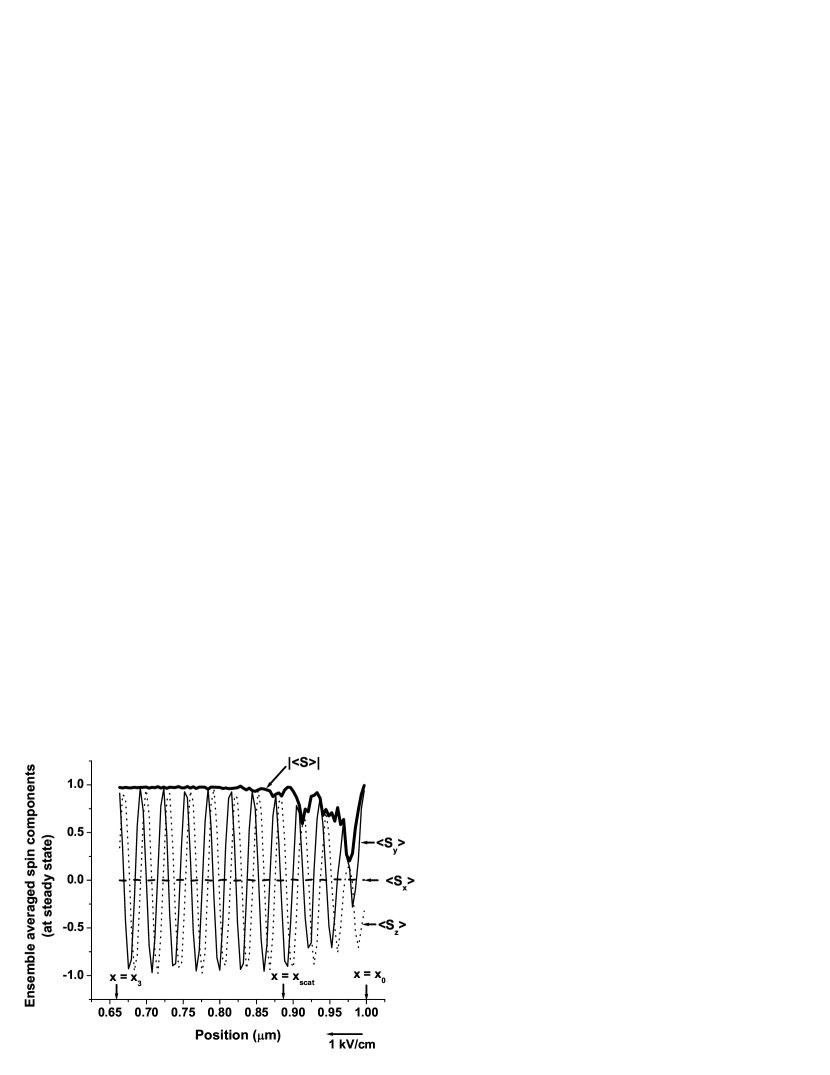
Figure 3. Spatial variation of ensemble averaged spin components for driving electric field = 0.5kV/cm at steady state.
Lattice temperature is K, injection energy meV. Electrons are injected with equal probability into the three lowest subbands. Classical turning point of subband electrons is denoted by and indicates the point along the channel axis where subbands and gets virtually depopulated. Injected electrons are polarized and is the point of injection.
Figure 4. Spatial variation of ensemble averaged spin components for driving electric field = 1kV/cm at steady state.
Other conditions are same as in Figure 3.
Figure 5. Spatial variation of ensemble averaged spin components for driving
electric field = 1.5kV/cm at steady state. Other conditions are same as in Figure 3.
Figure 6. Spatial variation of ensemble averaged spin components for driving
electric field = 2kV/cm at steady state. Other conditions are same as in Figure 3.
Figure 7. Spatial variation of electron population over different subbands at
steady state for driving electric field = 0.5 kV/cm.
Other conditions are same as before.
Figure 8. Spatial variation of electron population over different subbands
at steady state for driving electric field = 1 kV/cm.
Other conditions are same as before.
Figure 9. Spatial variation of electron population over different subbands
at steady state for driving electric field = 1.5 kV/cm.
Other conditions are same as before.
Figure 10. Spatial variation of electron population in different subbands
at steady state for driving electric field = 2 kV/cm.
Other conditions are same as before.
Figure 11. Spatial variation of ensemble averaged spin components for meV, kV/cm and lattice temperature K. Injected electrons
are polarized.
Figure 12. Spatial variation of electron population over different subbands at steady state for meV, kV/cm and lattice temperature K. Injected electrons are polarized.
Figure 13. Spatial variation of ensemble averaged spin components for meV, kV/cm and lattice temperature K. Injected electrons are polarized.