Local transport in a disorder-stabilized correlated insulating phase
Abstract
We report the experimental realization of a correlated insulating phase in 2D GaAs/AlGaAs heterostructures at low electron densities in a limited window of background disorder. This has been achieved at mesoscopic length scales, where the insulating phase is characterized by a universal hopping transport mechanism. Transport in this regime is determined only by the average electron separation, independent of the topology of background disorder. We have discussed this observation in terms of a pinned electron solid ground state, stabilized by mutual interplay of disorder and Coulomb interaction.
pacs:
73.21.-b, 73.20.QtIn the presence of Coulomb interaction, both magnetic field and disorder are predicted to stabilize many-body charge-ordered ground states. phases ; phase_B0 Strong perpendicular magnetic field quenches the vibrational motion of electrons, and has been extensively exploited to realize a charge-density wave (CDW) ground state in systems with weak background disorder. expt ; micro Despite the effort however, the nature of localization in such systems has been controversial, with both pinned Wigner solid (WS) formation and inhomogeneity-driven percolation transition being suggested. shashkin On the other hand, disorder stabilizes Coulomb correlation effects by introducing a pinning gap in the phonon density of states, which provides a long wavelength cutoff. phase_B0 This has led to the theoretical prediction of several forms of CDW ground states at zero or low . Systematic experimental investigations on such possibilities, however, have been rare, and form the subject of this work.
Increasing the magnitude of background potential fluctuations increases which stabilizes the CDW phases to higher temperatures. In modulation-doped GaAs/AlGaAs heterostructures, where disorder primarily arises from the charged dopant ions, efros depends strongly on the setback distance that separates the 2D electron system (2DES) and the dopants, where is the mean distance between the electrons in the 2DES. shklovskii1 ; chui However, disorder affects the ground state transport in two critical ways. First, presence of disintegrates the CDW phase into domains of finite size . At strong pinning, becomes microscopically small, leading to significant averaging in transport measurements with conventional macroscopic devices. Second, strong potential fluctuations can also result in a “freezing” of transport below a certain percolation threshold even when electron density () is relatively high, thereby making the regime of strong effective Coulomb interaction inaccessible.
Here, we show that these difficulties can be largely overcome by using modulation-doped heterostructures of mesoscopic dimensions. In such devices transport freezes at much lower in comparison to macroscopic devices at the same or disorder, thereby allowing transport at a large interaction parameter ( is the effective Bohr radius), even when is relatively small. Typical dimension of our devices in the current carrying direction was chosen to be m, which is also similar in order of magnitude to the suggested by recent microwave absorption studies for pinned WS ground states. micro The low- magnetotransport in these devices was found to display a striking universality in that the hopping distance in the localized regime was determined by , rather than the details of background disorder, indicating an unusual self-localization of electrons at sufficiently low .
| Wafer | Device | Doping | |||
|---|---|---|---|---|---|
| nm | cm-2 | mm | |||
| A2407 | A07a | 20 | 2.5 | ||
| A07b | 20 | 2.5 | |||
| A2678 | A78a | 40 | 2.5 | ||
| A78b | 40 | 2.5 | |||
| A2677 | A77 | 40 | 111The doping concentration of bulk doped devices is cm-3 over a range of 40nm. | Bulk | |
| A77L | 40 | 111The doping concentration of bulk doped devices is cm-3 over a range of 40nm. | Bulk | ||
| C2367 | C67 | 60 | 0.7 | ||
| T546 | T46 | 80 | 1.9 |
We have used Si modulation-doped GaAs/AlGaAs heterostructures where was varied from 20 nm to 80 nm. At a fixed , the effect of on the strength of potential fluctuations is reflected in the mobility , as can be observed from Fig. 1b. Both monolayer ()- and bulk-doped wafers were used. Relevant properties of the devices are given in Table I. Devices were cooled from room temperature to 4.2 K over 24 - 36 hours to allow maximal correlation in the dopant layer (redistribution of DX-centers). dopants This slow cooldown technique also lead to excellent reproducibility over repeated thermal cycles. Electrical measurements were carried out with standard low frequency (7.2 Hz) four-probe technique with excitation current of nA to minimize heating and other nonlinear effects. A direct measurement of within the microscopic region was carried out with an edge-state reflection-based technique. self1
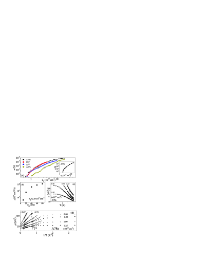
In Fig. 1a we compare the -scale of localization transition at and K in macroscopic and microscopic devices from the same wafer. In a standard mm Hall bar, as illustrated with wafer A2677, the linear conductivity (A77L: Inset of Fig. 1a) at times the compared to the mesoscopic sample (A77) from the same wafer. Further, in the large sample A77L shows excellent classical percolation-like scaling ( cm-2), where , implying a inhomogeneity-driven percolation transition at nonzero shashkin (solid line in inset of Fig. 1a). Similar scaling in the mesoscopic systems, however, was found to be difficult, with unphysically large estimates of (not shown), indicating a different mechanism of localization transition.
As is lowered below a sample-dependent characteristic scale (denoted by the crosses in Fig. 1a), onset of strong localization is identified by the resistivity () exceeding . At , the -dependence of at a fixed can be divided into three regimes, as illustrated with A78a: First, transport in the classical regime at is magnified in Fig. 1c, where is the Fermi temperature. In this regime , where (indicated by the solid line). As is decreased, the onset of the quantum regime () results in stronger increase in with decreasing . Note that the clear classical to quantum crossover implies a well-defined , and hence a uniform charge density distribution down to the lowest cm-2 (In A77L, inhomogeneity sets in at as large as cm-2). In the quantum regime and for , Fig. 1d shows that the behavior of is activated with , where is the activation energy. From the - and -dependence of the pre-exponential , we have shown earlier that the transport mechanism in this regime corresponds to nearest-neighbor hopping. self1 Below the characteristic scale K, variation of becomes weak, tending to a finite magnitude even in the strongly localized regime. This saturation in the insulating regime cannot be explained in terms of an elevated electron temperature due to insufficient thermal coupling to the lattice since depends only weakly on electron density up to (Fig. 1d), and the damping of Shubnikov-de Haas oscillations in the metallic regime shows the base electron temperature to be mK.
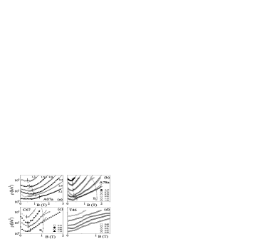
In order to explore the physical mechanism behind the weak -dependence of , we have carried out extensive magnetoresistivity (MR) measurements at the base . Figs. 2a to 2d show the -dependence of MR in the insulating regime of four devices with increasing from 20 nm to 80 nm. In general, we find a strong negative MR in A07, A78 and C67 at low , which can be attributed to interference of hopping paths. The negative MR is followed by an exponential rise in as is increased further. We have recently shown that the logarithm of such a positive MR at low varies in a quadratic manner with , i.e., , where and are -dependent factors. self1 Such a variation, denoted by the solid lines in Fig. 2, is found to be limited to , and extends over a -scale of , where was found to decrease rapidly as is increased. Note that in T46 (lowest disorder), neither a clear negative MR nor an exponential -dependence were observed. A physical significance of and of the qualitatively different MR behavior of T46 will be discussed later.
The observed behavior of can be naturally explained in the framework of tunnelling of electrons between two trap sites separated by a distance . In weak , such that the magnetic length , where is the localization length, the asymptotic form of the hydrogenic wave function changes from to . shklovskii This leads to a MR, , which implies
| (1) |
While depends on the tunnelling probability at , denotes the rate of change of this probability when is switched on. Importantly, both parameters provide information on the intersite distance , as well as independently. The parameter depends on the number of bonds at percolation threshold in the random resistor network (we shall subsequently assume ). Since conventional hopping sites are essentially impurity states, both and are expected to be strongly disorder dependent. Note that, since wave function overlap plays a critical role in transport, a direct source-to-drain tunnelling is ruled out in our case. savchenko
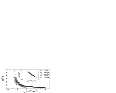
From the MR data we have evaluated and from the slope and intercept of the traces. Further details of the analysis can be found elsewhere. self1 In Fig. 3 we have shown as a function of for five different samples up to the corresponding . Strikingly, the absolute magnitudes of from different samples are strongly correlated, and can be described by an universal -dependent function over nearly two orders of magnitude. At stronger disorder (e.g., A07), localization occurs at a higher resulting in a lower , while at lower disorder (e.g. C67) localization occurs at lower yielding a larger magnitude of . This indicates that magnetotransport in such mesoscopic samples is not determined directly by disorder, but by in the localized regime. Qualitatively, the decreasing behavior of with increasing itself is inconsistent with the single-particle localization in an Anderson insulator. self1 ; fowler2
From the strong sample-to-sample correlation in the magnitude of , a disorder-associated origin of , is clearly unlikely. For example, taking will lead to distinct sets of for wafers with different . However, in the context of a pinned CDW ground state, another relevant length scale is . Indeed, in case of tunnelling events over a mean electron separation, i.e., , we find that Eq. 1 describes both absolute magnitude, as well as the -dependence of quantitatively. Using , Eq. 1 leads to , as indeed observed experimentally (solid line in the inset of Fig. 3). Allowing for sample-to-sample variation, we find T-2 from which, using Eq. 1, we get nm, which is close to in GaAs ( nm).
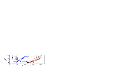
The analysis can be immediately checked for consistency from the -dependence of . From Fig. 4, we find that increases strongly with increasing when , as expected in the simple tunnelling framework (Eq. 1). In spite of the scatter, the overall slopes of the plots are similar in different samples (solid lines) with estimated to be nm, agreeing with that obtained from the analysis of . Note that the deviates from the exponential dependence, and tends to saturate as . While this is not completely understood at present, we note that the saturation in occurs within the range , irrespective of sample details. Similar universality in the hopping pre-exponential has been observed in the context of -dependence of in variable-range hopping, khondaker and has been suggested to indicate an electron-electron interaction mediated energy-transfer mechanism.
We now discuss the physical scenario which could lead to the electron separation-dependent hopping transport. We show that our observations can be explained in the theoretical framework of defect motion in a quantum solid that was originally developed by Andreev and Lifshitz in context of solid He3, AL and later adapted for a WS ground state. spivak ; pichard In our case, transport in both quantum and classical regime can be understood in terms of tunnelling of localized defects in an interaction-induced pinned electron solid phase as is reduced below the melting point . The defects, which act as quasiparticles at low , can arise from regular interstitials, vacancies, dislocation loops etc., as well as from zero-point vibration of individual lattice sites. AL The scale of zero-point fluctuation , is indeed strong in our case over the experimental range of , where is the interatomic interaction energy scale.
In the quantum regime, the transport at higher () is predicted to be thermally activated nearest-neighbor hopping of localized defects, while at lower () tunnelling of such defects leads to a -independent transport. AL While this clearly describes the weak -dependence of at low temperatures (Fig. 1d), the strongest support to this picture comes from the fact that the natural length scale of tunnelling is indeed the average electron separation . This immediately explains the unusual (or )-dependence of both and , as well as the apparent insensitivity of these parameters to local disorder. The negative MR at low caused by destruction of interference is then expected to persist up to a corresponding to (one flux quantum within an area of ), as indeed observed in our experiments (Fig. 2). The tunnelling of defect scenario also allows an estimate of the crossover scale , AL where is the bandwidth. For a pinned WS ground state, using the expression of in Ref.[8], experimentally measured , and , we find O[1 Kelvin] over the experimental range of in A78a, giving good order-of-magnitude agreement to the observed scale of . Finally, the behavior of in the classical regime ()(Fig. 1c) has also been recently observed, lilly and interpreted in terms of transport mediated by defect-type topological objects (Fermi-liquid droplets) in the WS phase. spivak
In presence of pinning, the MR-data suggests the asymptotic form of the wave function , where . However, the interplay of confinement arising from the magnetic potential and disorder pinning is expected to be critical in determining , with disorder pinning dominating at low . This is expected to result in the upper cutoff that decreases with decreasing disorder, as observed experimentally. The intricate interplay between disorder, electron-electron interaction and magnetic field is further illustrated by the absence of a clear dependence of the MR in T46 (largest ), which could be explained by a prohibitively small or the very instability of the solid phase at sufficiently low disorder. On the other hand, devices with nm showed inhomogeneity-driven Coulomb blockade oscillations in the localized regime, making the investigation of such a charge correlated state impossible. A quantitative understanding of the scale of , as well as the specific spatial structure of the ground state in the intermediate disorder regime, will require further investigations, which are presently in progress.
References
- (1) B. Tanatar and D. M. Ceperley, Phys. Rev. B 39, 5005 (1989); A. G. Eguiluz, A. A. Maradudin and R. J. Elliott, ibid. 27, 4933 (1983); A. A. Koulakov, M. M. Fogler and B. I. Shklovskii, Phys. Rev. Lett. 76, 499 (1996).
- (2) J. S. Thakur and D. Neilson, Phys. Rev. B 54, 7674 (1996); A. A. Slutskin, V. V. Slavin, and H. A. Kovtun, ibid. 61, 14184 (2000); G. Benenti, X. Waintal and J. -L. Pichard, Phys. Rev. Lett. 83, 1826 (1999); R. Jamei, S. Kivelson and B. Spivak, ibid. 94, 056805 (2005); S. T. Chui and B. Tanatar, ibid. 74, 458 (1995).
- (3) H. W. Jiang, R. L. Willet, H. L. Stormer, D. C. Tsui, L. N. Pfeiffer and K. W. West, Phys. Rev. Lett. 65, 633 (1990); V. Goldman, M. Santos, M. Shayegan and J. E. Cunningham, ibid. 65, 2189 (1990); H. Manoharan Y. W. Suen, M. B. Santos and M. Shayegan, ibid. 77, 1813 (1996); J. Yoon, C. C. Li, D. Shahar, D. C. Tsui and M. Shayegan, ibid. 82, 1744 (1999).
- (4) P. D. Ye, L. W. Engel, D. C. Tsui, R. M. Lewis, L. N. Pfeiffer and K. West, Phys. Rev. Lett. 89, 176802 (2002); Y. Chen, R. M. Lewis, L. W. Engel, D. C. Tsui, P. D. Ye, L. N. Pfeiffer and K. W. West, ibid. 91, 016801 (2003).
- (5) A. A. Shashkin, V. T. Dolgopolov, G. V. Kravchenko, M. Wendel, R. Schuster, J. P. Kotthaus, R. J. Haug, K. von Klitzing, K. Ploog, H. Nickel and W. Schlapp, Phys. Rev. Lett. 73, 3141 (1994); Y. Meir, ibid. 83, 3506 (1999); S. Das Sarma, M. P. Lilly, E. H. Hwang, L. N. Pfeiffer, K. W. West and J. L. Reno, ibid. 94, 136401 (2005).
- (6) A. L. Efros, Solid State Commun. 65, 1281 (1988); A. L. Efros, F. G. Pikus and V. G. Burnett, Phys. Rev. B 47, 2233 (1993).
- (7) I. M. Ruzin, S. Marianer and B. I. Shklovskii, Phys. Rev. B 46, 3999 (1992).
- (8) S. T. Chui, J. Phys.: Condens. Matter 5, L405 (1993).
- (9) E. Buks, M. Heiblum and H. Shtrikman, Phys. Rev. B 49, 14790 (1994); M. Stopa, ibid. 53, 9595 (1996).
- (10) A. Ghosh, M. Pepper, H. E. Beere and D. A. Ritchie, Phys. Rev. B 70, 233309 (2004).
- (11) B. I. Shklovskii, Fiz. Tekh. Poluprovodn. 17 2055 (1983) [Sov. Phys. Semicond. 17, 1311 (1983)]; B. I. Shklovskii and A. L. Efros, in Electronic Properties of Doped Semiconductors, Vol. 45 of Springer Series in Solid-State Sciences (Springer, Berlin, 1984).
- (12) A. K. Savchenko, V. V. Kuznetsov, A. Woolfe, D. R. Mace, M. Pepper, D. A. Ritchie and G. A. C. Jones, Phys. Rev. B 52, R17021 (1995).
- (13) G. Timp and A. B. Fowler, Phys. Rev. B 33, 4392 (1986).
- (14) S. I. Khondaker, I. S. Shlimak, J. T. Nicholls, M. Pepper and D. A. Ritchie , Phys. Rev. B 59, 4580 (1999); W. Mason, S. V. Kravchenko, G. E. Bowker and J. E. Furneaux, ibid. 52, 7857 (1995).
- (15) A. F. Andreev and I. M. Lifshitz, Zh. Eksp. Teor. Fiz. 56, 2057 (1969) [Sov. Phys. JETP 29, 1107 (1969)].
- (16) B. Spivak, Phys. Rev B 67, 125205 (2003).
- (17) G. Katomeris, F. Selva and J. -L. Pichard, Eur. Phys. J. B 31, 401 (2003), ibid. 33, 87 (2003).
- (18) H. Noh, M. P. Lilly, D. C. Tsui, J. A. Simmons, L. N. Pfeiffer and K. W. West, Phys. Rev. B 68, 241308(R) (2003).