Shot Noise Detection on a Carbon Nanotube Quantum Dot
Abstract
An on-chip detection scheme for high frequency signals is used to detect noise generated by a quantum dot formed in a single wall carbon nanotube. The noise detection is based on photon assisted tunneling in a superconductor-insulator-superconductor junction. Measurements of shot noise over a full Coulomb diamond are reported with excited states and inelastic cotunneling clearly resolved. Super-Poissonian noise is detected in the case of inelastic cotunneling.
pacs:
74.40.+k, 73.23.Hk, 73.21.La, 73.63.Fg, 73.63.KvThe study of shot noise, i.e. non-equilibrium current fluctuations due to the discreteness of charge carriers, is an important tool for studying correlations induced in mesoscopic transport by different types of interactions buttiker ; nazarov . Current is characterized by Poissonian shot noise when transport is determined by an uncorrelated stochastic process. Electron-electron interactions, such as Coulomb repulsion or resulting from the Pauli exclusion principle, can correlate electron motion and suppress shot noise. The noise power density is defined as the Fourier transform of the current-current correlator . This definition is valid both for positive and negative frequencies , corresponding to energy absorbtion or emission by the device gavish ; aguado ; schoelkopf . When ( is the voltage bias and the temperature), shot noise dominates over other types of noise and the power density has a white spectrum that can be expressed as . Here, is the average current and the Fano factor, , indicates the deviation from Poissonian shot noise for which . If the noise detector can not distinguish between emission and absorption processes, a symmetrized version is used. The Schottky formula refers to this symmetrized case.
For electron transport through a quantum dot (QD) shot noise can be either suppressed or enhanced with respect to the Poissonian value. First, for resonant tunneling, when a QD ground state is aligned between the Fermi levels in the leads, the Fano factor can vary between 1/2 and 1. The exact value is determined by the ratio of tunneling rates between the dot and the two leads theoryQD . For strongly asymmetric barriers transport is dominated by the most opaque one and shot noise is Poissonian. If the barriers are symmetric, the resonant charge state is occupied 50% of the time and a shot noise suppression is predicted. Second, when the QD is in Coulomb blockade, first-order sequential tunneling is energetically forbidden. Transport can still occur via cotunneling processes silvano , elastic or inelastic. These are second order processes, with a virtual intermediate state, allowing electron transfer between the leads. The elastic process leaves the QD in its ground state and transport is Poissonian. Inelastic cotunneling switches the system from a ground to an excited state and can lead to super-Poissonian noise with a Fano factor up to co-tunnoise . Experiments have shown shot noise suppression due to Coulomb blockade schoenenberger ; haug , but no experimental results exist on shot noise enhancement in the inelastic cotunneling regime. Here, we present the detection of noise, generated by a carbon nanotube quantum dot (CNT-QD). Excited states and inelastic cotunneling are clearly resolved in the noise measurements. For inelastic cotunneling we find super-Poissonian shot noise.
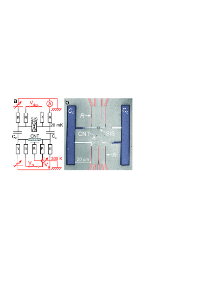
We use an on-chip noise detector consisting of a superconductor-insulator-superconductor (SIS) junction. Noise generated in the CNT-QD leads to photon assisted tunneling between the superconducting electrodes of the SIS detector (see Fig. 1(a),(b)). This causes a change in the detector current, that contains information about the spectral power of noise deblock . The frequency range of the SIS detector is determined by the superconducting gap (5-90 GHz for Al).
Sample fabrication necessitates five steps of e-beam lithography and material deposition for the different circuitry parts thesis . In intermediate steps CVD deposition NTgrowth and AFM imaging are used for growing and locating the nanotubes. A 20 nm Pt layer is deposited for contacts and the lower plate of the coupling capacitances (see Fig. 1(b)). For the insulating layer of the capacitances we use 40 nm of SiO. In a last step, angle evaporation with an intermediary oxidation step is employed to deposit the Al tunnel junctions for the SIS detector and the upper plate of the capacitances.
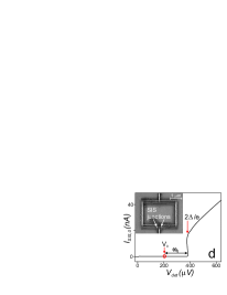
Current fluctuations in the CNT-QD, , induce, via the coupling capacitances, voltage fluctuations across the detector, . The detector current in absence of noise, , has a step-like shape (see Fig. 1(d)), which is modified by into . More specifically, the emission side of the spectrum induces a change in the superconducting gap region () thesis :
| (1) |
Note that only for . If we consider a detector voltage (see example in Fig. 1d) then only frequencies above contribute to the detector current. This means that each point on the detector curve represents noise detection over a bandwidth . However, contributions from different frequencies are normalized as , leading to smaller changes in the detector current for higher frequencies. Finally, is related to the CNT-QD current fluctuations by , with the transimpedance being determined by the coupling circuitry.
In the regime ( is the CNT bias voltage) shot noise dominates over other types of noise. Here, the power density is proportional to the average current, , and frequency independent (i.e. white spectrum). Eq.(1) can then be written as:
| (2) |
with a function that depends on transimpedance, detector characteristic in the absence of noise, and detector bias. Eq.(2) is valid in general, for any white noise source that is coupled to the SIS detector junction.
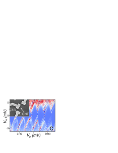
The single wall carbon nanotube (CNT) has a length of 1.6 m between the contacts and a side gate is used to change its electrical potential (see Inset of Fig. 1(c)). From the observation that we can induce both electron and hole transport at room temperature, we conclude that we have a small gap semiconductor CNT. After cooling to 20 mK, the conductance, , density plot, as a function of applied bias, , and gate voltage, , shows closing Coulomb diamonds, implying that one quantum dot is formed (see Fig. 1(c)). Excited states are clearly stronger for one direction (parallel to one side of the Coulomb diamonds) indicating asymmetric tunnel barriers to the leads. From the size of the larger Coulomb diamonds, we estimate the addition energy mV, with meV the orbital energy and meV the charging energy. The value for is consistent with the figure expected for a quantum dot formed by barriers at the contacts.
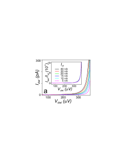

We fix the gate voltage at a Coulomb peak and current bias the nanotube. The detector signal, , presented as a function of the detector bias in Fig. 2, is increasing with the CNT current, . The fact that the normalized curves are all identical, over this range of (see inset of Fig. 2(a)), proves that we are indeed measuring white shot noise. This is also apparent from the inset of Fig. 2(b), showing that the integrated detector signal depends linearly on the nanotube current.
Since the power spectral density can be expressed as , the normalized curve can be written as . We determine the circuit calibration function by using a separate sample, in which well-known Poissonian noise is generated deblock . This calibration sample is fabricated simultaneously with the CNT sample, but with an SIS junction as a noise source. The obtained calibration curve is presented in Fig. 2(b). We also plot there the normalized curve , averaged for CNT currents between 5 nA and 40 nA. The two curves have similar amplitudes, meaning that, for a given value of the current through the source, the detector signal is the same for the two samples. This indicates a Fano factor close to the Poissonian value calibration1 for the high bias regime of the CNT. Based on these considerations, we use below the normalized curve, , in Fig. 2(b) as a calibration curve. We estimate that the deviation of the Fano factor from the value is less than 12% thesis . Our calibration allows for detection of changes in the Fano factor within this error bar.
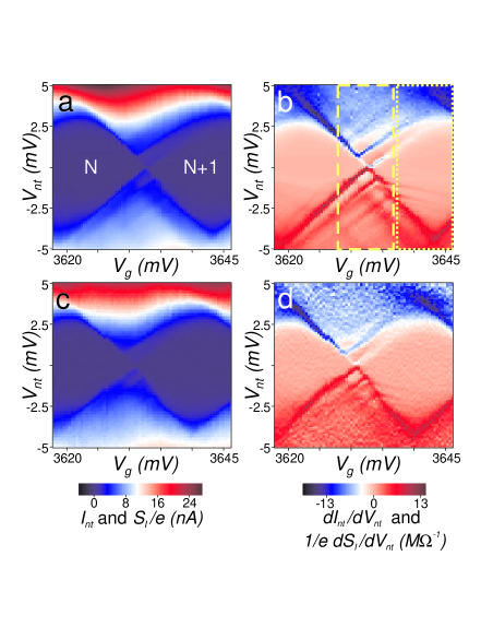
We now focus on the two adjacent Coulomb diamonds in Fig. 3(a), with its derivative plotted in Fig. 3(b). Subsequently, we use the SIS detector to measure shot noise. We fix the gate voltage, , and measure the detector current with finite () and zero () nanotube bias voltage, . Then the values for and are changed and the noise measurements repeated. In this way we obtain the detector signal over the entire range of the Coulomb diamond.
We sweep the detector bias only over a limited interval of the superconducting gap region, where the detector is most sensitive bias_sweep . We obtain the noise power over this interval from
| (3) |
The resulting density plots for noise (see Fig. 3(c) and (d)) are in good correspondence with the ones from the standard DC measurement (Fig. 3(a) and (b)). This is expected, as changes in also give changes in . There is a small shift in gate voltage values between the noise and the DC measurement (due to the long measurement time for noise detection). Excited states, as well as inelastic cotunneling signal inside the Coulomb diamond, are clearly resolved for both types of measurements.
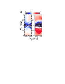
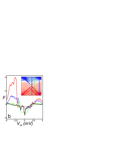
The density plot for the Fano factor can be obtained by dividing the plots in Fig. 3(c) and 3(a), after careful alignment to correct for small gate shifts. In this way we get the Fano factor values for specific regions outlined by the dashed and dotted lines in Fig. 3(b). These values, presented in Fig. 4(a), indicate a noise suppression () at the closing of the diamond (dashed part) and an enhancement of noise () in the regime of inelastic cotunneling (dotted part). Fano factor curves are also individually determined and plotted in Fig. 4(b).
We first consider the situation when the QD is outside Coulomb blockade (left part of Fig. 4(a) and black curve in Fig. 4(b)). For small biases, close to the diamond crossing, we find that noise is suppressed, . This indicates that transport is not dominated by a single barrier and resonance effects matter. At large biases (where also 5 nA) we detect Poissonian shot noise, in agreement with the calibration procedure. Thus, measurements in the sequential tunneling regime are consistent and prove that our detection scheme is reliable.
We now look at the region inside the Coulomb diamond, where transport occurs via cotunneling (see right part of Fig. 4(a)). First, for elastic cotunneling, no noise is measured ( in the dark-blue region). This is a second order process, in which an electron is transferred between the leads, via an intermediate virtual state. The electron has a very short dwell time and leaves the dot in its ground state. Subsequent elastic cotunneling events are completely uncorrelated and Poissonian shot noise is predicted, i.e. . However, our signal is obtained after subtracting the detector in the absence of device bias: . We only measure the excess noise (the noise induced by the CNT bias). In the regime of elastic cotunneling is too small ( pA) to give a measurable contribution to the excess noise, and our substraction procedure yields .
Finally we consider the inelastic cotunneling regime. The green curve in Fig. 4(b), taken at a gate value where inelastic cotunneling sets in, shows a small region in with super-Poissonian noise. The blue curve indicates an increase of the region with . Measurements of super-Poissonian noise, due to inelastic cotunneling, were also performed for other Coulomb diamonds (see red curve in Fig. 4(b)), showing a very pronounced Fano factor enhancement. Super-Poissonian noise can occur when two channels, with different transparencies, are available for transport co-tunnoise ; safonov . If only one can be open at a time, electrons are transferred in bunches whenever transport takes place through the more transparent channel. Such conditions are met by a quantum dot in the inelastic cotunneling regime. In the ground state, current is blocked due to Coulomb interaction. Still, if the bias is larger than splitting between the ground and the first excited state, a second order, inelastic tunneling processes can take place and an electron is transferred from one lead to the other. The inelastic cotunneling leaves the dot in the excited state. The electron can subsequently either tunnel out or relax to the ground state and block again the current. Thus, depending on the tunneling rate through the excited state and the relaxation rate, we can distinguish two regimes. If the electron relaxes to the ground state, we are in the weak cotunneling regime. For noise, this is equivalent to elastic cotunneling (the electron always relaxes and tunnels out from the ground state) and leads to Poissonian noise . If relaxation is slow and transport takes place through the excited state (strong cotunneling regime), electrons are transferred in bunches and the noise becomes super-Poissonian. For inelastic cotunneling we measure , showing that we are in the strong cotunneling regime. Still relaxation processes play an important role and lead to a Fano factor smaller than the maximum predicted value.
Noise measurement over the entire Coulomb diamond region of a QD is reported for the first time. Features present in the standard current measurements, including excited states and inelastic cotunneling, are clearly resolved in noise measurements. This confirms the high sensitivity and versatility of our detection scheme. Super-Poissonian noise (), corresponding to inelastic cotunneling, is detected, also for the first time.
We are grateful to P. Jarillo-Herrero for assistance in the CNT fabrication. We acknowledge the technical support from R. Schouten and B. van der Enden. Financial support was provided by the Dutch Organisation for Fundamental Research (FOM).
References
- (1) Y. M. Blanter and M. Büttiker, Phys. Rep. 336, 1 (2000).
- (2) Quantum Noise in Mesoscopic Physics edited by Y. V. Nazarov (Kluwer, Dordrecht, 2003).
- (3) U. Gavish, Y. Levinson, and Y. Imry, Phys. Rev. B 62, R10637 (2000).
- (4) R. Aguado and L. P. Kouwenhoven, Phys. Rev. Lett. 84, 1986 (2000).
- (5) R. J. Schoelkopf et al. in nazarov .
- (6) J. H. Davies, P. Hyldgaard, S. Hershfield, and J. W. Wilkins, Phys. Rev. B 46, 9620 (1992).
- (7) S. De Franceschi et al., Phys. Rev. Lett. 86, 878 (2001).
- (8) E. V. Sukhorukov, G. Burkard, and D. Loss , Phys. Rev. B 63, 125315 (2001); A. Thielmann, M. H. Hettler, J. König, and G. Schön, Phys. Rev. B 71, 045341 (2005); ibid., Phys. Rev. Lett. 95, 146806 (2005); W. Belzig, Phys. Rev. B 71, 161301(R) (2005).
- (9) H. Birk, M. J. M. de Jong, and C. Schönenberger, Phys. Rev. Lett. 75, 1610 (1995).
- (10) A. Nauen et al., Phys. Rev. B 66, 161303(R) (2002); A. Nauen et al., Phys. Rev. B 70, 033305 (2004).
- (11) R. Deblock, E. Onac, L. Gurevich, and L. P. Kouwenhoven, Science 301, 203 (2003).
- (12) E. Onac, PhD thesis, TU Delft, September 2005.
- (13) J. Kong, et al., Nature 395, 878 (1998).
- (14) A higher curve for the CNT sample is in agreement with a larger CNT impedance k compared with k of the SIS junction used for calibration thesis .
- (15) The applied detector bias is between V and 400 V. Due to series resistances in the circuit, this results in a real detector bias between V and V. The corresponding cut-off frequencies GHz, respectively GHz, represent the lower limit for the detection bandwidth.
- (16) S. S. Safonov et al., Phys. Rev. Lett. 91, 136801 (2003).