Quasiparticle density of states in Bi2Sr2CaCu2O8+δ single crystals probed using tunneling spectroscopy at ultra-low temperatures in high magnetic fields.
Abstract
Break-junction tunneling spectroscopy at temperatures 30-50 mK in high magnetic field is used to directly probe the quasiparticle density of states within the energy gap in a single crystal Bi2212 high- superconductor. The measured tunneling conductances in the subgap region have a zero flat region with no evidence for a linear increase of the density of states with voltage. A number of tunnel break-junctions exhibited curves with a second energy gap structure at the average magnitude 2 mV. Our data cannot be explained by either a pure pairing or a pure pairing.
pacs:
74.72.Hs, 74.50.+rI Introduction
A careful investigation of the density of states (DOS) for quasiparticle excitations in high- copper oxide superconductors is essential for the understanding of the mechanism responsible for superconductivity. Tunneling spectroscopy has played an important role in verifying BCS theory in conventional superconductors. The conductance of a tunnel junction is directly proportional to the quasiparticle density of states. The fine structure found in the tunneling conductance at voltages above the energy gap is a direct proof that the electron-phonon interaction is the coupling mechanism for superconductivity in conventional superconductors. It is widely accepted that the high- superconductors (HTS) have symmetry of the order parameter. Among the HTS, Bi2Sr2CaCu2O8+d (Bi2212) has often been studied by the tunneling method. Although the tunneling characteristics obtained with Bi2212 single crystals show features related to the superconducting energy gap, the shape of the tunneling conductance vs is far from the ideal BCS density of states. The conductance curves reveal a strong broadening of the superconducting-gap structure, with a nonzero contribution at zero voltage and a linear increase in the subgap region (cusp-like feature) (see e.g. Ref.K.Kitazava, 1996; Hoogenboom et al., 2003). In addition, an unusual feature frequently observed in the tunneling data of Bi2212 is the “dip-hump” structure beyond the gap edge which is close to the resonant spin excitation energy.Zasadzinski et al. (2001)
In superconducting tunnel junctions, the difference between - and -wave symmetry leads to a significant change in the current-voltage () characteristics. For an intrinsic unshunted -wave superconductor-insulator-superconductor (SIS) junction, the zero-bias conductance should be exponentially small at low temperatures (especially in case of superconductors with high ). In contrast, if the order parameter has nodes and symmetry, the characteristics of the -wave SIS junction in the vicinity of the zero bias should have a finite slope and thus a nonzero conductance at zero voltage (see e.g. Ref. [K.Kitazava, 1996]). Experimental tunneling characteristics of -wave SIS junctions do not agree with the theoretical predictions. Won and Maki Won and Maki (1994) found that at low temperatures the subgap tunneling conductance should increase almost quadratically with . Whereas, Yamada and Suzuki Yamada and Suzuki (2002) have recently shown that for coherent tunneling, the tunneling conductance of a -wave SIS junction is distinctly different when compared to incoherent tunneling. The subgap region of the coherent SIS tunneling conductance is almost linear in . They find that the quasiparticle tunneling in a Bi2212 mesa is mostly coherent. In general, the symmetry and pairing mechanism of the superconducting state remains controversial. For this reason, it is important to measure the subgap tunneling DOS of SIS Bi2212 junctions at very low temperatures and at high magnetic fields. While the results of measurements of the superconducting energy gap in SIS junctions are insensitive to thermal broadening, measurement in the mK region are required to rule out thermal excitations as the origin of both the excess conductance at zero voltage and the broadening of the conductance peak.
Magnetic field is essential, firstly, in order to suppress the Josephson current, which makes the measurement of the subgap tunneling conductance difficult. Secondly, magnetic field is very useful to distinguish relevant information in tunneling data from anomalous features due to critical current effects in weak links of the junction and the Bi2212 single crystal. Finally, it is necessary to study the effect of the magnetic field on the subgap and gap structures in the tunneling spectra.
Over the last few years the local DOS in Bi2212 has often been studied spectroscopically using a scanning tunneling microscope (STM). During the process of the mechanical cleaning, the crystal breaks between the BiO planes of two adjacent half-unit cells.Lindberg et al. (1989) In the case of tunneling measurements performed on the BiO plane, the large separation between the tip and the pair of CuO2 planes (greater than 10 Å) precludes the possibility of tunneling directly into these planes. In this situation, the electronic states of planes other than CuO2 play a role in the tunneling process and must be taken into account.Misra et al. (2002) In contrast to STM, in a break-junction fabricated on Bi2212 single crystals by using a precision setup, the tunneling can occur along CuO2 planes because many plane edges are created. It should be pointed out that since Bi2212 single crystals can be easily cleaved, the possibility exists that the crystal shears along a plane rather than breaking cleanly, leading to the formation of a -axis junction, but we will argue later that the tunneling in our break junctions is most likely to be in the -plane. There are a number of articles that have shown that a mechanically controllable break junction is one of the better tunnel systems (see e.g. references Mandrus et al., 1993; van der Post et al., 1994; Zasadzinski et al., 2001). Breaking the crystal at cryogenic temperatures and in high vacuum (or in an inert cryogenic fluid) guarantees two atomically clean surfaces, thereby minimizing surface contamination. The distance between these surfaces can be mechanically controlled. Increasing the distance results in a smaller junction, which is eventually reduced to only a few atoms. It is possible to form a tunnel junction with a vacuum barrier between the two foremost atoms.van der Post et al. (1994) Although, in view of the technical complexity, this method has not been extensively applied, it has provided reliable results so far, especially in the case of Bi2212 single crystals. At the present time this is the only method which allows a tunneling investigations of Bi2212 single crystals at ultra-low temperatures. In this paper, we describe the first experimental study of the tunneling DOS in copper oxide HTS at temperatures 30-50 mK in high magnetic fields up to 26 T using high-quality break-junctions fabricated on Bi2212 single crystals. These investigations are an extension of our previous tunneling studies of the Bi-compound HTS.Vedeneev et al. (1994); Vedeneev et al. (2001a)
II Experiment
The Bi2212 single crystals were grown by a KCl-solution-melt free growth method.Gorina et al. (1993); Vedeneev et al. (2001a) It is known, that overdoping or underdoping of Bi2212 can be achieved by changes in the oxygen content or by cation substitutions.Villard et al. (1998); Ooi et al. (1998) The first method requires an annealing in oxygen or argon at very high temperatures. A careful characterization of the annealed samples reveals that changes in are always accompanied by a severe degradation of the sample quality. Kinoda et al. Kinoda et al. (2003) have showed also that the annealing in oxygen can substantially increase the gap inhomogeneity. For this reason we have used only high quality as grown single crystals in which, the substitution of trivalent Bi for divalent Sr during growth reduces the hole concentration in the CuO2 planes.Harris et al. (1997) As the Bi/Sr ratio increases, the number of holes doped into the system decreases, which therefore pushes the system towards the hole-underdoped regime. Very recently Eisaki et al. Eisaki et al. (2004) have shown that as the Bi/Sr ratio in Bi2+xSr2-xCaCu2O8+δ single crystals approached 1, increases from 82.4 K for to 91.4 K for , 92.6 K for , and eventually to 94.0 K. Bi2212 single crystals with the excess Bi have repeatedly been used in tunneling study of temperature and doping dependence of the superconducting gap and pseudogap (see e.g. Ref. Matsuda et al., 1999).
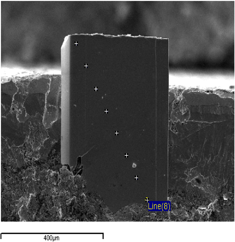
The quality of the crystals was verified by measurements of the dc resistance, ac susceptibility, X-ray diffraction and scanning electron microscopy. The single crystal showed X-ray rocking curves with a width of about demonstrating the high quality and high homogeneity of the samples. The values of the residual resistivity in our crystals were comparable with the lowest value previously reported for Bi2212. (see e.g. Ref. Watanabe et al., 1997). The composition of the crystals was studied using a Philips CM-30 electron microscopy with a Link analytical AN-95S energy dispersion X-ray spectrometer Gorina et al. (2005). The actual cationic compositions of each crystal investigated were measured at several different places on the crystal and the scatter in the data was less than 2%. In Fig. 1 we show a scanning electron micrograph of a crystal fragment where the composition measurement points are denoted by crosses. Previously, we have measured the Hall coefficient in several crystals and found the nearly linear relation between the excess Bi and the hole concentration . Our samples showed the well-known parabolic behavior for .
.
Since the deviation from conventional superconductivity should be most pronounced in the underdoped regime, for the present study, we have chosen three underdoped as grown single crystals Bi2.22Sr1.55Ca1.17Cu2.01O8+δ with = 84 K and transition width K. The same hole concentration for the investigated samples has been obtained from the Bi/Sr ratio as well as from the empirical relation which is satisfied for a number of the HTS.Tallon et al. (1995) We used the fact that the substitution of trivalent Bi for divalent Sr in the Bi-compounds reduces the hole concentration in the CuO2 planes.Harris et al. (1997)

.
In order to demonstrate that the investigated samples are underdoped, in Fig. 2 we show the temperature dependence of the in-plane resistivity for one of the investigating crystals (, ). For comparison, we show also for the overdoped () single crystal with the same K (midpoint) as well as the data for the slightly underdoped sample with K (). One can see that as in all Bi-compound HTS, the magnitude of increases with decreasing carrier concentration. A typical -linear behavior and a slightly upward curvature of are also seen in the slightly underdoped and the overdoped samples. Whereas for the underdoped sample (), deviates from high-temperature -linear behavior at a characteristic temperature (indicated by the arrow in Fig. 2), as would be expected. This temperature in Ref. [Watanabe et al., 2000] was identified as the pseudogap closing (opening) temperature . This is a further proof that we are measuring truly underdoped samples.
The dimensions of the investigated crystals were m. A four-probe contact configuration, with symmetrical positions of the low-resistance contacts () on both -surfaces of the sample was used. For the tunneling measurements, the sample was cooled to 30 mK at zero magnetic field. The tunnel junction was then fabricated in situ using a mechanical break junction technique. With the geometry of setup used, the break junctions forms so that tunneling occurs in the -plane. The characteristics and differential conductances as function of were measured using phase-sensitive detection techniques. We were able to fabricate a large number of tunnel break-junctions at different places along the initial break with resistances from 100 to 120 k (for bias voltages around mV) . Each junction was stable with reproducible characteristics at different magnetic fields. With our break-junction setup the magnetic field was oriented parallel to the CuO2 planes to an estimated accuracy of .Vedeneev et al. (1994)
In a previous investigation we have measured break junction tunneling together with the -plane and out-of-plane resistivities for the same Bi2212 crystal at different temperatures (4.2 - 250 K) for magnetic fields up to 20 T oriented parallel to the c-axis.Vedeneev et al. (1994) In a magnetic field reveals a significant increase in the width of the superconducting transition, while the value for the onset of superconductivity remained constant. The data for shows evidence for a strong suppression of the superconductivity along the -axis in a magnetic field of 20 T. The observed decrease of the value by a factor 2 indicates a significant reduction of the energy gap. In contrast, for all tunnel junctions investigated the energy gap is almost independent of magnetic field (-axis) T).Vedeneev et al. (1994) For this reason, we can formally state that the observed gap spectrum for our break junctions is related to the -plane superconducting energy gap and therefore to tunneling in the -plane. At the same time, we are unable to say anything about the tunneling direction in the -plane itself. For example, it was shown in Ref. [Wei et al., 1998] that the shape of spectra measured using point contact tunneling spectroscopy of YBa2Cu3O7 within the -plane in the [100] and [110] directions were quite different although the extracted magnitudes of the energy gap were in close agreement. The exact knowledge of the tunneling direction is essential for point contact tunneling spectroscopy where the main contribution to the quasiparticle current is given by Andreev reflection, which strongly depends on the wave vector. However, this is not the case for tunnel junctions. Hoogenboom et al. Hoogenboom et al. (2003) have shown on the basis of a detailed analysis of a large number of tunneling and ARPES spectra that the tunneling spectroscopy probes states along the entire Fermi surface.
III Break junction tunneling spectroscopy
.
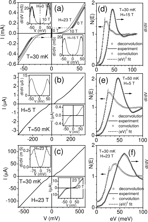
Fig.3(a-c) shows representative curves together with the tunneling conductances data for a 100 -, 115 k-, and a 6 k tunnel junction, respectively, at mK, for different magnetic fields (sample ). All the characteristics exhibit characteristic features typical for superconducting tunnel junctions, with a flat region around zero bias, consistent with the expected zero tunneling conductance (the insets in Fig.3 (a-c)), and a well-defined sharp increase in the tunnel current near mV connected with the superconducting gap. At large bias voltages up to V, the characteristics are linear with small deviation (increasing conductance) as expected for junctions with a good tunnel barrier without current leakage.Wolf (1985) The characteristics for the low-resistance tunnel junction in the subgap region (Fig.3(a)) are also typical for low-resistance Josephson junctions (the arrows indicate the direction of the bias current sweep during the measurements). The curves of this type were hysteretic (versus bias sweep direction) and have the slope of this switching. This is evident even from (Fig.3(a)). In accordance with the direction of the bias current sweep, the Josephson current in zero magnetic field equals -76 and +120 A. In our Bi2212 break-junctions we have observed the expected Fraunhofer-like dependence of the Josephson critical current as a function of magnetic field. The large period of Fraunhofer pattern points to the excessively small size of the tunnel junctions. After the suppression of the Josephson current in a magnetic field, the tunneling conductances of these junctions have a well-defined large zero flat region around zero bias voltage (the lower inset in Fig.3(a)). The high resistance junctions do not show a zero-bias peak even at T.
It should be pointed out that Joule heating effects could be important at the ultra low temperatures, especially for low impedance junctions. Previously we have studied Joule heating effects in break-junctions fabricated on Bi2212 Vedeneev et al. (1994) and Bi2Sr2CuO6+δ (Bi2201) Vedeneev et al. (2001b) single crystals. It was found that the shape of the tunneling conductance and the value of the zero-bias are very sensitive to a heating of the crystal region near the tunnel barrier. The characteristics in our data (Fig.3(a-c)) show no evidence whatsoever of heating. The linearity of the current-voltage characteristics at high bias voltages (up to 0.6 V) indicates that the heating caused by the current injection in our measurements is negligible. The shape of the tunneling conductance is unchanged despite a variation in the junction resistance of three orders of magnitude.
The measured tunneling conductances in the subgap region at mV can be fitted quite well to curves which are quadratic in . The tunneling conductances in case of the high-resistance tunnel junctions in Fig.3(b,c) in the subgap region do not show a large zero flat region. We have similar characteristics to those shown in Fig.3(a-c) for several tens of tunnel break-junctions formed on each of the three single crystals. We have never observed, either a linear increase of the tunneling conductances with voltage in the subgap region, or a nonzero zero-bias conductance for temperatures mK. The conductance spectra with a flat bottom seems at first sight to be consistent with -wave rather than -wave superconductivity. It should be pointed that the nonlinear subgap tunneling conductance in the vicinity of the zero bias has been observed previously in Bi2212 Mandrus et al. (1993); Vedeneev et al. (1994) and Hg-based cuprates Chen et al. (1994); Jeong et al. (1994) at 4.2 K, but the magnitudes of the background conductances at zero voltage were sizable, suggesting a significant density of states of quasiparticles at zero energy.
Our results are nevertheless puzzling since the tunneling conductances in the subgap region in -wave SIS junctions at mK-temperatures should have the zero flat region practically up to the gap voltages , and exhibit a very sharp conductance peak structure at . This is clearly not in agreement with our results. Despite the fact that the measurements were carried out at very low temperatures, the gap structure is strongly smeared with a broad conductance peak, and the shape of the tunneling spectra are not consistent with the expected tunneling conductance for -wave superconductors at temperatures near 0 K. On the other hand, the quadratic in behavior of the subgap tunneling conductances observed in this work is in agreement with the conductance of the SIS junction calculated by Won and Maki Won and Maki (1994) with -wave order parameter, although the shape of our experimental curves at voltages above the conductance peaks differs strongly from the theoretical curves.
IV Quasiparticle density of states
In order to extract the quasiparticle DOS, , from the tunneling conductances in Fig.3(a-c), we deconvoluted the expression for the normalized tunneling conductance Wolf (1985)
| (1) |
This expression suggests that a tunneling matrix element which weights a particular momentum direction is a constant and the tunneling spectrum directly relates to the DOS in the CuO2 plane. Although in some articles the tunneling spectrum was considered to be suggestive of an anisotropic matrix element, in Ref. [Hoogenboom et al., 2003] it was shown on the basis of a detailed analysis of the tunneling and ARPES spectra that the tunneling matrix element does not have a strong dependence on the wave vector. Tunneling spectroscopy therefore equally probes states over the entire Fermi surface.Hoogenboom et al. (2003)
An iterative procedure for the deconvolution together with the method used to obtain the normalized tunneling conductance is described in Ref. [Vedeneev et al., 1994]. In Fig. 3(d-f) the data points (squares) represent the result of this deconvolution for three different tunneling junctions from Fig.3(a-c), respectively. The solid lines show the experimental conductance curves compared with the calculated curves (circles) using the obtained from the deconvolution of Eq.(1). The good agreement with the data in Fig. 3(d-f) confirms the validity of the iterative procedure used to obtain . The shape of the showed in Figs.3(d-f) is fully compatible with a smeared BCS DOS for Bi2212.Vedeneev et al. (1994) The obtained over the entire subgap region can be fitted quite well to curves which are quadratic in (dashed lines). A quadratic rather than linear increase of in the subgap region seems to be strong evidence against -wave symmetry.
Note that a quadratic or nonlinear in subgap tunneling conductance in Bi2212 has been observed previously in STM experiments, for example in Ref. [Miyakawa et al., 1999; Misra et al., 2002; Renner et al., 1998]. Franz and Millis Franz and Millis (1998) have shown that a reasonable fit to the data in Ref. [Renner et al., 1998] assuming a DOS with a -wave order parameter could be made provided the tunneling matrix element is anisotropic. Assuming an isotropic (constant) matrix element leads to sharper V-shaped gap structure, inconsistent with the experimental data.Renner et al. (1998) As previously noted, the tunneling matrix element is most likely independent of the wave vector,Hoogenboom et al. (2003) which implies that the STM spectra give the quasiparticle DOS directly, and are therefore inconsistent with a pure -wave order parameter, in agreement with our results. For this reason, we are forced to conclude that it is not possible to explain our data in terms of either pure pairing or pure pairing. Our results lead to the conclusion that Bi2212, in all likelihood, has a mixed pair state, as has been repeatedly suggested in the literature (see e.g. Ref.Li1 et al., 1999; Latyshev et al., 2004).
V Sub-gap structure

In addition, a large number of the tunnel break-junctions exhibited curves with gap-like features within the gap at voltages mV. With increasing magnetic field this structure broadens, diminishes in amplitude and shifts to lower voltages. In Fig.4, we show the subgap regions of the differential conductances as a function of the bias voltage in different magnetic fields at mK. (a,b) - two tunnel break-junctions with resistance of nearly 1 k fabricated with the same single crystal (the low-voltage gap-like structure is indicated by arrows). The inset in (a) shows the full gap spectra at 0 and 26 T in order to compare the amplitude of the sub-gap features with the gap peak. Fig.4(c,d) shows the sub-gap regions of the spectra on an enlarged scale for two single crystals and (with resistances of around 300 ). For clarity, the curves in Fig.4(b-d) have been shifted vertically with respect to the lower curves.
It might be thought that the observed sub-gap structure are low-energy features related to the zero-bias peak which is caused by -wave Andreev bound states Fogelstrom et al. (1997); Covington et al. (1997) or the Josephson effect. However, in case of the higher-resistance break-junction (Fig.4(a)) the zero-bias peak is lacking at T. Nevertheless, both the sub-gap structure and its field dependence are seen. In Fig.4(b-d), the sub-gap gap-like structure is also clearly visible despite the fact that the zero-bias peak is suppressed completely by the magnetic field. This data show that the zero-bias peak and the sub-gap gap-like structure in our case have distinctly different origins.
Taking into account the magnetic field dependence of the gap-like structure observed here, we identify this feature with a small energy gap, the average magnitude of which is 2 mV. Electronic structure calculations for Bi2212 have long predicted the presence of BiO-derived bands and a splitting of CuO2 bands at the Fermi energy. If we assume that the break-junction tunneling averages the DOS equally around the Fermi surface,Hoogenboom et al. (2003) then the observed tunneling conductance must involve two separate order parameters derived from different bands. While the sub-gap structure might be connected with a proximity induced energy gap in the BiO layers,Yurgens et al. (1996) the possible existence of a second small gap (2 meV) in Bi2212 has been previously suggested by Shen et al. Shen et al. (1993), Mahan Mahan (1993) and Mallet et al. Mallet et al. (1996) in order to explain the gap anisotropy observed in ARPES and vacuum tunneling spectroscopy of Bi2212. It should be pointed out that the weak sub-gap structure in Bi2212 has been occasionally seen in the vicinity of the zero bias in STM spectra at 4.2 K Liu et al. (1994); Renner et al. (1998) and break-junctions at 10 K.Miyakawa et al. (1999) It is also possible that the sub-gap structure detected by us at mK temperatures can manifest itself as a “linear” increase in the subgap region in the vicinity of the zero bias as often observed in the STM spectra of Bi2212 measured at K.
VI Superconducting energy gap
We now turn our attention to the magnitude of the superconducting energy gap in the studied crystals. For the SIS junctions studied here, the peak-to-peak separation of the two main maxima of the curves must correspond to 4. As can be seen in Fig.3(a-c), this value is different for the different break-junctions formed using the same single crystal () and equals 96, 93, and 124 mV. The applied magnetic field -plane should decrease only slightly the peak-to-peak separation in curves due to the very high parallel critical magnetic field in Bi2212. For sample , we find a surprisingly wide scatter of the size of the energy gap 2 ranging from 46 to 78 mV for the more than 50 different break-junctions investigated. Similarly, for two other single crystals ( and ), we obtained 2 mV and 2 mV, respectively.

Miyakawa et al. Miyakawa et al. (1998, 1999) have found a strong monotonic dependence the superconducting energy gap of the Bi2212 on the doping concentration. However, we can formally exclude macroscopic sample inhomogeneity, as the origin of the observed variation, since 2= 46-78 meV would imply Miyakawa et al. (1998) a spread of hole concentration . Using the empirical relation for vs , this would imply values of ranging from 80 to 95 K. In addition, the chemical composition of the crystal, measured at several different points, is found to be identical (Fig.1). The crystal is of a very high quality judging from the sharp superconducting transition width K (in the magnetization measurements), and the small rocking curve width . Following reference Kinoda et al., 2003, this strongly suggests that such a wide range of the gap values originates from the presence of different superconducting regions on the scale of a few coherence lengths. The effects of a nanoscale chemical inhomogeneity on of Bi2212 was recently studied in Ref. [Eisaki et al., 2004]. If the sample has a nanoscale disorder with multiple energy gaps, the convolution of several DOS gives a strongly smeared single conductance peak (Fig.3(a-c)), nevertheless, the DOS after the deconvolution of the conductance can show an additional maximum in the peak region (Fig.3(f)). In individual cases the break-junctions can show double peaks in the conductance at voltages nearly 2 (Fig.5), that is indicative of two nanoscale superconducting regions in the region of the junction.
VII Conclusion
In conclusion, we have studied the tunneling density of states using high-quality break-junctions fabricated on Bi2212 single crystals. Our experiments provide a crucial test for the presence of excitations within the superconducting energy gap. The measured tunneling conductances in the subgap region show a zero flat region. We have never observed either a linear increase of the tunneling conductances with voltage in a subgap region or a nonzero zero-bias conductance at the temperatures 30-50 mK. The deconvoluted DOS in the whole subgap region can be fitted quite well to curves which are quadratic in . A quadratic rather than linear increase of in the subgap region seems to be strong evidence against pure symmetry. The major part of the tunnel break-junctions exhibited curves with the second energy gap structure with an average magnitude 2 mV. We cannot explain our data with either pure pairing or pure pairing. The wide range of the superconducting gap values observed suggests that the results of investigations of the doping dependence of the superconducting gap in HTS by tunneling spectroscopy need to be treated with care.
Acknowledgements.
This work has been partially supported by NATO grant PST.CLG. 979896.References
- K.Kitazava (1996) K.Kitazava, Science 271, 313 (1996).
- Hoogenboom et al. (2003) B. Hoogenboom, C. Berthod, M. Peter, O. Fischer, , and A. Kordyuk, Phys. Rev. B 67, 224502 (2003), and references cited therein.
- Zasadzinski et al. (2001) J. Zasadzinski, L. Ozyuzer, N. Miyakawa, K. Gray, D. Hinks, , and C. Kendziora, Phys. Rev.Lett. 87, 067005 (2001).
- Won and Maki (1994) H. Won and K. Maki, Phys. Rev. B 49, 1397 (1994).
- Yamada and Suzuki (2002) Y. Yamada and M. Suzuki, Phys. Rev. B 66, 132507 (2002), and references cited therein.
- Lindberg et al. (1989) P. A. P. Lindberg, Z. X. Shen, B. O. Wells, D. S. Dessau, D. B. Mitzi, I. Lindau, W. E. Spicer, and A. Kapitulnik, Phys. Rev. B 39, 2890 (1989).
- Misra et al. (2002) S. Misra, S. Oh, D. J. Hornbaker, T. DiLuccio, J. N. Eckstein, and A. Yazdani, Phys. Rev. Lett. 89, 087002 (2002).
- Mandrus et al. (1993) D. Mandrus, J. Hartge, C. Kendziora, L. Mihaly, and L. Forro, Europhys. Lett. 22, 199 (1993).
- van der Post et al. (1994) N. van der Post, E. T. Peters, I. K. Yanson, and J. M. van Ruitenbeek, Phys. Rev. Lett. 73, 2611 (1994).
- Vedeneev et al. (1994) S. I. Vedeneev, A. G. M. Jansen, P. Samuely, V. Stepanov, A. Tsvetkov, and P. Wyder, Phys. Rev. B 49, 9823 (1994).
- Vedeneev et al. (2001a) S. Vedeneev, A. Jansen, and P. Wyder, Physica B 300, 38 (2001a), (review article).
- Gorina et al. (1993) J. Gorina, G. Kaljuzhnaia, V. Ktitorov, V.P.Martovitsky, V. Rodin, V. Stepanov, A. Tsvetkov, and S.I.Vedeneev, Solid State Commun. 85, 695 (1993).
- Villard et al. (1998) G. Villard, D. Pelloquin, and A. Maignan, Phys. Rev. B 58, 15231 (1998).
- Ooi et al. (1998) S. Ooi, T. Shibauchi, and T. Tamegai, Physica C 302, 339 (1998).
- Kinoda et al. (2003) G. Kinoda, T. Hasegawa, S. Nakao, T. Hanaguri, K. Kitazawa, K. Shimizu, J. Shimoyama, and K. Kishio, Phys. Rev. B 67, 224509 (2003).
- Harris et al. (1997) J. Harris, P. White, Z.-X. Shen, H. Ikeda, R. Yoshizaki, H. Eisaki, S. Uchida, W. Si, J. Xiong, Z.-X. Zhao, et al., Phys. Rev. Lett. 79, 143 (1997).
- Eisaki et al. (2004) H. Eisaki, N. Kaneko, D. L. Feng, A. Damascelli, P. K. Mang, K. M. Shen, Z.-X. Shen, and M. Greven, Phys. Rev. B 69, 064512 (2004).
- Matsuda et al. (1999) A. Matsuda, S. Sugita, and T. Watanabe, Phys. Rev. B 60, 1377 (1999).
- Watanabe et al. (1997) T. Watanabe, T. Fujii, and A. Matsuda, Phys. Rev. Lett. 79, 2113 (1997).
- Gorina et al. (2005) Y. Gorina, G. Kaljuzhnaia, N. Sentyurina, V. Stepanov, and S. Chernook, Kristallografiya 50, 150 (2005), [Crystallography Reports 50, 142 (2005)].
- Tallon et al. (1995) J. Tallon, J. Cooper, P. de Silva, G. Williams, and J. Loram, Phys. Rev. Lett. 75, 4114 (1995).
- Watanabe et al. (2000) T. Watanabe, T. Fujii, and A. Matsuda, Phys. Rev. Lett. 84, 5848 (2000).
- Wei et al. (1998) J. Wei, N.-C. Yeh, D. Garrigus, and M. Strasik, Phys. Rev. Lett. 81, 2542 (1998).
- Wolf (1985) E. Wolf, Principles of electron tunneling spectroscopy (Oxford University Press, New York, 1985).
- Vedeneev et al. (2001b) S. I. Vedeneev, P. Szabo, A. G. M. Jansen, and I. S. Vedeneev, Zh. Eksp. Teor. Fiz. 119, 1 (2001b), [Sov. Phys. JETP 92, 851 (2001)].
- Chen et al. (1994) J. Chen, J. Zasadzinski, K. Gray, J. Wagner, and D. Hinks, Phys. Rev. B 49, 3683 (1994).
- Jeong et al. (1994) G. Jeong, J. Kye, S. Chun, S. Lee, S. Lee, and Z. Khim, Phys. Rev. B 49, 15416 (1994).
- Miyakawa et al. (1999) N. Miyakawa, J. F. Zasadzinski, L. Ozyuzer, P. Guptasarma, D. G. Hinks, C. Kendziora, and K. E. Gray, Phys. Rev. Lett. 83, 1018 (1999).
- Renner et al. (1998) C. Renner, B. Revaz, J.-Y. Genoud, K. Kadowaki, and O. Fischer, Phys. Rev. Lett. 80, 149 (1998).
- Franz and Millis (1998) M. Franz and A. J. Millis, Phys. Rev. B 58, 14572 (1998).
- Li1 et al. (1999) Q. Li1, Y. N. Tsay, M. Suenaga, R. A. Klemm, G. D. Gu, and N. Koshizuka3, Phys. Rev. Lett. 83, 4160 (1999), and references cited therein.
- Latyshev et al. (2004) Y. I. Latyshev, A. P. Orlov, A. M. Nikitina, P. Monceau, and R. A. Klemm, Phys. Rev. B 70, 094517 (2004), and references cited therein.
- Fogelstrom et al. (1997) M. Fogelstrom, D. Rainer, and J. A. Sauls, Phys. Rev. Lett. 79, 281 (1997).
- Covington et al. (1997) M. Covington, M. Aprili, E. Paraoanu, L. H. Greene, J. Z. F. Xu, and C. A. Mirkin, Phys. Rev. Lett. 79, 277 (1997).
- Yurgens et al. (1996) A. Yurgens, D. Winkler, N. V. Zavaritsky, and T. Claeson, Phys. Rev. B 53, 8887 (1996).
- Shen et al. (1993) Z.-X. Shen, D. S. Dessau, B. O. Wells, D. M. King, W. E. Spicer, A. J. Arko, D. Marshall, L. W. Lombardo, A. Kapitulnik, P. Dickinson, et al., Phys. Rev. Lett. 70, 1553 (1993).
- Mahan (1993) G. Mahan, Phys. Rev. Lett. 71, 4277 (1993).
- Mallet et al. (1996) P. Mallet, D. Roditchev, W. Sacks, D. Defourneau, and J. Klein, Phys. Rev. B 54, 13324 (1996).
- Liu et al. (1994) J. Liu, Y. Li, and C. M. Lieber, Phys. Rev. B 49, 6234 (1994).
- Miyakawa et al. (1998) N. Miyakawa, P. Guptasarma, J. Zasadzinski, D. Hinks, and K. Gray, Phys. Rev. Lett. 80, 157 (1998).