Orbital eigenchannel analysis for ab-initio quantum transport calculations
Abstract
We show how to extract the orbital contribution to the transport eigenchannels from a first-principles quantum transport calculation in a nanoscopic conductor. This is achieved by calculating and diagonalizing the first-principles transmission matrix reduced to selected scattering cross-sections. As an example, the orbital nature of the eigenchannels in the case of Ni nanocontacts is explored, stressing the difficulties inherent to the use of non-orthogonal basis sets
pacs:
73.63.-b,73.63.Rt,75.47.JnI Introduction
Ab initio quantum transport calculations for nanoscopic conductors like molecular junctions and nanocontacts have become standardmode-matching ; NEGF , and replace, to a large extent, earlier phenomenological or parametrized procedures for quantum transport models ; Cuevas et al. (1998). A widely accepted starting point is the Landauer approach which describes the electron transport as an elastic (and thus phase-coherent) scattering process of non-interacting quasi-particles. In this approach the conductance of a nanoscopic region is determined by the quantum mechanical transmission probabilities of the incoming transport channelsDatta (1995). The transmission matrix is calculated by mode-matching of the incoming waves in one lead with the outgoing waves on the other lead via the intermediate scattering regionmode-matching or, equivalentlyKhomyakov et al. (2005), from the one-body Green’s function of the scattering region connected to the metallic leadsNEGF . The latter is known as the non-equilibrium Green’s function (NEGF) approach since a finite bias voltage can also be taken into account when calculating the electronic structure of the junction. One of the advantages of the NEGF approach is that it does not need to be implemented from scratch since one can make use of standard ab initio codes for the computation of the electronic structure.
It is often useful to decompose the total conductance into the contributions of the transport eigenchannels, first introduced by BüttikerBüttiker (1988). These are defined as the linear combinations of the incoming modes in a lead that do not mix upon reflection on the scattering region and present a unique transmission valueBrandbyge et al. (1997). The decomposition of the measurable total transmission in terms of the transmissions of these eigenchannels simplifies considerably the interpretation of the results. Knowledge and analysis of the eigenchannel wavefunctions would, in turn, allow one to make predictions regarding the behavior of the conductance upon distortions of the geometry or other perturbations of the scattering regionJacob et al. (2005). Unfortunately, in the NEGF approach it is not straightforward to extract the orbital composition of the transport eigenchannels. Only the eigenchannel transmissions can be obtained easily in the NEGF approach from the non-negligible eigenvalues of the transmission matrix. However, the associated eigenvectors turn out to be useless as obtained. The reason is that these eigenvectors contain the contributions to the eigenchannel wavefunctions of the atomic orbitals at one of the borders of the scattering region immediately connected to the leads, but not inside.
Here we present a method for analyzing the orbital contributions to the transport eigenchannels at an arbitrary cross-section of a nanoscopic conductor by calculating the transmission matrix projected to that cross-section. Our approach generalizes previous work by Cuevas et al.Cuevas et al. (1998) for tight-binding-type Hamiltonians to non-orthogonal atomic orbitals basis sets as those commonly used in quantum chemistry packages. An alternative approach to investigate the contributions of certain atomic or molecular orbitals to the conductance consists in directly removing the respective orbitals from the basis set Thygesen and Jacobsen (2005).
II Method
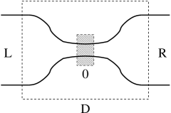
First we divide the system under study into 3 parts: The left lead (L), the right lead (R), and the intermediate region called device (D) from now on, where only elastic scattering takes place. Figure 1, shows a sketch of a nano-constriction connecting two bulk leads.
We assume that the leads are coupled only to the constriction but not to each other. The Hamiltonian describing this situation is then given by the matrix
| (1) |
Since many density functional theory (DFT) codes work in non-orthogonal basis sets, we also allow explicitly for overlap between atomic-orbitals given by the following overlap matrix:
| (2) |
The standard approach to calculate the conductance is to calculate the self-energies of the leads from the Green’s functions of the isolated leads, i.e., for the left lead where is the Green’s function of the isolated left lead and analogously for the right lead. From this we can calculate the Green’s function of the device:
| (3) |
which, in turn, allows us to calculate the (hermitian) transmission matrix
| (4) |
where and . Typically the leads are only connected to the left and right borders of the device and are sufficiently far away from the scattering region so that they can be described by a bulk electronic structure. From the structure of eq. (4) it follows that only the submatrix of representing the subspace of the device immediately connected to one of the leads are non-zero. Thus the eigenvectors obtained by diagonalizing only contain the atomic orbital contributions to the eigenchannels at one border of the device region but not at the center where the resistance is ultimately determined.
To investigate the orbital nature of the eigenchannels at an arbitrary part of the device we can simply calculate the transmission matrix associated to this part. By choosing this region to be a cross-section, like that indicated in Fig. 1, current conservation guarantees that the so-calculated conductance is approximately equal to the conductance calculated from the transmission matrix of the whole device. We want to emphasize here that this is really only approximately true for a Hamiltonian beyond the tight-binding approximation since hoppings between atoms on both sides beyond the selected region are neglected. Of course this approximation becomes better the thicker the chosen cross-section is. We proceed by further subdividing the device region. The cross-section of interest will be referred to as 0 while the regions on either side will be denoted as l and r, respectively:
| (8) | |||||
| (12) |
As mentioned above we will neglect the hoppings (and overlaps) between the left and right layers outside the region of interest so we set . With this approximation the Green’s function matrix of the cross-section can be written as
| (13) |
The self-energy matrices representing the coupling to the left and right lead, and , are given by the Green’s function of the left layer connected only to the left lead and the right layer connected only to the right lead , respectively:
| (14) | |||||
| (15) |
The reduced transmission matrix (RTM) with respect to the chosen cross-section is now given by
| (16) |
with and . Diagonalizing now yields the contribution of the atomic orbitals within the cross-section to the eigenchannels.
III Results and Discussion
In the following we apply the above described method to analyze the orbital nature of the conducting channels of Ni nanocontacts which have recently attracted a lot of interest because of their apparently high magnetoresistive properties Ni-experiments . We consider the nanocontact to consist of two ideal pyramids facing each other along the (001) direction and with the two tip atoms being 2.6 Å apart. Bulk atomic distances (2.49 Å) and perfect crystalline order are assumed for each pyramid. Just as in our previous work on Ni nanocontactsJacob et al. (2005) we perform ab initio quantum transport calculations for this idealized geometry. To this end we use our code ALACANT (ALicante Ab initio Computation Applied to NanoTransport). The electronic structure is computed at the DFT local spin density approximation level with a minimal basis set and the electrodes are described by means of a semi-empirical tight-binding Bethe lattice model.
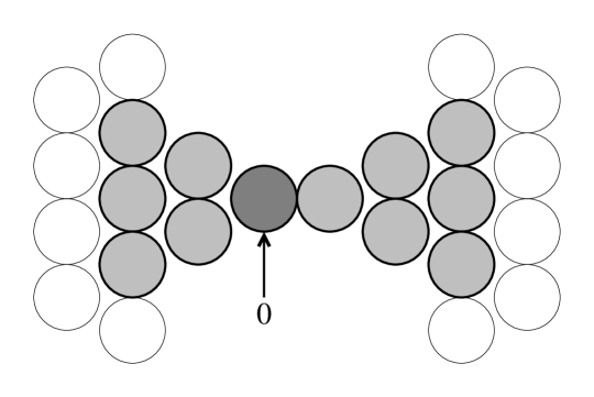
As indicated in Fig. 2 we calculate the RTM for one of the tip atoms of the contact (labelled with 0) and diagonalize it to obtain the eigenchannels and the corresponding transmissions projected on the tip atom. In Fig. 3 we compare the individual channel transmissions calculated on the one hand from the full transmission matrix (FTM) and on the other hand from the RTM . Though the electron hopping between regions l and r of the contact has been neglected in calculating the RTM the so calculated channel transmissions approximate very well those calculated using the FTM so that it is very easy to relate the RTM channel transmissions with the FTM channel transmission. This shows that the hopping between the regions l and r on both sides of the tip atom is almost negligible. Only for the one majority (M) channel we see a small deviation near the Fermi energy indicating that here 2nd neighbour hopping contributes to the transmission of that channel. As the eigenvectors of the RTM (see Table 1) reveal, this channel is mainly s-type. Since s-electrons are strongly delocalized there is a small but finite contribution from second-neighbour hopping explaining the deviation between the FTM and RTM transmission in that channel. The first minority (m) channel is also mainly s-type but now it is hybridized with and orbitals. The other two m channels are degenerate and mainly - and -type strongly hybridized with - and -orbitals, respectively.

| AO | majority | minority 1 | minority 2 | minority 3 |
|---|---|---|---|---|
| s | 97% | 62% | 0 | 0 |
| 0 | 0 | 28% | 0 | |
| 0 | 0 | 0 | 28% | |
| 3% | 23% | 0 | 0 | |
| 0 | 15% | 0 | 0 | |
| 0 | 0 | 72% | 0 | |
| 0 | 0 | 0 | 72% | |
| 0 | 0 | 0 | 0 | |
| 0 | 0 | 0 | 0 |
As discussed in our previous workJacob et al. (2005) the five d-type transport channels for the m electrons available in the perfect Ni chainSmogunov et al. (2002) are easily blocked in a contact with a realistic geometry like that in Fig. 2 because the d-orbitals are very sensitive to geometry. We have refered to this as orbital blocking. It is not so surprising that the - and -channel which are very flat bands just touching the Fermi level in the perfect chain are easily blocked in a realistic contact geometry. These bands represent strongly localized electrons which are easily scattered in geometries with low symmetry. Interestingly, even the -channel, which for the perfect chain is a very broad band crossing the Fermi level at half band width, does not contribute to the conduction as our eigenchannel analysis shows. This channel is blocked because the -orbital lying along the symmetry axis of the contact is not “compatible” with the geometry of the two pyramids. On the other hand the - and -channels are both open in that geometry because their shape is compatible with the pyramid geometry of the contacts. This illustrates how the geometry of a contact can effectively block (or open) channels composed of very directional orbitals. Of course, for different geometries we can expect different channels to be blocked or opened.
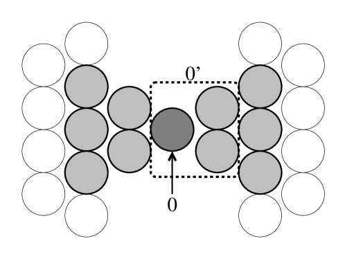
Obviously, the approximation made in the calculation of the RTM becomes worse the bigger the hopping between the regions l and r is. For example, in the contact geometry shown in Fig. 4 electron hopping from the layers immediately connected to the central atom (labeled 0) is certainly bigger than in the geometry of Fig. 2. Indeed, Fig. 5 shows that for almost all channels the RTM transmissions differ appreciably from FTM transmissions, making it difficult in some cases to relate them to each other. Fortunately, we can judge by exclusion which RTM transmission relates to which FTM transmission since for the other channels at least the RTM transmission function mimics the overall behaviour of the FTM transmission function. However, for more complicated situations it might be impossible to match the RTM transmission with the FTM transmission for all channels. The cure to this problem is obvious: One has to choose a bigger cross-section, i.e., add an atomic layer to the cross-section so that the hopping between l and r becomes small again. If we choose, e.g., the cross-section labeled with 0′ in Fig. 4 (including the atomic layer to the right of the central atom) the so calculated RTM transmissions now approximate very well the FTM transmissions as can be seen in Fig. 5.


IV Conclusions
In summary, we have shown how to obtain the orbital contributions to the eigenchannels at an arbitrary cross-section of a nanoscopic conductor. The method has been implemented into our ab initio quantum transport program ALACANT and we have illustrated the method by exploring the orbital nature of the eigenchannels of a Ni nanocontact. The method works very well when the chosen cross-section is thick enough so that hopping from the layers left and right to the cross-section becomes negligible. Hence in some cases an additional atomic layer has to be included to the cross-section we are actually interested in. Taking this into account the method has no limitations and can be readily applied to ab initio transport calculations in all types of nanocontactsFernández-Rossier et al. (2005) and molecular junctions.
Acknowledgements
We thank J. Fernández-Rossier and C. Untiedt for fruitful discussions. DJ acknowledges financial support from MECD under grant UAC-2004-0052. JJP acknowledges financial support from Grant No. MAT2002-04429-C03 (MCyT) and from University of Alicante.
References
- (1) N. D. Lang, Phys. Rev. B 52, 5335 (1995); K. Hirose and M. Tsukada, Phys. Rev. B 51, 5278 (1995); M. DiVentra, S. G. Kim, S. T. Pantelides, and N. D. Lang, Phys. Rev. Lett. 86, 288 (2001); G. Taraschi, J. L. Mozos, C. C. Wan, H. Guo, and J. Wang, Phys. Rev. B 58, 13138 (1998); N. Kobayashi, M. Brandbyge, and M. Tsukada, Phys. Rev. B 62, 8430 (2000).
- (2) P. S. Damle, A. W. Ghosh, and S. Datta, Phys. Rev. B 64, 201403(R) (2001); J. Taylor, H. Guo, and J. Wang, Phys. Rev. B 63, 245407 (2001); J. J. Palacios, A. J. Pérez-Jiménez, E. Louis, and J. A. Vergés, Phys. Rev. B 64, 115411 (2001); J. J. Palacios, A. J. Pérez-Jiménez, E. Louis, E. SanFabián, and J. A. Vergés, Phys. Rev. B 66, 035322 (2002); M. Brandbyge, J. L. Mozos, P. Ordejón, J. Taylor, and K. Stokbro, Phys. Rev. B 65, 165401 (2002); Y. Xue and M. A. Ratner, Phys. Rev. B 68, 115406 (2003); K. S. Thygesen and K. W. Jacobsen, Phys. Rev. Lett. 91, 146801 (2003); A. Bagrets, N. Papanikolaou, and I. Mertig (2005), cond-mat/0510073; V. M. Garcia-Suarez, A. R. Rocha, S. W. Bailey, C. J. Lambert, S. Sanvito, and J. Ferrer, Phys. Rev. B 72, 045437 (2005).
- (3) J. A. Torres and J. J. Sáenz, Phys. Rev. Lett. 77, 2245 (1996); M. Brandbyge, N. Kobayashi, and M. Tsukada, Phys. Rev. B 60, 17064 (1999).
- Cuevas et al. (1998) J. C. Cuevas, A. L. Yeyati, and A. Martín-Rodero, Phys. Rev. Lett. 80, 1066 (1998).
- Datta (1995) S. Datta, Electronic transport in mesoscopic systems (Cambridge University Press, Cambridge, 1995).
- Khomyakov et al. (2005) P. A. Khomyakov, G. Brocks, V. Karpan, M. Zwierzycki, and P. J. Kelly, Phys. Rev. B 72, 035450 (2005).
- Büttiker (1988) M. Büttiker, IBM J. Res. Develop. 32, 63 (1988).
- Brandbyge et al. (1997) M. Brandbyge, M. R. Sörensen, and K. W. Jacobsen, Phys. Rev. B 56, 14956 (1997).
- Jacob et al. (2005) D. Jacob, J. Fernández-Rossier, and J. J. Palacios, Phys. Rev. B 71, 220403(R) (2005).
- Thygesen and Jacobsen (2005) K. S. Thygesen and K. W. Jacobsen, Phys. Rev. Lett. 94, 036807 (2005).
- (11) N. García, M. Munoz, and Y. W. Zhao, Phys. Rev. Lett. 82, 2923 (1999); M. Viret, S. Berger, M. Gabureac, F. Ott, D. Olligs, I. Petej, J. F. Gregg, C. Fermon, G. Francinet, and G. LeGoff, Phys. Rev. B 66, 220401(R) (2002).
- Smogunov et al. (2002) A. Smogunov, A. D. Corso, and E. Tosatti, Surf. Sci. 507, 609 (2002).
- Fernández-Rossier et al. (2005) J. Fernández-Rossier, D. Jacob, C. Untiedt, and J. J. Palacios, Phys. Rev. B 72, 224418 (2005).