Single-hole transistor in p-type GaAs/AlGaAs heterostructures
Abstract
A single-hole transistor is patterned in a p-type, C-doped GaAs/AlGaAs heterostructure by AFM oxidation lithography. Clear Coulomb blockade resonances have been observed at Thole=300 mK. A charging energy of 1.5 meV is extracted from Coulomb diamond measurements, in agreement with the lithographic dimensions of the dot. The absence of excited states in Coulomb diamond measurements, as well as the temperature dependence of Coulomb peak heights indicate that the dot is in the multi-level transport regime. Fluctuations in peak spacings larger than the estimated mean single-particle level spacing are observed.
Quantum dots implemented in GaAs heterostructures represent promising candidates for the experimental realization of quantum computation Loss98 , as well as spintronics devices Wolf01 . However, research based on electronic transport through such small conducting islands was, so far, exclusively focused on quantum dots defined on n-type GaAs heterostructures (for a review, see Kouwenhoven97 ). In this paper we report about Coulomb blockade (CB) measurements in a single-hole transistor, defined on a p-type carbon doped GaAs heterostructure.
The interest in low dimensional hole-doped systems arises primarily from the fact that spin-orbit as well as carrier-carrier Coulomb interaction () effects are more pronounced in such systems compared to the more established electron-doped systems. The main reason for this is that holes have much higher effective masses than electrons, and thus a smaller Fermi energy. This should allow the investigation of novel regimes with much higher interaction parameter .
However, stronger spin-orbit interaction in hole-doped systems significantly reduces spin relaxation times in bulk p-doped GaAs systems. It was also shown Schneider04 that spin relaxation of holes confined into quantum wells is much slower than in the bulk case, but still several orders of magnitude faster than electron spin relaxation. This was one of the main reasons why hole systems received little attention in efforts to utilize spin in quantum information technologies. Recently, Bulaev and Loss predicted Bulaev05 , that further confinement of holes into quantum dots can significantly increase the relaxation time of hole spins, so that it can be comparable, or even larger than that of electron spins.
Another reason why low-dimensional hole systems have received less attention is due to technological difficulties to fabricate stable p-type structures. Nanodevices fabricated on p-type GaAs with conventional split-gate techniques show significant gate instabilities Zailer94 . This is presumably due to the fact that metallic Schottky barriers on p-type GaAs are more leaky than on n-type GaAs Williams . Our experience with metallic split-gates on p-type GaAs also shows that they display hysteretic behavior, making them unsuitable for high-precision tuning of the devices. Therefore, we decided to employ another technique, namely, Atomic Force Microscope (AFM) oxidation lithography Held98 ; Rokhinson02 to define nanostructures on two-dimensional hole gases (2DHG).
The crucial point for the implementation of AFM oxidation lithography technique is that the 2DHG is located close to the sample surface. In case of our heterostructure, the 2DHG resides at the interface 45 nm below the sample surface. The heterostructure itself consists of 5 nm undoped GaAs cap layer, followed by a 15 nm thick, homogeneously C-doped layer of AlGaAs, which is separated from the 2DHG by a 25 nm thick, undoped AlGaAs spacer layer. Before performing AFM lithography, the sample was characterized by standard magnetotransport measurements at 4.2 K and the following values are obtained for its density and mobility: n = 41011 cm-2, =120’000 cm2/Vs . The effective masses of the two spin-split subbands in C-doped GaAs heterostructures are and = 0.53 Grbic04 . The typical values for the interaction parameter in our system are determined to be .
It is important to mention that C acts as an acceptor on the (100) plane Wieck00 , and thus the anisotropy in the hole gas formed in this plane is significantly suppressed compared to the case of Si doped (311) heterostructures Grbic_unpubl . Thus the functionality of devices patterned on C-doped GaAs wafers as well as the interpretation of the transport experiments in these devices should not be dependent on the particular orientation of the device with respect to the wafer.
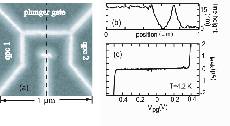
An AFM micrograph of the quantum dot is shown in Fig. 1(a). The lithographic dimensions of the dot are nm2, while the width of both quantum point contacts (qpc) is nm. The height profile in Fig. 1(b) along the dashed line in (a) indicates excellent topological homogeneity and quite constant height of the oxide lines.
We demonstrate that for a 2DHG 45 nm below the sample surface AFM written oxide lines with a height of 15-18 nm completely deplete the 2DHG beneath at 4.2 K. Voltages in the range [-500 mV, +400 mV] can be applied between separated regions without any significant leakage current across the oxide line (Fig. 1(c)). This allows us to make in-plane gates for defining nanostructures with satisfying tunability.
The transport measurements in the dot have been performed in a 3He/4He dilution refrigerator at a base temperature of 50 mK. We have measured the two-terminal conductance through the dot by applying either a small dc or ac bias voltage Vsd between source and drain, and measuring the current through the dot with a resolution better than 50 fA.
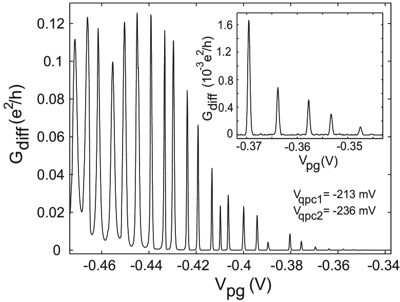
The gates qpc1 and qpc2 are tuned in the configuration Vqpc1 = -213 mV, Vqpc2 = -236 mV in which the dot is symmetrically coupled to source and drain. The differential conductance of the dot is measured as a function of the plunger gate voltage. Pronounced Coulomb resonances are observed (Fig. 2). It is important to note that the dot closes when the value of the plunger-gate voltage increases this is a clear indication that we measure hole transport. In this configuration of the gate voltages the peak positions were stable in twenty consecutive plunger-gate sweeps within an accuracy of 0.1 mV. However, it is important to mention that not every gate configuration shows such stability - in certain configurations charge rearrangements make reproducible measurements difficult.
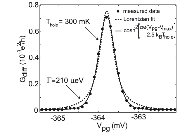
We now focus on the weak coupling regime shown in the inset of Fig. 2. Each of these five resonances is fitted both with an expression for a thermally broadened Coulomb blockade peak in the multi-level transport regime and a coupling broadened Lorentzian peak Beenakker91 (Fig. 3). In all cases the thermally broadened resonance fits significantly better to the data than a coupling broadened resonance, indicating that the dot is really in the weak coupling regime and that the peak broadening is determined by temperature rather than coupling. As a fit parameter we obtain FWHMs for each of these five peaks and they are in the range from 440 V to 480 V, which correspond to hole temperatures in the range T mK.
Coulomb diamond measurements, i.e., measurements of the differential conductance as a function of bias voltage Vbias and plunger gate voltage Vpg, are performed in the weak coupling regime, and the results are shown in Fig. 4. The uniform size of the diamonds indicates that all confined holes reside in one single potential minimum rather than occupying several disconnected or tunnel-coupled potential minima, as it was reported for a p-type SiGe quantum dot Dotsch01 . From the extent of the diamonds in bias direction we estimate a charging energy of the dot to be meV, while the lever-arm of the plunger gate is . This charging energy corresponds to a capacitance of the dot F. If we assume a disk-like shape of the dot, the capacitance is given by , where is the radius of the dot. This allows us to estimate the electronic diameter of the dot to be nm, which is in very good agreement with the lithographic dimensions of the dot and indicates that the dot is really formed in the region encircled by the oxide lines.
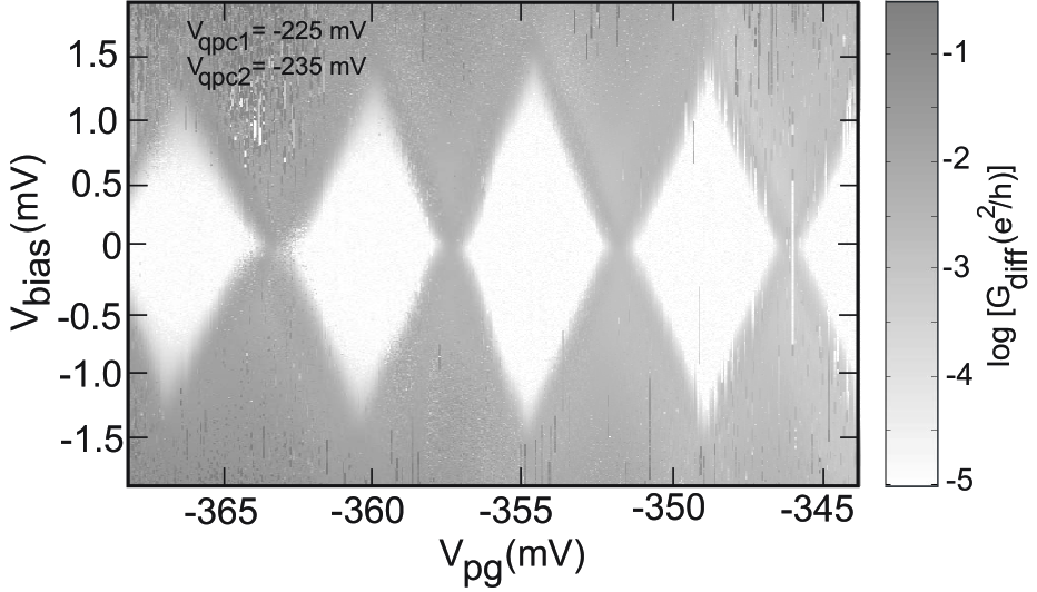
It can be seen in Fig. 4 that in certain dot configurations, low-frequency switching noise due to charge rearrangements in the sample becomes quite expressed. Although for low biases applied across the dot, the gate configurations can be found in which the switching noise in current through the dot can be completely suppressed, for large source-drain biases the switching noise becomes more pronounced and is present in almost all dot configurations.
In the case of the dot with steep potential walls, the mean single-particle level spacing can be calculated as , where is the degeneracy of hole states and is the electronic area of the dot. Due to the large effective mass of holes ( and = 0.53 ), the mean single-particle level spacing in the dot is estimated to be eV, which is one order of magnitude smaller than typical values in electron quantum dots. Since we have eV for the estimated hole temperature, the dot is in the regime where . This explains why excited states cannot be resolved in Coulomb diamond measurements.
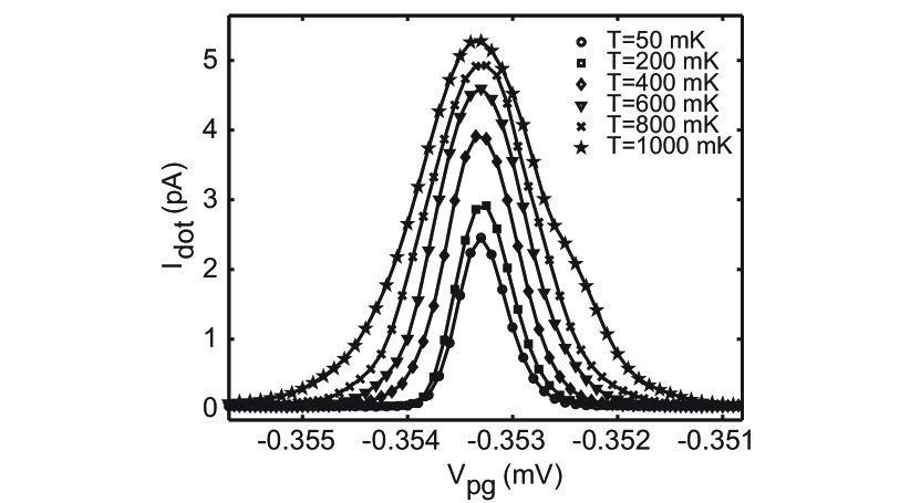
We further explored the temperature dependence of the Coulomb peaks and found that the peak amplitude does not decrease, but rather increases as the temperature increases (Fig.5). This is another indication that the dot is not in the single-level transport regime, but in the intermediate multi-level transport regime where several (about ten) single-particle levels participate in transport Kouwenhoven97 .
Despite the fact that the dot is in the multi-level transport regime, fluctuations in peak spacings are observed. The positions (in Vpg) of the five peaks shown in the inset of Fig. 2 are respectively: -369.6 mV, -363.8 mV, -357.7 mV, -353.3 mV, and -347.5 mV. Thus, the peak separations between consecutive peaks are: 5.8 mV, 6.1 mV, 4.4 mV and 5.8 mV. These fluctuations in peak separation, significantly larger than the estimated mean single-particle level spacing in the dot, may indicate some significance of stronger carrier-carrier interactions in hole quantum dots Simmel99 .
Finally, we performed a second cool-down of the same dot in another refrigerator where the thermal coupling of the sample to the mixing chamber is better. Narrower Coulomb resonances were obtained and the hole temperature extracted from the fitting of the peaks in this case was in the range T mK. This indicates, that the peak width is really determined by temperature, and that there is no intrinsic mechanism in the sample which widens the Coulomb peaks up to this energy range Dotsch01 . Eventhough the hole temperature was lower in the second than in the first cool-down, it was still not possible to resolve excited states in Coulomb diamond measurements.
In conclusion, we fabricated a quantum dot on a p-type GaAs/AlGaAs heterostructure by AFM oxidation lithography. Its functionality is demonstrated by observing clear and reproducible Coulomb resonances. From the Coulomb diamond measurements it was estimated that the charging energy of the dot is meV, which is compatible with the lithographic dimensions of the dot. However, due to the small single-particle level spacing in case of holes it was not possible to resolve excited states in the dot. In order to be able to investigate the single-particle level spectrum in hole quantum dots, one has to significantly reduce both, the lateral dimensions of the dot as well as the hole temperature. Conductance peak spacings statistics are greatly affected by interaction effects. Exploring these statistics in hole quantum dots in single-particle level regime would bring new information about the importance of carrier-carrier and spin-orbit interactions in low dimensional systems.
It’s our pleasure to acknowledge valuable discussions with R. Schleser and D. Graf concerning the AFM oxidation lithography technique and with T. Ihn and A. Gildemeister concerning the measurement setup. Financial support from the Swiss National Science Foundation, the German Science Foundation (DFG, GRK 384) and the German Ministry for Science and Education (BMBF, 01BM451) is gratefully acknowledged.
References
- (1) D. Loss and D. P. DiVincenzo, Phys. Rev. A 57, 00120 (1988).
- (2) S. A. Wolf et al., Science. 294, 1488 (2001).
- (3) L.P. Kouwenhoven et al., Proceedings of the NATO Advanced Study Institute on Mesoscopic Electron Transport, edited by L.L. Sohn, L.P. Kouwenhoven, and G. Schon, Kluwer Series E345 p. 105-214 (1997)
- (4) P. Schneider et al., J. Appl. Phys. 96, 420 (2004).
- (5) D. V. Bulaev and D. Loss, Phys. Rev. Lett. 95, 076805 (2005)
- (6) I. Zailer et al., Phys. Rev. B 49, 5101 (1994).
- (7) R. Williams, Modern GaAs Processing Methods, Artech House (1990).
- (8) R. Held, T. Vancura, T. Heinzel, K. Ensslin, M. Holland, and W. Wegscheider, Appl. Phys. Lett. 73, 262 (1998).
- (9) L. P. Rokhinson, D. C. Tsui, L. N. Pfeiffer, and K. W. West, Superl. and Microstr. 32, 99 (2002).
- (10) B. Grbić, C. Ellenberger, T. Ihn, K.Ensslin, D. Reuter, and A.D. Wieck, Appl. Phys. Lett. 85, 2277 (2004)
- (11) A. D. Wieck and D. Reuter, Inst. Phys. Conf. Ser. 166, 51 (2000).
- (12) We have tested several different C-doped (100) GaAs heterostructures in order to find the one suitable for AFM lithography. In all of these wafers the mobility anisotropy is less than 25%. This is significant improvement compared to the more established Si doped (311) wafers where the mobility along one of the main in-plain crystalographic directions is typically 2-3 times larger than in the other direction.
- (13) C. W. J. Beenakker, Phys. Rev. B 44, 1646 (1991)
- (14) U. Dötsch et al. Appl. Phys. Lett. 78, 341 (2001)
- (15) F. Simmel et al., Phys. Rev. B 59, R10441 (1999)