Acta Physicae Superficierum Vol VI 2005
ELECTRON TRANSPORT THROUGH
THE TWO-DIMENSIONAL ATOMIC LATTICE
Abstract
The electrical conductivity changes of the Si(111)-(6x6)Au surface at early stage of Pb deposition was studied experimentally and theoretically as a function of coverage. Pb deposition onto a Si(111)-(6x6)Au surface induce strong change of the conductance even at a low coverage ( monolayer). The experimental results are analyzed using the theoretical model of two dimensional (2D) square atomic lattice.
1 Introduction
The electrical conduction through semiconducting surface layer is very sensitive to the presence of individual foreign atoms. These atoms act predominantly as dopants and can, depending on the semiconductor type, enhance or decrease the electrical conductivity of the depletion or accumulation layer [1]. Presence on the semiconductor surface of a monoatomic metallic layer allows to separate these quasi two-dimensional semiconducting effects from truly two-dimensional phenomena arising during interaction of individual atoms with the surface. In this case the conventional theoretical description which takes into account the statistics of current carriers in semiconductors or the well known Drude conductivity theory, is not sufficient.
In this study we propose a theoretical model which allows to calculate the electrical conductance of truly two-dimensional lattice of atoms with single atoms deposited on it. The model simulates the initial stage of well known phenomenon of oscillating electrical resistivity observed during layer by layer growth of metallic layer [2]. The model is illustrated by experimental data of the electrical conductance of the Si(111)-(66)Au system, measured during deposition of individual atoms of Pb on it. The morphology of the surface covered with Pb atoms is studied with scanning tunnelling microscope (STM).
2 Experimental setup and results
The measurements were performed in a UHV chamber with a base pressure of less than 1x10⁻¹⁰ mbar. The structure of the substrate and the deposition of Pb were monitored by reflection high energy electron diffraction (RHEED) system. An n-type Si(111) wafer of around 25 cm resistivity and 18x4x0.4 mm3 size was used as substrate. Electrical conductivity was measured in situ by four-point probe method. An alternating current: I = 2 A, 17 Hz was sent through the outer-most Ta clamps contacts, while the ac voltage was measured across the inner two W wires kept in elastic contact with the wafer. Before each measurement run, the surface was cleaned to obtain a clear Si(111)-7x7 RHEED pattern, by few flash heating. In order to prepare the Si(111)-(6x6)Au surface structure, 1.3 ML of Au were deposited on Si(111)-7x7 superstructure. Annealing for 1 min at about 950 K and slow cooling to room temperature (10K/min.) resulted in the appearance of a sharp (6x6)Au superstructure RHEED pattern. During deposition of Pb the sample was kept at 78 K. The conductance could be measured simultaneously with deposition. The amount of deposited material in units of monolayer (ML = 7.8x10¹⁴ atoms/cm2) was monitored with a quartz crystal oscillator.
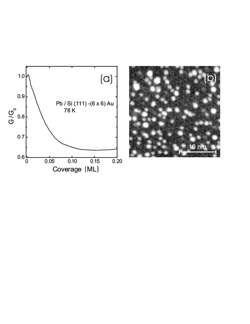
Fig.1a shows the relative conductivity changes during Pb deposition at 78 K onto a Si(111)-(6x6)Au surface for coverage up to 0.2 ML. The decrease of the conductivity starts from the beginning of the deposition. The conductivity reaches a minimum at around 0.12 ML coverage and afterwards it increases. An abrupt increase of the conductivity at opening of the shutter is connected with an influence of radiation from evaporator. The samples studied with the STM were prepared in similar condition in another UHV system equipped with Omicron VT STM. Pb films of various thickness have been deposited on such prepared substrates mounted in the cooled STM stage. During the deposition the substrate temperature was equal to about 100 K. The pressure of the chamber during the Pb deposition was below mbar. Fig. 1b shows STM scan taken after deposition of about 0.05 ML of Pb. Previous STM studies revealed [3] that at this coverage the visible small features are predominantly single Pb atoms. A few larger and brighter species are probably composed of more than single atom. The density of these atom clusters increased with Pb coverage and finally, for coverage corresponding to 1 ML of Pb(111), the whole surface was covered with epitaxial monoatomic layer of Pb.
3 Theoretical description and results
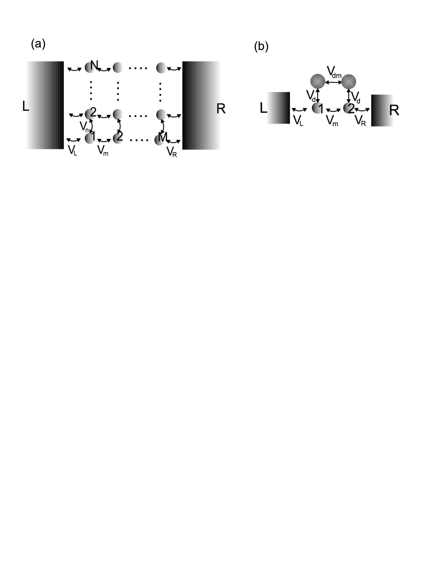
In this section we study theoretically the conductance through a model of two-dimensional (2D) square atomic lattice. The model is schematically shown in Fig. 2a. The central region, between the left (L) and right (R) electron reservoirs, consists of an array of atom sites. Additional atoms (adatoms) are added on the top of 2D lattice and cause the disturbance of the electron transport through the system. A group of coupled adatoms can be treat as a cluster of atoms. The 2D lattice of atoms is considered as the effective substrate which corresponds to, used in the experiment, Si(111)-(6x6)Au substrate. The additional atoms correspond to deposited Pb atoms and the left and right leads represent the voltage electrodes. We assume here, that each adatom is coupled only with the single substrate atom. Moreover, 3D island growth is not considered.
The total tight-binding Hamiltonian for the system can be decomposed as where describes electron states in the left and right electrodes, in the substrate and also interactions between substrate atoms. The adatom single electron states are described by the Hamiltonian . concerns adatom-adatom and substrate atom-adatom interactions. For simplicity, a single orbital per atomic site is considered. Only nearest-neighbor interactions are taken into account. We consider the total Hamiltonian in standard second-quantized notation in the following form:
| (1) | |||||
| (2) | |||||
and . Here the operators , are the annihilation (creation) operators for the reservoirs conduction electron with the wave vector , (). represents the annihilation (creation) operators for the electrons localized on the substrate atom (, ) and on adatoms above substrate atom. and are the single electron energy levels of the substrate atoms and adatoms, respectively. The elements are the hybridization matrix elements responsible for electron transport between corresponding substrate atoms and electrodes; between the lattice atoms; between adatoms and - between adatom and the 2D lattice atom. The function in the Hamiltonian is equal to if there is an additional atom at site . Otherwise it is equal to zero. This function allows to control number of adatoms included into calculations. Note, that the first term in Eq. 2 describes the interaction between the adatom and the substrate atom at site .
Electron and transport properties are analyzed within the framework of the Green’s function technique. In the energetic representation Green’s function satisfies the following equation of motion [4]:
| (3) |
Here is the energy and represents the corresponding atomic site. The knowledge of the appropriate Green’s function allows to obtain the electron local density of states (LDOS) of the substrate atoms or adatoms, i.e. for the site one can write: . The zero-temperature linear conductance, obtained for zero or very small voltage, is given in terms of the Green function by the following expression: , where is the transmittance of the system. The matrix is expressed as follows: , where . Here is the effective bandwidth of the left lead density of states. The similar expression we can write for matrix, i.e. . Using above relations the conductance of the system becomes:
| (4) |
Note, that the conductance is expressed only by the Green’s functions between atoms in the first and the last column, cf. Fig. 2a (adatoms are not connected to the leads). The appropriate Green functions are obtained using Eq. 3 and the Hamiltonian. The general matrix equation for can be written in the form: , where is the unit matrix. For the substrate atoms the matrix is expressed as follows:
and similar for the adatoms. The retarded Green functions are obtained by finding the inverse of the matrix , i.e. .
Next, we apply the above formalism to the case of two-atom lattice connected to the left and right leads and two adatoms as shown Fig. 2b. This simple model allows to study the influence of the couplings between adatoms and also between these atoms and the substrate atoms on the LDOS and conductance through the system. We treat the Fermi energy of the system as the reference energy point i.e. (the linear conductance is obtained for the left and right chemical potentials equal to the Fermi level, ), and take into consideration the case of . Moreover, the same electron energy of all substrate atoms and adatoms are assumed i.e. , . This assumption is quite reasonable as only linear regime is considered. All energies are given in units and the conductance in units.
The transport properties of the system are dependent on the density of states of this system. The conductance is proportional to the DOS of the substrate at the Fermi level [4]. For the considered system the matrix can be written in the form:
| (10) |
By calculating the inverse of the matrix we find the appropriate Green’s function needed to obtaining the LDOS. For the sake of symmetry of the system the LDOS of the substrate atoms and adatoms are equal, i.e. and - the indexes 1 and 2 (3 and 4) correspond to the substrate atoms (adatoms).

The influence of the coupling between adatoms, , on the LDOS of the substrate atoms is presented in Fig. 3. The dashed line corresponds to the case - no interaction between adatoms and the substrate atoms. The others curves correspond to the coupling between adatoms: - solid, dotted, dotted-thick lines and . The electron energy levels are and (we assume that the adatom level, in comparison to the substrate-atom level, possesses the higher energy because the ionization energy of Au is greater then for Pb atom). The dashed curve possesses two maxima for which is known behaviour of atomic wires e.g. [5]. The additional atoms blockade the LDOS around the adatom energy level , cf. the solid line. For increasing value of the coupling the LDOS dip broadens (not shown here). However, for nonzero coupling strength between adatoms the LDOS increases in the regime of energies around the Fermi energy (so about and ) - cf. the dotted lines in Fig. 3. It causes that the conductance of the system increases with increasing .
The main conclusions from this simple model are: (i) non-coupled adatoms on the 2D lattice cause decreasing of the LDOS of the substrate (and also the conductance) obtained for the Fermi energy while (ii) the adatoms which are coupled with each other cause increasing of the LDOS at the Fermi level (so the conductance through the system is greater then for non-coupled atoms in the cluster).
Now we take into consideration the system of the two-dimensional substrate of atoms and adatoms deposited on it. A series of calculations were performed for the system with increasing number of adatoms. These adatoms are placed on the lattice randomly and the conductance is obtained numerically.

Fig. 4 shows the relative conductance ( is the conductance of the substrate without adatoms) for the lattice of atoms: (left panel), 14 (middle panel), 20 (right panel) versus the coverage of the substrate. The lines are plotted for better visualization and only the coverage of order is considered as the time computation increases very strongly with increasing number of atoms in the system. For greater number of atoms in the 2D lattice the greater number of points is observed (each cross corresponds to one adatom deposited on the substrate). At the beginning the conductance decreases with increasing coverage of the substrate. This is due to the single atoms deposited on the lattice (cf. also Fig. 3). However, for the substrate coverage about 0.12 ML, the conductance possesses the local minimum. In that point the first cluster of adatoms appears and for greater coverage more clusters are observed. These clusters are responsible for increasing the conductance although there is no percolation between the left and right electrodes. This effect is also visible in Fig. 3 for the one-dimensional case. Note, that the results presented in Fig. 4 could be somewhat different for various distribution of the addatoms on the substrate. But it was checked that the general results remain unchanged.
To conclude, the theoretical results show that the conductance of 2D atomic lattice decreases with increasing coverage. For greater coverage (ML), due to clusters of adatoms, the local minimum in the conductance appears. These results are in good agreement with the experiment described in the second section and also with the STM measurements. Due to the simple theoretical model the results presented in this section should be considered only as the qualitative conclusions.
Acknowledgements
The work is partially supported by the 2004 UMCS Grant and the Foundation for Polish Science.
References
- [1] S. Hasegawa, X. Tong, S. Takeda, N. Sato and T. Nagao, Prog. Surf. Sci. 60 (1999) 89
- [2] M. Jałochowski, E. Bauer, Phys. Rev. B 37 (1988) 8622
- [3] M. Jałochowski, Progr. Surf. Sci. 74 (2003) 97
- [4] S. Datta Electonic transport in mesoscopic systems (Cambridge Univ. Press, 1995)
- [5] F. Yamaguchi, T. Yamada, Y. Yamamoto, Solid State Commun. 102 (1997) 779