Construction of a Cantilever-Andreev-Tunneling rig and its applications to superconductors
Abstract
A technique for point-contact spectroscopy, based on an electro-mechanical mechanism for the contact formation, has been developed. It is designed to be used in both 4He and 3He cryostats. The performance has been demonstrated by conductance measurements on various kinds of superconductors, including the conventional superconductor Nb, the two-band superconductor MgB2, and the heavy-fermion superconductor CeCoIn5. Characteristic conductance spectra obtained prove this technique is useful for the investigation of the superconducting order parameter. Advantages of this technique such as its simplicity and versatility are described.
pacs:
74.50.+r, 74.45.+c, 74.70.Tx, 74.20.RpI Introduction
Investigation of the order parameter symmetry and the pairing mechanism is of fundamental importance to understand the physics of superconductors. Tunneling spectroscopy, which utilizes the quantum mechanical tunneling of quasi-particles (QPs) across a tunneling barrier between a normal metal (N) and a superconductor (S), has been widely and successfully adopted to study both conventionalwolf85 and unconventional superconductors.zasadzinski03 Andreev reflection (AR) spectroscopy has also been playing an important role. This technique relies on the Andreev reflection process where the retro-reflection of a QP occurs uniquely at an N/S interface.andreev64 Blonder, Tinkham, and Klapwijk (BTK)btk82 formulated a successful theory to describe the transitional behavior from tunneling to AR as the strength of the tunnel barrier becomes smaller. There have been many extended or modified versions of the BTK theory. For instance, Tanaka and Kashiwayakashiwayatanaka extended the BTK theory to -wave superconductors.
Point-contact spectroscopy (PCS) is a technique used to investigate the electronic transport in nano-scale junctions. The BTK theories have been providing solid foundations for the analysis of PCS data obtained on superconductors.blonder83 In particular, since the recent discovery of superconductivity in MgB2,nagamatsu01 PCS has been playing a central role in defining and extracting information on the two energy gaps.szabo01 ; gonnelli02 With the simplicity of implementation, PCS has proved to be a useful tool not only to probe the superconducting order parameter but also to investigate bosonic spectrum for the pairing.jansen80 ; duif89 ; naidyuk05
In order to provide spectroscopic information, the point contact should be in a ballistic (or Sharvinsharvin65 ) limit, i.e., smaller than the electronic mean free paths of either of the contact materials. Depending on the kind of superconductors of interest and the available experimental setup, various techniques to make ballistic contacts have been developed,jansen80 ; duif89 ; naidyuk05 including thin films,yanson74 the spear-anvil technique,jansen77 pressed In contacts or Ag paint drops,gonnelli02 and scanning tunneling microscopy (STM).hawley86 Each technique has unique advantages and disadvantages. The most common technique is the use of a differential screw,blonder83 that uses fine mechanical control. This has been adopted extensively since it is straightforward and easy to implement in a cryostat. However, it has the disadvantages of mechanical backlash and difficulty in application to 3He or dilution refrigeration systems.
Because certain superconductors such as heavy-fermion superconductors (HFS) have low Tcs, requiring low temperature measurements, it is necessary to develop a PCS technique applicable in 3He or dilution refrigeration systems.goll93 ; heil93 Because of our interest in a new family of HFS, CeMIn5 (M=Co, Rh, Ir), we have developed a new technique for PCS to be used with a 3He cryostat. The probe, coined as a Cantilever-Andreev-Tunneling (CAT) rig, is also designed to be used in a liquid 4He system. In the following, we describe the design and construction of the CAT rig and present applications to three different kinds of superconductors: Nb, MgB2, and CeCoIn5.
II Design and construction of the CAT rig
The CAT rig is designed to be attached to either a 3He cryostat or a 4He probe. It is also designed to be used in two modes: Andreev reflection and planar tunneling. In the planar tunneling mode, the tunneling conductance is measured by bringing a normal-metal electrode, flattened and coated with a thin robust insulating layer, into contact with the superconductor. This technique is useful for tunneling into superconductors on which planar tunnel junctions are not easily fabricated. However, since it is not trivial to establish a technique for preparing such a counter-electrode, this mode has not yet been realized. The Andreev reflection or point contact mode is easier to implement, since one only has to fabricate a fine tip and to bring it onto the sample surface. For those reasons mentioned in the previous section, we decided to build a rig based on a two-step electro-mechanical approach, that is, a combination of a coarse approach using a screw mechanism and a fine adjustment using piezoelectric bimorphs.
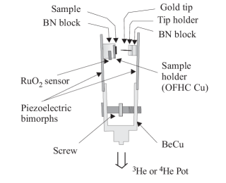
A schematic of our CAT rig is shown in Fig. 1. The body is made of BeCu to ensure enough elasticity for reversible movement of the tip and the sample. It has two arms, with a piezoelectric bimorph attached to the end of each arm. This part is finely machined to be slant to ensure that the sample surface can be aligned parallel to the surface of the counter-electrode when the contact is made in the planar tunneling mode. The piezoelectric bimorphs with nonmagnetic electrodes are driven by a linear power amplifier with a maximum output of 200 V. The input for the power amplifier is provided either by the DAC output of a lock-in amplifier or by the 20-bit DAC board. The former is used for the point contact mode since the 12-bit resolution is sufficient. The latter input is required for the planar tunneling mode to obtain more precise control of the tip-sample distance. In this case, combining the maximum deflection (325 m at room temperature and 1/7-1/8 of this value at 4.2 K chen93 ) and the resolution of the DAC (19.1 V), the ultimate resolution for the control of the tip-sample distance is estimated to be 1.4 Å at room temperature and 0.2 Å at 4.2 K. In principle, it is therefore possible to achieve control fine enough for the planar tunneling mode. A boron nitride (BN) rod is machined into rectangular and cylindrical blocks to provide electrical isolation for the sample and the tip holders from the piezoelectric bimorphs. These BN blocks are glued onto the piezoelectric bimorphs using a low temperature epoxy. The tip holder is made of aluminum and machined to screw into the cylindrical BN block. A tip is fastened to the holder by a set screw. Two copper wires are soldered to the tip holder to provide electrical leads. An OFHC Cu plate is the sample holder and is mounted on the BN block with epoxy. Four electrodes are also embedded in this BN block with epoxy. When used in the 3He cryostat, the sample holder is thermally anchored by multiple pairs of twisted Cu wires to the 3He pot to ensure good thermal conduction. The temperature of the sample is monitored with a RuO2 temperature sensor embedded into the BN block using N-grease.
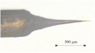
Procedures for fabricating fine gold tips to be used in STM and PCS have been well established.chen93 ; libioulle95 Figure 2 shows an optical microscope image of a gold tip prepared using an electrochemical etching technique.libioulle95 The etching of gold occurs via reduction-oxidation reactions aided by bias in an acid solution.ren04 For the best performance in PCS, the procedure is optimized to produce a thin, long, smooth, uniform and clean gold tip, as shown in Fig. 2. A long, thin tip is required because good conductance data are obtained when the tip is bent to make a contact.blonder83 The tip is fabricated from a high-purity (99.9985%) gold wire of 500 m diameter and 7-8 mm length, which acts as the anode. A thin platinum plate acts as the cathode in the HCl solution. A 5 kHz pulse of 10 V and 10 s duration is applied between them. The HCl solution of normality 12.1 is heated to 50-70 ∘C to facilitate the reaction. Right after etching is finished, the tip is rinsed thoroughly with hot deionized water to remove salts such as AuCl. The smoothness of surface is important to avoid forming multiple contacts and contamination by carbon.ren04
III Experimental Details
In this section, we describe detailed procedures for making measurements using the CAT rig in a point contact mode. Since it is designed to fit to both 3He and 4He cryostats and the procedures differ, we consider each case separately. In general, the 4He system is much easier and simpler to use. After describing the mounting of the sample and cool-down procedures in each cryostat, we describe how we monitor the sample-tip contact resistance during the cool-down procedure.
III.1 4He system
The detailed procedure for making contacts to the sample when used with 4He cryostat is as follows. The CAT rig is attached to a probe before the sample and the tip are mounted. The sample is then mounted on the sample holder using N-grease (see Fig. 1). For the measurement of conductance, two electrical leads are attached to the superconductor using Ag paint. The gold tip is used as the counter-electrode. After the sample and the tip are mounted, a contact is formed by adjusting the screw while being observed via an optical microscope. Typically, good conductance data are obtained when the tip is bent to make a contact.blonder83 This is presumably because it makes the contact more stable. Once a contact is formed, the protective cover made of OFHC copper sheet is loaded around the CAT rig.
The probe is carefully lifted and then slowly inserted into the variable temperature insert (VTI) (see Fig. 3), which has been kept above 100 K. An abrupt thermal shock to the probe must be avoided at all times. After the probe is inserted completely, the initial status of the contact is checked by measuring the zero-bias conductance (ZBC) using the standard four-probe lock-in technique. If the resistance of the contact is too high, the piezoelectric bimorphs are driven to apply more pressure. Once the contact is confirmed to be stable, the temperature is slowly lowered by opening a needle valve between the liquid 4He reservoir and the sample space. At the same time, the driving voltage to the piezoelectric bimorphs is gradually increased to ensure a stable contact and any change of the ZBC is monitored by computer. When the temperature is close to Tc, the ZBC as a function of temperature is measured continuously with decreasing temperature. The temperature is controlled by adjusting the needle valve opening and the 4He pressure.
III.2 3He system
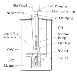
The detailed procedure for making contacts to the sample when used with the 3He cryostat is as follows. The sample and the gold tip are mounted as described in the previous section. The CAT rig is attached to the 3He cryostat which is fixed horizontally to a rigid frame. As described previously, the sample holder is thermally anchored to the 3He pot using multiple pairs of twisted Cu wires. After the contact is formed using the mechanical screw, the frame holding the cryostat is carefully lifted to a vertical position and a vacuum can is attached to the 1 K stage using a silicone sealant. We stress that this is a delicate operation and the frame is required to provide rigidity to the CAT rig while lifting, and to protect the CAT rig from any mechanical contact. After the sealant is cured for one hour, the sample space, called the inner vacuum chamber (IVC) as shown in Fig. 3, is evacuated below 50 mTorr and back-filled with 4He exchange gas to 1 Torr. Finally, the 3He cryostat is slowly inserted into the VTI. During the initial cooling down, the sorption pump heater for the 3He pot is set to near 40 K. The bias for piezoelectric bimorphs is continuously adjusted during the cool-down to ensure that the contact remains stable. When the temperatures of both the 1 K stage and the 3He pot reach 10 K, they are kept at that temperature while the 4He exchange gas in the IVC is pumped to the low 10-6 Torr range, which allows the 1 K stage to cool down further. When the temperature of the 1 K stage falls below 3 K, the 3He gas begins to condense. A complete condensation takes about 20 minutes. The sample temperature remains at around 1.2 K until the sorption pump heater power is lowered, thereby pumping on the 3He pot. A base temperature around 300 mK is typically attained. The sample temperature can be adjusted by controlling the sorption pump heater power.
III.3 Cool-down Monitoring and Bimorph Adjustment
From the shape of ZBC vs. temperature, one can identify the nature of the contact (tunneling-like, AR-like, or intermediate) by comparing the measured data with the conductance calculated using the BTK model. This information is useful to analyze and understand the conductance spectra. Once the base temperature is reached, the current vs. voltage and the conductance vs. voltage data are taken. These measurements are repeated for various magnetic fields and temperatures. The magnetic field is typically applied along the sample plane to minimize the demagnetization effect.
IV Performance and discussion
We have carried out PCS measurements on three different superconductors, Nb and MgB2 using the 4He cryostat, and CeCoIn5 using the 3He cryostat.
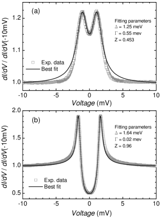
High quality Nb thin films are grown using dc magnetron sputtering in our group. Conductance spectra of two Nb thin films, deposited in different systems, are displayed in Fig. 4. The sample in Fig. 4(a) is 2100 Å thick and exhibits the Tc of 9.22 K and the residual resistivity ratio, defined as the ratio of resistivity at 300 K and at the onset temperature of the superconducting transition, of 115. The corresponding values for the sample in Fig. 4(b) are 4500 Å, 9.27 K, and 66, respectively. Fig. 4(a) and (b) can be explained in terms of different surface states of the two films. It is well known that various Nb oxides can form on the surface of as-grown Nb thin films once exposed to the air or even kept inside a vacuum chamber.lindau74 ; grundner80 Therefore, the sensitivity of Nb to oxidation may well depend on the deposition system. For most of the thin films grown in one chamber, we have observed more tunneling-like conductance curves as shown in Fig. 4(b). The Nb thin film grown in the other chamber shows more AR-like curves, as plotted in Fig. 4(a). The conductance spectra can be analyzed by the BTK model using the three fitting parameters; the energy gap , the QP lifetime smearing factor ,dynes78 and the effective barrier strength . The best fit curves are plotted as solid lines, and the fitting parameters, , , and for Fig. 4(a), and , , and for Fig. 4(b). These results clearly show that the effective barrier strength is larger in (b). The Fermi velocities in Nb and Au are well matched,ashcroft76 which means the lower limit of is nearly zero.blonder83 Thus, finite values of can be attributed to the tunnel barrier layers on the surface. The energy gap for Fig. 4(a) is 0.25 meV smaller than 1.5 meV, the value for a bulk Nb. We also note that the fit curve deviates from the measured data above 2 mV. These results may be attributed to the proximity effect,pe however, a detailed study is required to understand this behavior completely. Note also that the energy gap for Fig. 4(b)is 0.14 meV larger than the literature value. This observation is not unusual and we stress that Nb can have different superconducting properties depending on the cleanness of the material.niobium
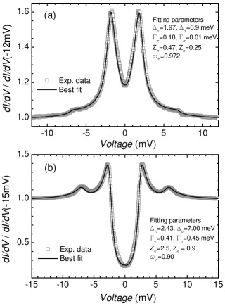
MgB2 has drawn great deal of attention due to fundamental interest and application potential. It is recognized as the first superconductor which distinctly exhibits two gaps, as shown by a variety of different experimentsszabo01 ; gonnelli02 ; bouquet01 ; iavarone02 with supporting theories.liu01 ; choi02 The point-contact spectra in Fig. 5(a) and (b) were taken on MgB2 thin films grown at the Pennsylvania State University (PSU) and at Superconductor Technology Inc. (STI), respectively. Both films are grown epitaxial with the -axis normal to the substrates. Tcs are 40.5 K and 39.3 K for the PSU and STI films, respectively. Two peaks are seen in the conductance curves, reflecting two energy gaps in agreement with the literature. Similar to Nb thin films, the two MgB2 samples show different characteristics: the conductance curve in Fig. 5(a) is more AR-like and that in Fig. 5(b)is more tunneling-like in nature. Again, this behavior can be attributed to different states on the film surface, depending on the film growth techniques. MgB2 is known to be an -wave superconductor with strong electron-phonon coupling.liu01 ; choi02 The Cooper pair condensates form on two disparate Fermi surfaces from three dimensional - and two-dimensional -bands.liu01 ; choi02 ; kortus01 Unless the interband scattering is strong, the conductance data can be analyzed using a two-band BTK model with the total conductance given by the sum of contributions from each band. In this case, there are seven fitting parameters with a weighting factor for the -band as the seventh. The best fit curves are plotted as solid lines in Fig. 5 with the fitting parameters displayed. For the data displayed in Fig. 5(a), , , , , , , and . As expected from the -axis oriented texture of the film and the two-dimensional nature of the -band Fermi surfaces, the signature for a large gap around 7 meV is much weaker, which is confirmed by the large value of required for the best fit. For Fig. 5(b), the best fit curve is obtained using , , , , , , and . In this case, two gaps are seen more clearly and confirmed by a larger weighting factor for the -band than for the data shown in Fig. 5(a). This observation can be explained by considering the texture of the film, that is, imperfect alignment of grains along the -axis. Values we obtain for the two energy gaps are in good agreement with the literature.szabo01 ; gonnelli02 ; iavarone02

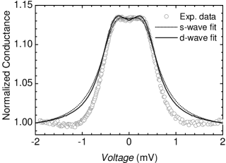
Our interest in the HFS, which have relatively low Tcs, requires a 3He cryostat or a dilution refrigerator to study their superconducting properties. In particular, we have studied CeCoIn5 well below its Tc (2.3 K) by attaching the CAT rig to the 3He cryostat. A CeCoIn5 single crystal is etched in a concentrated hydrochloric acid to remove any residual indium. The point contact between a single crystal CeCoIn5 and a gold tip is formed with the tip axis perpendicular to the crystal plane so the current is injected along the -axis. The dynamic conductance spectra, taken over a wide temperature range, from 60 K to 400 mK, are shown in Fig. 6.park05 An asymmetry in the background conductance is seen to develop starting at 40 K, which we attribute to the emergence of the coherent heavy-fermion liquid.nakatsuji04 This asymmetry is nearly constant below Tc (2.3 K), where an enhancement of the sub-gap conductance is observed. A striking feature is the flat region in the subgap conductance at lower temperatures, reminiscent of AR. From estimations of the contact size and electronic mean free paths, the contact is shown to be in the Sharvin limit.park05 Analyses based on the extended BTK modelkashiwayatanaka indicate that -wave symmetry is more likely than -wave, in agreement with the literature.thompson03 ; izawa01 ; eskildsen03 ; aoki04 However, the full conductance curves cannot be fully accounted for, as shown in Fig. 7. We claim that this failure is closely related to the heavily suppressed AR across a N/HFS interface, gloos95 ; anders97 and provide a framework for better theoretical understanding.park05
We have demonstrated that our CAT rig is a useful and reliable technique for the spectroscopic investigation of a variety of superconductors. Furthermore, the rig is stable and robust against thermal cycles. An obvious advantage of this technique is its versatility and its simplicity of implementation. We have shown it is adapted to both 4He and 3He cryostats. In addition, the tips can be exchanged so that different tip materials may be used, including ferromagnets and superconductors. An outstanding challenge remaining is the planar tunneling mode of the CAT rig.
ACKNOWLEDGEMENTS
We are grateful to C. Gulyash and S. Schultz for their excellent machining work, J. L. Sarrao and J. D. Thompson at Los Alamos National Laboratory for providing CeCoIn5 single crystals, B. Moeckly at Superconducting Technology Inc., J. M. Rowell at the Arizona State University, P. Orgiani and Q. Li at the Pennsylvania State University for providing MgB2 thin films, J. Elenewski, B. F. Wilken, K. Parkinson, A. N. Thaler, P. J. Hentges, M. K. Brinkley, C. J. Ramsey, J. B. McMinis, A. O’Brien, X. Lu, and W. L. Feldmann for their experimental help. This work was supported by the U.S. Department of Energy, Division of Materials Sciences under Award No. DEFG02-91ER45439, through the Frederick Seitz Materials Research Laboratory and the Center for Microanalysis of Materials at the University of Illinois at Urbana-Champaign.
References
- (1) E. L. Wolf, Principles of Electron Tunneling Spectroscopy, Oxford University Presss, Inc., New York, 1985.
- (2) J. Zasadzinski, in The Physics of Superconductors, edited by K. H. Bennemann and J. B. Ketterson, Springer-Verlag, Berlin, Germany, 2003.
- (3) A. F. Andreev, Zh. Eksp. Teor. Fiz. 46, 1823 (1964) [Sov. Phys. JETP 19, 1228 (1964)].
- (4) G. E. Blonder, M. Tinkham, and T. M. Klapwijk, Phys. Rev. B 25, 4515 (1982).
- (5) Y. Tanaka and S. Kashiwaya, Phys. Rev. Lett. 74, 3451 (1995); S. Kashiwaya, Y. Tanaka, M. Koyanagi, and K. Kajimura, Phys. Rev. B 53, 2667 (1996); S. Kashiwaya and Y. Tanaka, Rep. Prog. Phys. 63, 1641 (2000).
- (6) G. E. Blonder and M. Tinkham, Phys. Rev. B 27, 112 (1983); G. E. Blonder, Ph.D. thesis, Harvard University, 1982.
- (7) J. Nagamatsu et al., Nature 410, 63 (2001).
- (8) P. Szabó et al., Phys. Rev. Lett. 87, 137005 (2001).
- (9) R. S. Gonnelli et al., Phys. Rev. Lett. 89, 247004 (2002).
- (10) A. G. M. Jansen, A. P. van Gelder, and P. Wyder, J. Phys. C: Solid St. Phys., 13, 6073 (1980).
- (11) A. M. Duif, A. G. M. Jansen, and P. Wyder, J. Phys.: Condens. Matter. 1 3157 (1989).
- (12) Yu. G. Naidyuk and I. K. Yanson, Point-Contact Spectroscopy, Springer Science+Business Media, Inc., New York, 2005.
- (13) Yu. V. Sharvin, Zh. Eksp. Teor. Fiz. 48, 984 (1965) [Sov. Phys. JETP 21, 655 (1965)].
- (14) I. K. Yanson, Zh. Eksp. Teor. Fiz. 66, 1035 (1974) [Sov. Phys. JETP 39, 506 (1974)].
- (15) A. G. M. Jansen, F. M. Mueller, and P. Wyder, Phys. Rev. B 16, 1325 (1977).
- (16) M. E. Hawley, K. E. Gray, B. D. Terris, H. H. Wang, K. D. Carlson, J. M. Williams, Phys. Rev. Lett. 57, 629 (1986).
- (17) G. Goll, H. v. Löhneysen, I. K. Yanson, L. Taillefer, Phys. Rev. Lett. 70, 2008 (1993); G. Goll, Ph.D. thesis, Karlsruhe, 1993.
- (18) J. Heil, Y. de Wilde, A. G. M. Jansen, and P. Wyder, Rev. Sci. Instrum. 64, 1347 (1993).
- (19) C. J. Chen, Introduction to Scanning Tunneling Microscopy, Oxford University press, Oxford, UK (1993).
- (20) L. Libioulle, Y. Houbion, and J.-M. Gilles, J. Vac. Sci. Technol. B 13, 1325 (1995).
- (21) B. Ren, G. Picardi, and B. Pettinger, Rev. Sci. Instrum., 75, 837 (2004).
- (22) I. Lindau and W. E. Spicer, J. Appl. Phys. 45, 3720 (1974).
- (23) M. Grundner and J. Halbritter, J. Appl. Phys. 51, 397 (1980).
- (24) R. C. Dynes, V. Narayanamurti, and J. P. Garno, Phys. Rev. Lett. 41, 1509 (1978).
- (25) N. W. Ashcroft and N. D. Mermin, Solid State Physics, New York, 1976.
- (26) A. Di Chiara, F. Fontana, G. Peluso, and F. Tafuri, Phys. Rev. B 48, 6695 (1993); G. J. Strijkers et al., ibid. 63, 104510 (2001); G. Sheet, S. Mukhopadhyay, and P. Raychaudhuri, ibid. 69, 134507 (2004).
- (27) I. V. Roshchin et al., Phys Rev B 66, 134530 (2002); K. S. Ilin et al., Physica C 408-410, 700 (2004); L. H. Greene et al., Superlattice Microst. 1, 407 (1985); S. V. Vonsovsky, Yu. A. Izyumov, and E. Z. Kurmaev, pp. 188-190 in Superconductivity of Transition Metals, Springer-Verlag, Berlin, Germany, 1982.
- (28) F. Bouquet et al., Phys. Rev. Lett. 87, 047001 (2001).
- (29) M. Iavarone et al., Phys. Rev. Lett. 89, 187002 (2002).
- (30) A. Y. Liu, I. I. Mazin, and J. Kortus, Phys. Rev. Lett. 87, 087005 (2001).
- (31) H. J. Choi et al., Nature 418, 758 (2002).
- (32) J. Kortus, I. I. Mazin, K. D. Belashchenko, V. P. Antropov, and L. L. Boyer, Phys. Rev. Lett. 86, 4656 (2001).
- (33) W. K. Park, L. H. Greene, J. L. Sarrao, and J. D. Thompson, Phys. Rev. B 72, 052509 (2005); W. K. Park, L. H. Greene, J. L. Sarrao, and J. D. Thompson, cond-mat/0507353.
- (34) S. Nakatsuji, D. Pines, and Z. Fisk, Phys. Rev. Lett. 92, 016401 (2004).
- (35) J. D. Thompson et al., Physica B 329-333, 446 (2003).
- (36) K. Izawa et al., Phys. Rev. Lett. 87, 057002 (2001).
- (37) M. R. Eskildsen et al., Phys. Rev. Lett. 90, 187001 (2003).
- (38) H. Aoki et al., J. Phys.: Condens. Matter 16, L13 (2004).
- (39) K. Gloos et al., Physica B 206 & 207, 279 (1995).
- (40) F. B. Anders and K. Gloos, Physica B 230-232, 437 (1997).