theDOIsuffix \VolumeXX \Issue1 \Month01 \Year2004 \pagespan1 \Receiveddate2 September 2004
Scanning tunneling microscopy of monoatomic gold chains on vicinal Si(335) surface: experimental and theoretical study
Abstract.
We study electronic and topographic properties of the Si(335) surface, containing Au wires parallel to the steps. We use scanning tunneling microscopy (STM) supplemented by reflection of high energy electron diffraction (RHEED) technique. The STM data show the space and voltage dependent oscillations of the distance between STM tip and the surface which can be explained within one band tight binding Hubbard model. We calculate the STM current using nonequilibrium Keldysh Green function formalism.
keywords:
STM; atomic wire; vicinal surface; tunnelingpacs Mathematics Subject Classification:
68.37.Ef, 81.07.Vb, 73.40.Gk1. Introduction
Recently, the high-index (vicinal) surfaces have attracted much attention due to possibility of the creation of one dimensional structures on them [1]. On such surfaces, deposition of small amount of metal often results in the formation of the chain structures [2]-[11]. Such one dimensional wires are important from scientific point of view, as they should exhibit Luttinger liquid behavior [13, 14], as well as from technological one (nanoelectronics, quantum computing).
The examples of the one dimensional structures on vicinal surfaces are metallic wires on silicon, like: Au/Si(335) [8]-[10], Au/Si(557) [2]-[8], Au/Si(5512) [11] and Ga/Si(112) [12]. The Au/Si(335) surface consists of Si(111) terraces wide and long monoatomic chains along these terraces are observed at Au coverage [8]-[10]. For the Au/Si(557) terraces are wide and critical coverage is [8, 10].
Many techniques have been developed in surface science in order to investigate the electronic and topographic properties of such systems. Those include: angle resolved photoemission spectroscopy, low and high energy electron diffraction, x-ray diffraction. Unfortunately they provide averaged data over the sample surface and are not appropriate for very small (nanometer size) objects. One of the most powerful techniques in surface science is the scanning tunneling microscopy (STM) [15] which is extremely sensitive to the electronic structure of the topmost atomic layer of the material and allows to study properties of the objects on sub-nanometer (atomic) scale.
On the other hand there is also a couple of theoretical papers regarding STM technique, mainly in context of single impurity on surface [16, 17] and the surface itself [15]-[19]. Recently the problem of one dimensional objects on surfaces has also been raised, for example STM imaging of Luttinger liquid [20] or molecular wires [21]. The surface reconstructions of the gold nanowires on Si(557) have been investigated by Sanchez-Portal and Martin within first principle density functional theory [22]. The local density of states of Au chains on NiAl(110) surface has also been studied within the same technique [23].
In the present work we provide STM data from Au induced structures on Si(335) surface and demonstrate how the STM images depend on the tip-surface voltage, especially on its polarization. To understand this effect we propose a model of tunneling between STM tip and the surface and calculate the tunneling current within nonequilibrium Keldysh Green function formalism. Theoretical description is in a good qualitative agreement with STM experimental data. Rest of the paper is organized as follows: in Sec.2 we describe the experimental setup and provide some data. In Sec. 3 we introduce theoretical one band tight binding model and results are presented in Sec. 4. Finally we conclude in Sec. 5.
2. Experiment
Experimental setup consists of ultra high vacuum (UHV) chamber equipped with a scanning tunneling microscope (type OmicronVT) and reflection high energy electron diffraction (RHEED) apparatus. Samples were prepared in-situ and the base pressure was less than mbar during measurements. The monoatomic long wires have emerged after deposition of ML of Au and heating the sample at temperature K for s. The quality of the surface reconstruction has been controlled by RHEED technique.
In Fig. 1 we show the STM topography data of the same area of the sample taken at tunneling current nA and the sample bias V (a) and V (b).
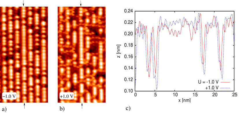
Note clear change of the images. At positive bias some bright structures are no more visible whereas the others emerge. While the mean features, namely the chain - like structure remains, the lengths of the wires and their internal structure change a little. It is clearly seen in the Fig. 1 (c), where the cross sections along atomic chains, indicated by arrows in (a) and (b), are shown. We see that upon reversing of the sample bias reverses also topography of the nanowire. The maxima change into minima and vice versa. We stress that this effect has strictly electronic origin. In order to avoid possible influence of the sample thermal drift, insensitive to the sample bias, the specific surface defect (not shown in the figure) was chosen as a reference point.
Those data clearly indicate that the electron density of states along the nanowire is strongly modulated with the periodicity, corrected by the sensitivity of the STM scanner, was equal to about . The reversal of the topography images shows that the electron density distribution between the atoms of the nanowire is opposite to the electron density distribution on it. To explain this effect we have performed calculations within tight binding model.
3. The model
Our model system is described by the Hamiltonian:
| (1) |
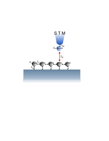
and consists of metallic wire with the site (atomic) energies and the hopping parameter between atoms. The wire is connected via parameters to the surface, which we treat as a reservoir for electrons with single particle energies . Above the wire there is a tip modeled by single atom with atomic energy attached to the another reservoir (with electron energies ) via hopping . Tunneling of the electrons between STM tip and one of the atoms in a wire is described via tunneling matrix element . As usually () stands for creation (annihilation) electron operator in STM lead (), tip atom (), wire () and surface (). Schematic view of our system is shown in the Fig. 2.
In order to calculate the tunneling current from the tip to the surface we have adapted equation of motion technique for nonequilibrium Keldysh Green functions [24, 25]. The final expression for the tunneling current through the wire containing atoms is given by:
| (2) |
where transmittance is given in the form:
| (3) |
is the coupling parameter between tip lead and tip site, and surface and wire. is the usual Fermi distribution function and () is the chemical potential of the tip (surface). is the matrix element (connecting the tip site with the wire atom ) of the retarded Green function , solution of the equation:
| (4) |
4. Results and discussion
To calculate the topography of the wire we have solved Eqs. (2)-(4) selfconsistently for given bias voltage () and fixed current and obtained value of (in units of ) which depends on the distance between the tip and the wire. In order to make comparison with experimental data we have adapted formula from Ref. [21] connecting these two quantities
| (5) |
where is the electron mass, - work function taken as eV for Si, - length parameter (order of an orbital spatial size) chosen as nm [21], and - distance between tip and the surface. In our model the wire atoms have been equally placed with the distance equal to the Si lattice constant in direction .
In Fig. 3 we show the comparison of the experimental topographic data for a wire of typical length observed in STM experiment with the theoretical calculations.
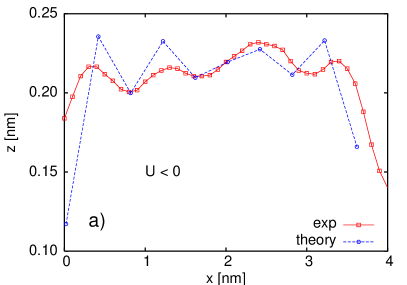
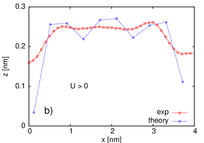
First of all it is worthwhile to note that we observe different number of minima and maxima of the distance between tip and surface for negative Fig. 3 (a) and positive (b) bias voltages. While for we have four maxima, for there are 3 such maxima. This is due to different energy distribution of the transmittance (see Eq. (3)). The transmittance as a function of energy for positive and negative sample bias is shown in the Fig. 4.
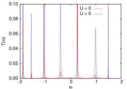
For the energy independent it is in close relation with the wire density of states. The transmittances integrated over energy together with the Fermi functions give tunneling currents and therefore different values of the distance which is in close relation with via Eq. (5). So one can say that this effect is purely of electronic nature. Similar effect, namely changes of the number of maxima and minima in the local density of states with bias voltage, has been observed in Ref. [23] for gold wires on NiAl(110) surface.
Another important effect is the period of the oscillations seen in the Fig. 3. We stress that the periodicity of the atomic chain, as expected from the Au coverage [2, 9], is equal to , whilest the observed and calculated period is equal to about . This period seems to not depend on the wire length. Moreover, to get a reasonable consistency with the experimental data, we had to modify an atomic energy of the atom at one of the ends of the wire. This indicates that wires strongly interact via surface with neighboring ones on the same terrace.
5. Conclusions
In conclusions we have studied experimentally and theoretically gold nanowires on vicinal Si(335) surface. The wires of differnent length were grown along terraces in direction at Au coverage equal to ML. The STM topographic data show strong dependence on the sample bias revealing space dependent oscillations of the distance between STM tip and surface with a period two of Si lattice constant in direction , along the chain. The period of oscillations seems to not depend on the length of the nanowires. Moreover calculations based on tight binding model indicate that those wires strongly interact with neighboring ones situated on the same terrace. The problem of interaction with the surface as well as interaction between chains on differnt terraces is under consideration and will be published elsewhere.
M. K. acknowledges a partial support by the grant no. PBZ-MIN-008/P03/2003.
References
- [1] F. J. Himpsel et al., J. Phys. Condens. Matter 13 (2001) 11097.
- [2] M. Jałochowski et al., Surf. Sci. 375 (1997) 203.
- [3] P. Segovia et al., Nature (London) 402 (1999) 504.
- [4] R. Losio et al., Phys. Rev. Lett. 86 (2001) 4632.
- [5] K. N. Altmann et al., Phys. Rev. B 64 (2001) 035406.
- [6] D. Sanchez-Portal et al., Phys. Rev. B 65 (2002) 081401.
- [7] I. K. Robinson et al., Phys. Rev. Lett. 88 (2002) 096104.
- [8] J. N. Crain et al., Phys. rev. B 69 (2004) 125401
- [9] R. Zdyb et al., Vacuum 63 (2001) 107.
- [10] J. N. Crain et al., Phys. Rev. Lett. 90 (2003) 176805.
- [11] S. S. Lee et al., Phys. Rev. B 66 (2002) 115317.
- [12] C. Gonzales et al., preprint cond-mat/0404285.
- [13] J. M. Luttinger, J. Math. Phys. 4 (1963) 1154.
- [14] F. D. M. Haldane, J. Phys. C: Solid State Phys. 14 (1981) 2585.
- [15] W. A. Hoferet al., Rev. Mod. Phys. 75 (2003) 1287.
- [16] A. Schiller, S. Hershfield, Phys. Rev. B 61 (2000) 9036.
- [17] M. Plihal, J. W. Gadzuk, Phys. Rev. B 63 (2001) 085404.
- [18] G. Hörmandinger, Phys. Rev. B 49 (1994) 13897.
- [19] S. Heike et al., J. Appl. Phys. 86 (1999) 4220.
- [20] S. Eggert, Phys. Rev. Lett. 84 (2000) 4413.
- [21] Y. Calev et al., preprint cond-mat/0403596.
- [22] D. Sanchez-Portal, R. M. Martin, Surf. Sci. 532 (2003) 655.
- [23] M. Persson, preprint cond-mat/0405675.
- [24] M. Krawiec, K. I. Wysokiński, Solid State Commun. 115 (2000) 141.
- [25] M. Krawiec, K. I. Wysokiński, Supercond. Sci. Technol. 17 (2004) 103.