Magnetoresistance of atomic-scale electromigrated nickel nanocontacts
Abstract
We report measurements of the electron transport through atomic-scale constrictions and tunnel junctions between ferromagnetic electrodes. Structures are fabricated using a combination of e-beam lithography and controlled electromigration. Sample geometries are chosen to allow independent control of electrode bulk magnetizations. As junction size is decreased to the single channel limit, conventional anisotropic magnetoresistance (AMR) increases in magnitude, approaching the size expected for tunneling magnetoresistance (TMR) upon tunnel junction formation. Significant mesoscopic variations are seen in the magnitude and sign of the magnetoresistance, and no evidence is found of large ballistic magnetoresistance effects.
pacs:
75.75.+a, 75.70.Kw, 85.70.-wMagnetoresistive effects in ferromagnetic structures are of considerable technological and scientific interest. The anisotropic magnetoresistance (AMR) results from spin-orbit scattering and is manifested as a change in resistivity, , as a function of the relative orientation of the magnetization and the current density . In Ni, . Tunneling magnetoresistance (TMR) results from the difference in majority and minority densities of states at the Fermi level. Tunneling resistance, , is generally enhanced for antialigned magnetizations of the electrodes on either side of the tunnel barrier. The magnitude of TMR in large area junctions is , where is the spin polarization at the Fermi levelJulliere55PLA .
The magnetoresistance of atomic-scale constrictions in magnetic wires has been the subject of intense interest since the initial report of large ballistic magnetoresistance (BMR) in junctions between Ni wiresGarciaetAl99PRL . Reports of BMR magnitudes far in excess of typical AMR and TMR effects have generated considerable controversy, including concerns about magnetostrictive artifactsEgelhoffetAl04JAP . It is therefore of much interest to examine constrictions fabricated in a geometry that minimizes these effects and allows temperature-dependent studies of junction magnetoresistances. Recent experiments along these lines have used mechanical break junctionsViretetAl02PRB , planar electrochemically grown junctionsYangetAl04APL , ballistic nanoporesOzatayetAl04JAP , and ion-beam-formed constrictionsMonteroetAl04PRB
In this Letter we report measurements of the magnetoresistance through few-atom and single-atom contacts between planar Ni electrodes, as well as planar Ni-Ni tunnel junctions. Junctions are fabricated by a combination of electron beam lithography and controlled electromigration. This allows the examination of individual nanostructures with junction configurations serially modified from planar films to few-atom contacts to vacuum tunnel junctions. These planar structures are chosen to minimize magnetostrictive effects, as discussed below. Small junction size is confirmed by evidence of conductance quantization and discrete switching. At 10 K, conventional AMR is observed in large junctions, and increases in magnitude as the number of channels approaches one. We observe significant sample-to-sample variation in the shape and sign of the magnetoresistance, with an upper limit on the magnitude consistent with TMR in Ni of known properties. This variability, typical of mesoscopic systems, suggests that the bulk magnetization of the electrodes is not simply related to the local magnetization of the few atoms directly relevant for tunneling.
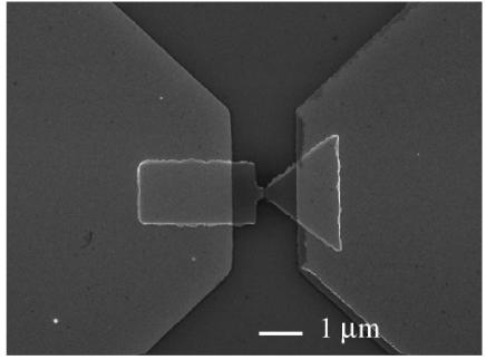
Devices are fabricated by a two-step lithography process on test grade Si wafers coated with 200 nm thermal oxide. Ni structures are defined by e-beam lithography and e-beam evaporation (20 nm thick Ni film deposited at 2 Å/s in a system with mB base pressure). This is followed by a second lithography step, Ar ion sputter cleaning to ensure good contact to the Ni layer, and evaporation of 1 nm Ti/30 nm Au leads to make electrical contact. Sample geometries, shown in Fig. 1, were chosen to minimize magnetostrictive effects by anchoring the bulk electrodes firmly to the substrate, and to create a well-defined domain structure near the constriction so that the data could be more easily interpreted. The micron scale of the Ni pads increases the likelihood that each will consist of a single domain. The electrode shapes favor controlled relative reorientation of their bulk magnetizationsJedemaetAl01Nature ; PasupathyetAl04Science . In the absence of an external magnetic field, is favored to lie in the plane of the electrodes and parallel to the current.
The Ni constrictions are progressively broken by electromigrationParketAl99APL to achieve contacts ranging from a few atoms to vacuum tunnel junctions. All measurements are performed at 10 K in a variable temperature vacuum cryostat to mitigate oxidation of the Ni atoms near the contact. The system is relatively stable at this temperature, allowing measurement of the same device in multiple configurations; in this way we were able to observe the evolution of these devices from bulk metal through the ballistic regime into the tunneling regime.
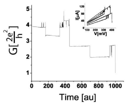
To achieve few-atom contacts and clean vacuum tunnel junctions reliably, precise control of the electromigration procedure is paramount; our procedure for nickel closely follows that previously reported for room-temperature gold nanojunctionsStrachanetAl05APL . Achieving stable few-channel junctions is extremely challenging, with a success rate of 8%. Current-voltage curves and corresponding conductance data from a successful electromigration run resulting in a 13 k device are shown in Fig. 2. The discontinuities in the last few curves, and the corresponding conductance plateaux, indicate that the device under test likely consists of a few atoms at its narrowest point. Such few-channel junctions often exhibit telegraph noise with conductance changes , also consistent with extremely narrow constrictions.
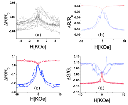
A family of magnetoresistance curves from one of these devices is shown in Fig. 3. The magnetization of the leads lies in the plane of the film until a coercive external field is applied out of plane. An in situ rotation stage allows the acquisition of magnetoresistance data as a function of field orientation for a single junction configuration. The magnetoresistance under a transverse field evolves gradually from a small AMR in the bulk to a larger, similarly-shaped curve as the device is broken into the ballistic regime. The initial magnitude of the out-of-plane MR in an unbroken starting device is typically a few tenths of a percent; while AMR in nickel films is typically 2%, the smaller value is reasonable since initially the measured resistance is dominated by the leads and wiring. As the device is progressively broken, the MR quickly approaches and then surpasses the expected magnitude for bulk AMR: in few- and single-channel devices, this effect can approach 20%. Finally, in the tunneling regime, we see fairly typical MR magnitudes for a vacuum tunnel junction, with TMR values of 10-20%. Table 1 shows several samples measured in different electromigrated configurations at 10 K.
| Sample | Resistance | Longitudinal MR [%] | Transverse MR [%] |
|---|---|---|---|
| A | 7.1 k | 0.78 | 1.14 |
| A | 83 k | 20.7 | 16.4 |
| B | 13 k | 20.5 | 8.03 |
| B | 5 M | 11.3 | 10.7 |
| C | 10 M | 9.43 | 7.07 |
| D | 13 k | 5.13 | 10.7 |
| D | 200 k | 13.3 | [not measured] |
| E | 5.8 k | 3.3 | 15.4 |
| E | 13 k | 8.69 | 21.9 |
A closer look at the curves in Fig. 3 reveals some aspects, other than the surprisingly large magnitude fo the AMR-like effect, in which the behavior of these devices diverges from traditional AMR. The most readily apparent of these unusual behaviors is the appearance of switching features at applied fields of around 2 KOe perpendicular to the current. These features are not observed in any devices prior to electromigration. The hysteretic nature of these switching features suggests that they may be due to domain reversal in the Ni metal. In both in-plane and out-of-plane field sweeps, the magnitude and sign of the TMR has significant variability from device to device.
Magnetostriction is a possible confounding effect: one need only cause a single- atom mechanical contact to shift by a fraction of a nanometer to cause a large conductance change. A recent experimentGabureacetAl04PRB designed to quantify the effects of magnetostriction in nickel mechanical break junctions indicates that, in a geometry with a 650 nm undercut beneath the bridge, magnetostriction accounted for a 40% change in the resistance of an atomic-scale contact. Magnetostriction is very unlikely to account for our results for two reasons. First, in our geometry, the Ni wires are constrained by the silicon substrate everywhere except for the immediate neighborhood of the constriction; the length of the bridge which is unconstrained by the substrate below is at most 10 nm, which should result in a much smaller magnetostrictive effect. Second, the magnetoresistance curves shown in GabureacetAl04PRB are qualitatively different from those reported here, particularly in the lack of fine structure.
The complicated MR patterns and variability indicate that domain structure in the bulk electrodes is not simply related to the atomic-scale magnetization at few-atom contact or point of tunneling. Since there is no evidence of Coulomb blockade as these devices approach the TMR limit, it is unlikely that the effects seen are a result of unintentional nanoparticle formation during electromigration. Similar variability and complicated magnetic structure has also been seen in mechanical break junction experiments in the few-channel regimeViretetAl02PRB . Such strong sensitivity to detailed contact geometry has also been supported theoreticallyJacobetAl05PRB .
Three factors are likely to be relevant to understanding these observations. First, single-molecule transistor measurements with ferromagnetic leadsPasupathyetAl04Science have explicitly demonstrated that effective exchange fields at surface atoms can be large (70 T) and different from the bulk. Second, tunneling via localized states (possibly surface states in this case) has been demonstrated to lead to inverted TMRTsymbaletAl03PRL , as have highly transmitting channelsKim05PRB . Third, it is possible that trace amounts of NiOx or unintended adsorbates at the tunneling point can cause local perturbations of the tunneling spins. Detailed atomic-scale variations in the junctions clearly can have a profound influence on relevant magnetoresistive processes.
In summary, in nanoscale Ni junctions we observe an evolution of magnetoresistance from ordinary AMR in wide junctions, to an enhanced AMR in few-channel wires, to TMR in tunnel junctions, with large sample-to-sample variability in the shapes and signs of the TMR. No magnetoresistances are observed that are larger than those expected from the known polarization of Ni. The mesoscopic variation in MR indicates that the local junction environment can have a strong affect on the spin of the tunneling carriers. Further study is required to determine the precise physics behind this effect.
We note that Bolotin, Kuemmeth, Pasupathy, and Ralph have recently posted independent results of a similar experimentBolotinetAl05 .
This work was supported by NSF NER award ECS-0403457, the David and Lucille Packard Foundation, and an Alfred P. Sloan Foundation research fellowship.
References
- (1) M. Julliere, Phys. Lett. A 54, 225 (1955).
- (2) N. García, M. Muñoz, and Y.-W. Zhao, Phys. Rev. Lett. 82, 2923 (1999).
- (3) W.F. Egelhoff, Jr., L. Gan, H. Ettedgui, Y. Kadmon, C.J. Powell, P.J. Chen, A.J. Shapiro, R.D. McMichael, J.J. Mallett, T.P. Moffat, M.D. Stiles, E.B. Svedberg, J. Appl. Phys. 95, 7554 (2004).
- (4) M. Viret, S. Berger, M. Gabureac, F. Ott, D. Olligs, I. Petej, J.F. Gregg, C. Fermon, G. Francinet, and G. Le Goff, Phys. Rev. B 66, 220401(R) (2002).
- (5) C.-S. Yang, C. Zhang, J. Redepenning, and B. Doudin, Appl. Phys. Lett. 84, 2865 (2004).
- (6) O. Ozatay, P. Chalsani, N.C. Emley, IN. Krivorotov, and R.A. Buhrman, J. Appl. Phys. 95, 7315 (2004).
- (7) M.I. Montero, R.K. Dumas, G. Liu, M. Viret, O.M. Stoll, W.A.A. Macedo, and I.K. Schuller, Phys. Rev. B 70, 184418 (2004).
- (8) F.J. Jedema, A.T. Filip, and B.J. van Wees, Nature 410, 345 (2001).
- (9) A.N. Pasupathy, R.C. Bialczak, J. Martinek, J.E. Grose, L.A.K. Donev, P.L. McEuen, and D.C. Ralph, Science 306, 86 (2004).
- (10) H. Park, A.K.L. Lim, A.P. Alivisatos, J. Park, and P.L. McEuen, Appl. Phys. Lett. 75, 301 (1999).
- (11) D.R. Strachan, D.E. Smith, D.E. Johnston, T.-H. Park, M.J. Therien, D.A. Bonnell, and A.T. Johnson, Appl. Phys. Lett. 86, 043109 (2005).
- (12) M. Gabureac, M. Viret, F. Ott, and C. Fermon, Phys. Rev. B 69, 100401 (2004).
- (13) D. Jacob, J. Fernández-Rossier, and J.J. Palacios, Phys. Rev. B 71, 220403(R) (2005).
- (14) E.Y. Tsymbal, A. Sokolov, I.F. Sabirianov, and B. Doudin, Phys. Rev. Lett. 90, 186602 (2003).
- (15) T.-S. Kim, Phys. Rev. B 72, 024401 (2005).
- (16) K.I. Bolotin, F. Kuemmeth, A.N. Pasupathy, and D.C. Ralph, cond-mat/0510410 (2005).