Photon recycling in Fabry-Perot micro-cavities based on Si3N4 waveguides.
Abstract
We present a numerical analysis and preliminary experimental results on one-dimensional Fabry-Perot micro-cavities in Si3N4 waveguides. The Fabry-Perot micro-cavities are formed by two distributed Bragg reflectors separated by a straight portion of waveguide. The Bragg reflectors are composed by a few air slits produced within the Si3N4 waveguides. In order to increase the quality factor of the micro-cavities, we have minimized, with a multiparametric optimization tool, the insertion loss of the reflectors by varying the length of their first periods (those facing the cavity). To explain the simulation results the coupling of the fundamental waveguide mode with radiative modes in the Fabry-Perot micro-cavities is needed. This effect is described as a recycling of radiative modes in the waveguide. To support the modelling, preliminary experimental results of micro-cavities in Si3N4 waveguides realized with Focused Ion Beam technique are reported.
pacs:
42.70.Qs, 42.82.Bq, 42.82.Cr, 78.20.BhI Introduction
Silicon-based photonics is the key technology for manipulating, controlling, and detecting light at sub-micrometer length scales in silicon SiliconPhotonics . Owing to the high index contrast between silicon based materials and air, these systems are ideal to study devices associated to photonic band-gap materials. Among these, electromagnetic resonant cavities which are able to trap light can be considered as building blocks of future photonic circuits VahalaNature . In these systems, the confinement of the photons within a finite volume is assured by a periodic refractive index modulation of the surrounding medium. The best choice is a three-dimensional refractive index modulation that assures a full confinement of photons in the cavities. Nevertheless, there are lot of difficulties in fabricating three-dimensional periodic structures operating at infrared wavelengths. As a consequence, it seems to be favorable to explore new devices with two or one dimensional (1D) refractive index modulation for which the fabrication technology is well established; light confinement in the other dimensions can be realized by total internal reflection within optical waveguides. Photonic crystals based on such an approach exhibit a quasi-photonic band-gap due to the lack of three dimensional confinement. An implementation of 1D photonic crystals are photonic crystal slab waveguides, where a high-index core layer is sandwiched between lower index claddings. The 1D refractive index modulation is achieved by producing air trenches across the channel waveguide. A 1D photonic crystal with a defect is also described as a Fabry-Perot micro-cavity. This is formed by two first order Bragg mirrors separated by a spacer. The Bragg mirrors are constituted by a sequence of thick periods, where each period contains an air slit and a waveguide segment. A photon mode propagating in the channel waveguide excites many cavity radiative modes when it is transmitted trough the cavity. This fact degrades the quality factor (-factor) of the cavity. Indeed the key point for high -factor cavities relies on a fine tuning of the first periods facing the cavity spacer NodaNature ; multipole cancellation ; LalanneIEEE to reduce the excitation of radiative cavity modes and decrease the impedance mismatch between waveguide and cavity modes. Nevertheless the physics beyond these effects is not completely understood, and it is still under debate SauvanNature
The aim of this work is to characterize and optimize the performance of a 1D Fabry-Perot (FP) micro-cavity centered at 1550 nm and formed in a Si3N4 channel waveguide. We start our characterization optimizing the insertion losses of a Distribute Bragg Reflector (DBR) via engineering the first periods facing the waveguide spacer, as proposed in LalanneIEEE . Then we use the optimized mirrors to build a FP micro-cavity and we study the quality factor (-factor) of the optimized system as a function of the resonance order. In the second part of the work we show that the classical FP model of -factor is unable to explain the numerical results. These can be understood by considering the recycling of radiative modes in the waveguide LalanneOptExp . In the last part of this work, we report preliminary experimental data on a FP micro-cavity. The FP micro-cavity has been realized with Focused Ion Beam (FIB) processing, starting from a single mode Si3N4 channel waveguide and removing waveguide slices to define the photonic structure. Our modelling is able to explain the experimental data. The full theoretical characterization and realization of other devices are currently in progress to further validate the numerical predictions.
II Engineered mirror for high -factor device
Classical FP micro-cavities on waveguides are formed by a straight waveguide surrounded by two identical DBR. The main limitation of these systems is the modal mismatch between the fundamental cavity mode (waveguide mode) and the fundamental Bloch mode of the DBR. This mismatch causes strong coupling of the resonant guided mode with radiative modes of the DBR, decreasing the performance of the micro-cavity RiboliIEEE . Thus an optimization of the coupling between waveguide and DBR is needed. The first step is to consider the problem related to the reflection of a transverse electric (TE) mode impinging from a monomodal waveguide onto a DRB (see Figure (1a) for a sketch).
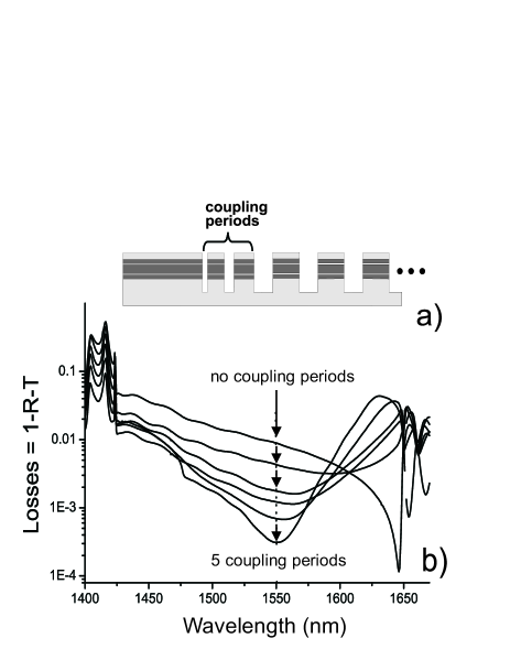
As material system we choose Si3N4 waveguides since we are investigating them as substitute of more expensive silicon on insulator waveguide JLTDaldosso . A monomode Si3N4 waveguide formed by a multilayer core of Si3N4 and SiO2 and a top-bottom cladding of SiO2, will be considered hereafter (see the experimental section IV for more details). The waveguide is interfaced to a first order Bragg mirror with a period of 490 nm which is composed by air slits (width 100 nm) etched 1m down through the bottom cladding. With these parameters the DBR supports a single guided TE polarized Bloch mode – a mode below the light-line. The characterization of the waveguide-mirror interface is made by exciting the fundamental waveguide mode and calculating the reflection (transmission ) coefficient of this mode through the waveguide-DBR system. The insertion loss spectra, defined as , are calculated from 1.4 m to 1.7 m, which includes the DBR stop band region. All the simulations have been made with a commercial software photonD based on an eigenmode expansion (EME) method Sudbo . The minimization of the insertion losses is made by means of a multiparametric optimization tool.
Optimization of the insertion losses is done by inserting coupling periods at the interface between the waveguide and the DBR. The physical lengths of each air slit and waveguide segment in the coupling periods are the free parameters of the multiparametric optimization. The numerical results of the optimization are shown in Figure (1b) where the insertion loss spectra of six optimizations are reported as a function of wavelength. The six curves correspond to different numbers of coupling periods, varied from zero (no coupling periods) to five. With increasing the number of coupling segments a well defined minimum appears at 1.55 m; the insertion losses are decreased by two order of magnitude, from for the bare mirror to for the five periods engineered mirror. Table 1 reports the parameters of the coupling periods for the five mirrors. For each engineered mirror we report the period length and the filling fraction f.f. (the ratio between the length of air slit and the period) of each set of coupling periods.
![[Uncaptioned image]](/html/cond-mat/0509779/assets/x2.png)
Table1: period length and filling fraction f.f. of each set of coupling segments for the five engineered mirror. For the periodic mirror nm and f.f.=0.204.
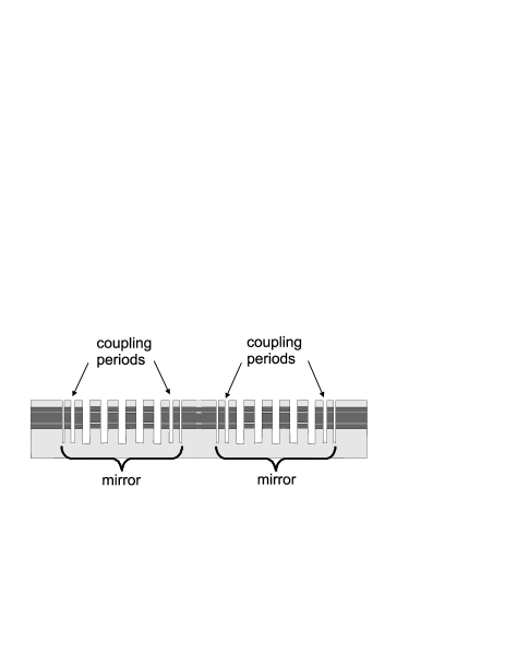
The engineered mirrors have been then used to form optimized micro-cavities (Figure 2). Figure 3 reports their calculated -factor as a function of the resonance order when no (circles), one (triangles) and two (squares) coupling periods are used. The micro-cavity intrinsic -factor was calculated from the asymptotic value of the full width at half maximum of the resonant peak as the number of DBR periods increases while the number of coupling periods is kept constant; knowing the micro-cavity resonance wavelength 1.55m, . The resonance order is defined as in Eq. 3. For the smallest defect length the minimum value of is about , due the large penetration depth of the mode defect in the mirror (see also the discussion after Eq. 3).
It is seen that the -factor increases as the number of coupling periods increases, which was expected, since the insertion losses of the mirrors decrease as shown in Figure (1). For instance at we have for no, one and two coupling periods, respectively. On the other hand, it is clearly seen that such an increase is not very regular as changes. Such a behavior is discussed in the next section.
III Interpretation of the simulation results
Let us consider a FP cavity, with mirrors characterized by complex reflectivity and transmissivity coefficients, and , respectively; the spacer between the two mirrors is characterized by a physical length and by an effective refractive index . The expression of the cavity transmission is given by the Airy formula
| (1) |
where the phase accumulated by the electromagnetic wave after half round-trip in the cavity is
| (2) |
Under the assumption that , the quality factor of the micro-cavity can be expressed as
| (3) |
where is the resonant wavelength, is the group index of cavity mode. In the eq. (3) we have also identified the resonance order with the term in square brackets divided by . The second term in brackets is proportional to the penetration depth in the mirror.

It is possible to apply this formula to our system, when the effective refractive index is taken equal to the calculated effective refractive index of the fundamental mode of the micro-cavity. The dashed lines in Figure (3) are the -factors predicted by eq. (3) for the micro-cavities with no, one and two coupling periods in the DBRs, respectively. Only the order of magnitude is got by this model, while the oscillations in the -factors found in the simulations are not reproduced. It is thus needed to go beyond this simple model and use more accurate models which predict a non linear dependence of the -factor on the mode order. In particular the theory in Ref. LalanneOptExp considers that not only the fundamental Bloch mode of the micro-cavity is excited by the fundamental waveguide mode but also radiative cavity modes. What it is worth of mentioning is that these radiative cavity modes can be coupled back into the transmitted waveguide mode, a phenomenon which can be described as a recycling of photons in the waveguide by the micro-cavity. Hence, not only the fundamental cavity mode contributes to determine the -factor of the micro-cavity but also the radiative ones. The constructive (destructive) interference among the cavity modes, which eventually increases (decreases) the -factor, depends on the cavity parameters (physical length, modal reflectivity). To simplify the calculations, the radiative cavity modes are described by a single leaky cavity mode with two complex parameters, a complex coefficient for the coupling of the cavity leaky mode with the fundamental mode and a complex effective index of the leaky mode itself. Thus, the whole process can be described by an effective reflectivity coefficient for the waveguide fundamental mode, which depends on the resonance order . The -factor is then given by a FP-like expression with the dressed reflectivity coefficient LalanneOptExp
| (4) |
The continuous lines in Figure (3) show the predictions of this model when the coupling and effective refractive coefficients are fit to the simulation data. The agreement in this case is pretty good, suggesting that the recycling of the leaky mode could play an important role in determining the performance of such micro-cavities. Even if the fit parameters have no strict physical meaning, we have checked that they take values that are compatible with leaky mode representation: the effective index of leaky mode is lower than that of the cladding, the real part of the coupling coefficient satisfies the energy conservation.
IV Preliminary experimental results
To validate the positive role of the coupling periods to increase the micro-cavity -factors, we present some preliminary experimental results for a system realized by FIB technique, starting from Si3N4 single mode waveguide. As a side-result we show that FIB technique can be effectively used to form 1D photonic crystals with good optical quality without the need to go through the lithography and etching steps used in other processing.
Slab multilayer waveguides were fabricated by low-pressure chemical vapor deposition (LPCVD) on a 2.5 m thick SiO2 and it consists of the following sequence of Si3N4 and SiO2: 100nm Si3N4, 50nm SiO2, 200nm Si3N4, 50nm SiO2 and 100nm Si3N4 Melchiorri_APL . This results in a total core layer thickness of about 500 nm. The core was capped with a 500-nm-thick cladding SiO2 layer. Lithography and etching defined channel waveguide geometries, whose nominal widths ranged from 1 to 10 m. The 1D-PhC structures were defined on the channel by using a 30 KeV Ga+ Focused Ion Beam (FIB)FIB ; Cabrini . In our experiment, we used the LEO-ZEISS 1540XB CrossBeam®, comprising a high resolution FIB column to mill directly in combination with a high precision scanning electron microscope (SEM) for precise positioning and inspection of the fabricated nanostructures in real time. Using an ion current of about 100 pA and controlling the FIB by a pattern generator (RAITH ELPHY), the pattern is directly written on the sample surface; using a total ion dose of 400 mA/cm2, a depth of about 1.3 for each structure was obtained. Figure (4) a shows a top view scanning electron microscopy (SEM) image of a Fabry-Perot samples with one coupling period.

The optical properties of integrated optical microcavities have been characterized by coupling in light from a tunable laser (1300-1630nm, 2mW) through a single mode polarization maintaining tapered fiber, mounted on a nano-positioning system. Two linear polarizers and a half-wave plate are used to control the polarization of the input signal. The collection system was provided by a near field microscope objective matched to a variable zoom mounted on a high-performance InGaAs infrared camera controlled by the LBA-500 Spiricon beam analyzer software. A prism beam splitter allows to direct the transmitted signal to a calibrated photodiode (Ge detector) to perform intensity measurements. Normalization of the transmission intensity is done with respect to a nearby reference waveguide without the 1D photonic crystals.
Figure (4b) shows the relative transmittance of transverse electric (TE) polarized light for the engineered FP microcavity of Figure (4a). The measured spectrum shows a well defined band-edge at 1380 nm and the resonant peak at 1515 nm. The first FP oscillation (corresponding to the interference of Bloch-modes of the 1D system) can be observed between 1300 and 1380 nm. The measured full width at half maximum (FWHM) of the resonance peak is 15nm which corresponds to a quality factor .
The spectrum is compared to the numerical calculation (line in Fig. 4b) and a reasonable good agreement is found for the spectral position of the FP stop-band, the resonance position and width, while the baseline in the photonic band-gap region is not reproduced due to diffraction losses and light leakages not taken into account in the calculations. The parameters (length of air slits and waveguide segments) used to reproduce the spectrum are slightly different from the nominal one by about 5%-10%. The -factor calculated with classical FP model is larger by a factor two than the measured one. This can be a good indication that anti-recycling of the leaky modes into the fundamental mode occurs in this sample. Clearly, other effects can affect the measured low values which are mostly related to the quality of the 1D photonic structures, however photon recycling effects are surely playing a role and only a more systematic study of these engineered structures could weigh the relative importance of the photon recycling effect. Such a study is under way.
V Conclusions
In this work we have presented preliminary testing of the effect of photon recycling which occurs in a 1D photonic crystals when guided and radiative modes interfere. Simulations and first measurements show that this effect could not be underestimated in optimizing the -factors of micro-cavities based on 1D photonic crystals.
We acknowledge the financial support by MIUR through FIRB (RBNE01P4JF and RBNE012N3X) and COFIN (2004023725) projects and by PAT through PROFILL project.
References
- (1) L. Pavesi and D. Lockwood (editors), Silicon Photonics, Topics in Applied Physics vol. 94 (Springer-Verlag, Berlin, 2004).
- (2) K.J. Vahala, Nature 424, 839-846 (2003).
- (3) B.S. Song, S. Noda, T. Asano and Y. Akahane, Nature Materials 4, 207 (2005).
- (4) Steven G. Johnson, S. Fan, A. Mekis, and J.D. Joannopoulos, Appl. Phys. Lett. 78, 3388 (2001).
- (5) P. Lalanne and J.P. Hugonin, IEEE J. Quant. Electr.39, 1430 (2003).
- (6) C. Sauvan, P. Lalanne, J.P. Hugonin, Nature 429, 6988 (2004).
- (7) Ph. Lalanne, M. Mias and J.P. Hugonin, Opt. Exp. 12, 458 (2004).
- (8) F. Riboli, N. Daldosso, G. Pucker, A. Lui and L. Pavesi, IEEE-Journal of Quantum Electronics 41, 1197 (2005).
- (9) N. Daldosso, M. Melchiorri, F. Riboli, M. Girardini, G. Pucker, M. Crivellari, P. Bellutti, A. Lui, L. Pavesi, IEEE Journal of Lightwave Technology 22, 1734 (2004).
- (10) Photon Design Sofware: FimmWave and FimmProp.
- (11) A.S. Sudbo, IEEE Phot. Technol. Lett. 5, 342 (1993).
- (12) M. Melchiorri, N. Daldosso, F. Sbrana, L. Pavesi, G. Pucker, C. Kompocholis, P. Bellutti, and A. Lui, Appl. Phys. Lett. 86, 121111 (2005).
- (13) K.A. Valiev, The Physics of Sub-micron Lithography (Plenum Press, 1992).
- (14) S. Cabrini, A. Carpentiero, R. Kumar, L. Businaro, P. Candeloro, M. Prasciolu, A. Gosparini, L.C. Andreani, M. De Vittorio, T. Stomeo, and E. Di Fabrizio, Microel. Eng. 78-79, 11 (2005).