Concept of deterministic single ion doping with sub-nm spatial resolution
Abstract
We propose a method for deterministic implantation of single atoms
into solids which relies on a linear ion trap as an ion source.
Our approach allows a deterministic control of the number of
implanted atoms and a spatial resolution of less than 1 nm.
Furthermore, the method is expected to work for almost all
chemical elements. The deterministic implantation of single
phosphor or nitrogen atoms is interesting for the fabrication of
scalable solid state quantum computers, in particular for silicon
and diamond based schemes. A wide range of further applications is
expected for the fabrication of nano and sub-nano electronic
devices.
PACS 03.67.-a; 29.25.Ni; 61.72.Ji; 81.16.Rf; 85.40.Ry
1 Introduction
A future solid state quantum computer (QC) may be based on implanted single ions, each of them carrying a single unity of quantum information (qubit). Logic gate operations rely on the well controlled coherent interaction between individual qubits. Any coupling to the solid state bulk material would destroy the -in general- entangled global quantum state of the device. This reasoning has led to the concept of qubits logic states which are encoded into hyperfine states of single atomic phosphorous ions 31P, embedded in a pure Si mono crystal Kane . More recently, experiments with single nitrogen-vacancy (NV) centers in diamond crystals have demonstrated single qubit operations Jel04a and two-qubit quantum logic gate operations mediated by hyperfine coupling Jel04b , and a long coherence time Kennedy as necessary for a QC according to the DiVincenco criteria roadmap .
However, the positioning accuracy of NV-defects was so far limited to 50 nm using a damage-implantation technique Martin ; Martin01 . The future quest is to fabricate an array of NV-centers with nm-precision for a scalable solid state QC. So far, no scheme for deterministic singly-charged single ion implantation has been yet reported for this spatial resolution.
The paper is organized as follows: After a short discussion of current approaches of ion implantation, we describe the novel method for single ion implantation with sub-nm spatial resolution. This includes a Paul trap as an ion source and a micro Einzel lens as an ion optical element for focusing through a pierced atomic force microscope (AFM) tip. Finally, we sketch the basic concepts of a solid state QC based upon NV color centers. Though this implantation method may be applied for a large variety of atomic species we will focus here on the specific case of N+ ions being implanted into diamond for the deterministic generation of NV color centers.
2 Ion implantation
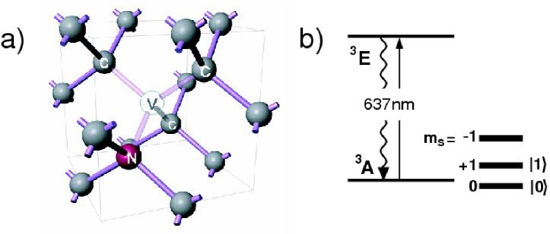
The nitrogen-vacancy center in diamond is an atomic point-defect with a structure that consists of a nitrogen atom and a vacancy in the next lattice position (Fig. 1a). It was demonstrated that NV defects can be created in nitrogen-rich (type Ib) diamond by the creation of vacancies and a subsequent annealing step Martin . During this annealing process, vacancies migrate towards nitrogen atoms forming NV defects. The major drawback of this approach is its poor positioning accuracy of defects due to the diffusion of vacancies (50 nm). Alternatively, NV defects can be created using nitrogen implantation into nitrogen-free diamond (type IIa) Kalish ; Meijer . Ion beam implantation has the advantage that the preselected position of the N-atom now defines the place of the NV center. Only the vacancies migrate during annealing (TC) as they become mobile above 650∘C. The diffusion of substitutional nitrogen starts only above 1500∘C. The creation of a single NV center relies on the migration of a vacancy to the nitrogen atom during the annealing process. The efficiency depends on the energy of the implanted ion and increases with higher energy as an increasing amount of vacancies is generated by the implantation process itself.
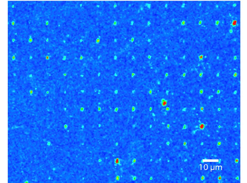
As an illustration of the latter method we show an array of NV centers generated using focused N+ ions (2 MeV) implanted into type IIa diamond (see Fig. 2). The efficiency of NV center creation at this energy is about 50% Meijer . The spot size is about 300 nm on the target surface. Due to the stochastic nature of the ion beam some spots contain more than one NV center, while others contain none. Additionally, because of the high kinetic energies of the ions the observed spot size is mostly limited by ion straggling in the diamond matrix.
However, for single ion implantation with an aspired resolution of less than 2 nm it is necessary to reduce the ion energy down to 1 keV in order to avoid lateral displacement caused by straggling111SRIM-2003: http://www.srim.org/. Recent results indicate that at these low implantation energies the efficiency of the creation of a NV defect during the annealing process is decreased to less than 10%Rabeau . Subsequent implantation of carbon ions could be used to increase the local density of vacancies near the nitrogen atom. Also other elements could be used which immediately generate color centers without the need of an additional vacancy like boron in diamond or chromium in sapphire. Regardless of the used ion species, the alignment of the ion beam is realized by a pierced AFM-tip acting as a stencil nano mask. The use of a pierced AFM-tip as a collimator is already successfully established schenkel ; patent . However, this technique has two disadvantages: First, a pinhole size of 5 nm and below will produce proximity effects, affecting the spatial resolution. Secondly, this technique needs highly charged ions for the detection of the impact of one single ion. But highly charged ions may cause severe damage to the surface schenkel98 , possibly destroying the solid state QC coherence.
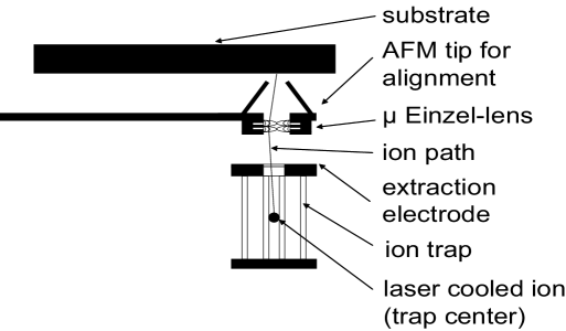
A more suitable method presented in this paper is the use of an ion trap as a single ion point source. This technique avoids any proximity effects and does not require any additional detection system. A pierced AFM tip acts as alignment tool for the ion lens with respect to the target.
The basic ideas of the proposed system are shown in Figure 3: A linear Paul trap is used as a source of single ions with supreme performance from an ion-optical point of view. Single ions are trapped, cooled and extracted with a spatial- and momentum-uncertainty near to the fundamental limit solely given by quantum physics. Additionally, the resonance fluorescence of those ions can be routinely excited by laser radiation and observed with a camera system. Thus, the number of trapped ions is well known and a deterministic implantation of a given number of atoms is possible. The ions are extracted and focused down to the surface of the substrate with sub-nm resolution using a micro Einzel lens. Advantageously, it is combined with a pierced AFM tip for the exact placement and accurate positioning of the system. In order to realize this design the following questions have to be addressed:
-
•
Is it possible to extract one ion from a Paul trap without losing the position information?
-
•
What kind of ion optics is adequate to focus ions down to nm resolution?
-
•
How to manage the adjustment procedure for single ion implantation?
-
•
What is the expected final spatial resolution of the entire system?
3 A linear Paul trap as a deterministic single ion source
Paul traps are widely used for single ion experiments Diddams01 ; teleIBK ; teleBoulder . In the specific case of a linear Paul trap, the radio-frequency (RF) voltage is applied to a set of radial electrodes and generates a pseudo potential of several eV depth. The axial confinement is provided by additional DC electrodes. Various forms and sizes of linear Paul traps are known: Typically, the RF-electrodes are in the shape of four rods Naegerl00 or four blades Schmidt03 . The applied voltages result in a harmonic trapping potential for all spatial directions. Trap sizes range from a few mm to a few 100 m in case of small linear traps Leib . Correspondingly, the vibrational trap frequencies vary from several MHz down to 100 kHz. Due to laser Doppler cooling, the kinetic energy of the trapped ions can be reduced down to a few mK (corresponding to 10-7 eV). The typical wave packet extension is 20 nm for a 14N+ ion in the ground state at a trap frequency of MHz. Routinely, the ground state of vibration is reached by more sophisticated laser cooling techniques such as resolved side band cooling on quadrupole transitions Roos99 or ground state cooling exploiting electromagnetically induced transparency (EIT) Roos00 . As a result, the position-momentum uncertainty of the ion wave function is limited only by the Heisenberg uncertainty principle.
However, ion species which might be interesting for doping applications can usually not be laser cooled. This is due to the fact that the corresponding transition wavelengths are extremely hard to achieve by laser sources or the level scheme does not feature an adequate two-level system suitable for an optical cycling transition. Unfortunately, this is the case for 31P+ and for any isotope of nitrogen. This difficulty may be circumvented by sympathetic laser cooling Drewsen04 ; Drewsen01 ; Rohde01 ; Barett03 . We propose to sympathetically cool either phosphorous or nitrogen doping ions inside a string of 40Ca+ ions which are laser cooled. The linear crystal of 40Ca+ ions will be observed with a CCD-camera whereas the doping ions show up as dark sites NaegerlDiss ; Drewsen01 (Fig. 4). After Doppler cooling, a second cooling step via EIT will allow to reach almost the vibrational ground state of all common modes of vibration Schmidt01 .
Then, a single dark doping ion is separated together with a single 40Ca+ ion from the entire crystal in order to determine the mass of the doping ion by measuring the vibrational frequency of the mixed crystal Drewsen04 . The observation of dark sites in the fluorescence, the ground state cooling, and the deterministic separation of the doping ion are the key-elements of our method.
Finally, the ion is extracted for implantation, being delivered with an ideal brightness at the physical limit.
4 Point source ion optics
The ion trap for single ions defines a completely new starting point for ion beam optics offering an ideal point source perfectly suitable for deterministic ion ray tracing. The theoretical accuracy limit of the point source is given by the uncertainty of the initial velocity distribution after optical cooling. Beam broadening by stochastic space charge effects is completely avoided.
For the numerical simulation of the ion’s trajectory we first model the quasi-electrostatic potential of the Paul trap and then simulate the trajectories by ray tracing. In order to cross-check the results, two fully independent software packages have been developed.
Method A relies on the calculation of the potential distribution of the trap and extractor lens using a finite-differential method (FDM) combined with a multi-grid technique to find starting values for a simultaneous over-relaxation (SOR) method nr . The calculation of the trap potential is performed on a 64x64x256 grid. The grid distance is chosen to be 100 m. A ray tracing procedure uses the resulting field distribution to calculate the electric force acting on the ion using a 5th order Runge-Kutta formalism with adaptive step size control nr . A Monte-Carlo technique simulates the influence of starting parameters. The temperature is set as starting parameter for the random choice of the initial ion velocity. Method B applies the commercial program Femlab222Femlab: http://www.comsol.com/ for calculating the 3D trap potentials in an adaptive non-uniform grid. The trajectories are simulated in C++ in a 8th order Runge-Kutta Prince-Dormand method333GSL: http://www.gnu.org/software/gsl/.
In both simulations, the type and size of the linear quadruple ion trap is adapted from NaegerlDiss ; Naegerl00 . The trap consists of four parallel rods with 2 mm spacing and a length of 10 mm. Diagonally opposed rods are connected to a RF source with of 18 MHz and kV, generating a quadrupole RF field. The axial confinement is provided by two disc shaped end caps at a distance of 10 mm (outer diameter 6 mm) with a centered extraction hole of 1 mm diameter. The DC voltage at the end caps is set to 500 V. The parameters for the end caps are slightly modified to Naegerl00 .
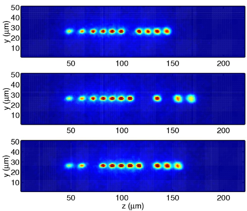
To use the trap as an ion source all potentials are biased by +500 V and the temperature of the ions is assumed to be around 0.1 mK. The extraction of the ion is initiated by switching one of the end caps from 1000 V to 0 V. Both simulation methods show that sub-nm resolution (1 nm) can be achieved with laser cooled ions. In the following we will focus only on the results of method B. The rays of the ions inside the trap after extraction are shown in Figure 5. One of the important questions for the optimization is the handling of the RF-field during the extraction procedure. Our first guess was to continuously apply the RF-field during extraction in order to maintain the radial confinement (Fig. 5, dashed). The lateral spread of the ion trajectories at a distance of 10 mm from the trap center in the extraction direction is about 50 nm. In order to focus the trajectories down to one spot at the target we simulate a small electrostatic Einzel lens between trap and target, located at a distance of 90 mm from the trap center. The symmetric Einzel lens consists of a stack of three equidistant conducting layers separated by about 150 m. The middle layer is biased to +1000 V whereas the other layers are grounded. The resulting focal length for 500 eV ions is about 300 m (Fig. 6, dashed). The spread of the impact positions of the ions at the target plane (Fig. 7b) is about 20 nm which would be still one order of magnitude too high. If the position of the target plane is changed within 1 m the spot size hardly changes (Fig. 7a-c). This situation cannot be improved by further lowering the initial temperature of the ions in the trap. The spread is caused by axial velocity kicks caused by the RF field near the extraction electrode, which lead to different focal lengths of the Einzel lens (chromatic abberation). Therefore in a future setup the ion lens will be designed to minimize chromatic abberation. If in our simulation the RF field is switched off before the ion has reached the end caps, e.g. 6 periods after start of the extraction, we observe a slightly larger spatial spread of the ions after the trap (Fig. 5, solid) and before the ion lens (Fig. 6, solid) but the velocity spread in axial direction is strongly reduced from to resulting in a spot size of around 1 nm at the target plane (Fig. 7e). In order to guarantee the latter velocity spread the power supplies have to be stabilized to a level of about 0.5mV.444This is quite challenging especially as the voltage has to be switched. If the position of the target plane is now changed within 1 m the spot size changes drastically (Fig. 7d-f). Beside this focussing effect, the lens has an additional advantage: The ions move always towards the lens axis. A small displacement and misalignment of the ion trap will not affect the impact position at the target and makes the system insensitive against expected mechanical vibrations and thermal drifts.


The simulated variation of lateral positions of the ion at the target’s location as a function of the ion temperature is shown in Fig. 8. A displacement below 1 nm can be expected for an ion with a temperature below 0.2 mK if spherical abberation at the ion lens can be avoided. This is routinely achieved with laser cooling techniques. The simulations also show that a preadjustment between the trap and the lens within a few m is necessary to achieve a spot size in the order of a few nm. The focal depth of the lens is about 1 m and requires a preadjustment of the lens voltage. This can be done offline using a low energy ion gun combined with a detection system, see Section 5.
For ion beam optics at very low kinetic ion energies AC stray magnetic fields as produced by electric engines or radio waves are very serious. Fortunately, the ion inside the trap is shielded due to the RF trap field. Simulations show that AC stray magnetic fields have to be reduced below 0.5 T in order to reach nm resolution.
5 AFM set-up with integrated hollow tip
With a focal depth of the Einzel lens of about 1 m the distance to the target needs accurate preadjustment. Additionally, lateral positioning of the doping sites with respect to surface structures, e.g. markers or electric gate assemblies is required. The alignment accuracy of a few nm is desirable for functional device realization. The only known systems that allow addressing with sub-nm resolution are atomic-force microscopes (AFM) or scanning-tunneling microscopes (STM).
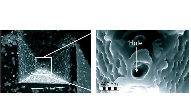
We take advantage of a recent breakthrough in AFM technology: The cantilever probe consists of a SiN-tip with a hollow nitride pyramid with a drilled hole (30 nm diameter) fabricated by focused ion beam (FIB) milling (Fig. 9) Rang96 . For this process the Rossendorf IMSA-Orsay Physics FIB was applied at an energy of 25 keV and a spot size of about 25 nm. A faraday cup under the tip was installed as an end point detector to stop the milling just in time as well as to image the hole by the transmission current signal. The diameter of the entrance of the milled hole was about 140 nm and the exit was in the range of 30 nm. The AFM operation with piezo resistive cantilevers Rang02 ; Rang05 allows imaging of the surfaces’ topography in conventional contact mode with a resolution in z better than 1 nm and also in non-contact mode employing integrated thermal bimorph actuators Ped03 . The Einzel lens is combined with the AFM cantilever mount (Fig. 3) to achieve a high correlation and stability between AFM tip and focus position of the lens. In contrast to Kennedy the AFM tip has no direct ion optical function any more and will not be hit by the beam. To avoid any kind of contamination during the loading of the ion trap, an aperture size in the range of 30-50 nm is useful.
6 Application of single ion implantation for quantum computing
For the realization of a solid state quantum computer several technical issues have to be solved. The major requirement is the existence of well defined qubits which can be reliably fabricated and controlled. Especially for solid-state systems, proper choice of the qubit is a challenging task because of decoherence caused by strong interactions within the bulk material. The most important issue at the moment is to proof the scalability of those qubit systems. There are several possible approaches like qubits based on quantum dots, superconducting nanostructures and nuclear spins in semiconductors Kane ; Li ; Yama . The latter were envisaged as promising candidates because of very long coherence times (up to seconds) Ladd . However, the readout with conventional NMR technology gives only access to ensemble spin states and thus causes severe scalability problems Warren97 . Recently, it was shown, that the single electron spin of a NV center in diamond can be read out optically. As sketched in Figure 1b, the electronic level scheme exhibits a strong dipole-allowed optical transition with a zero-phonon line at 1.945 eV. A second essential feature of the NV-defect is a paramagnetic ground electronic state which originates from two unpaired electron spins Oort ; Reddy ; Redman . The dipolar interaction between these electronic spins leads to a zero-field splitting between and ground state spin sublevels. The readout of the electron spin is based on the fact that under excitation of the optical dipole transition (Fig. 1b) the amount of scattered photons is sensitive to the internal spin state Jel04c .
A two qubit quantum gate was demonstrated using the hyperfine coupling between nuclear and electron spins associated with a single defect Jel04b . Scaling up to a multitude of defects is impeded because of the local nature of the hyperfine interaction Wracht . Hence long range dipolar coupling between spins is more appropriate for scalable QC. Note that only neighboring qubits will be coupled substantially due to the dependence of the coupling. Single qubits may be encoded in electron spin states of single NV defects and fast quantum gate operations will be performed using electron spin dipole-dipole coupling between closely spaced defects.555Alternatively, the dipole-dipole interaction between electronic (optical) transitions could also be explored for coupling between qubits. Thus, the coupling strength would be controlled via a selective optical excitation of the defect centers. As opposed to the hyperfine coupling, now, distances of 1 nm are sufficient for achieving a resolvable coupling of 50 MHz. Such interqubit spacings are technically feasible by the above described method. CNOT and other quantum gate operations between adjacent electron spins may be implemented using ESR analogues of well developed NMR pulse sequences Twamley ; Vandersypen . As an example, refocusing techniques using broad pulses resonant to all spins may be used for switching off all interactions between any spins. In order to selectively enable the interaction between specific adjacent spins an additional spectrally narrow pulse sequence has to be inserted between the refocusing pulses. The coherence time of spins associated with defects in diamond is amazingly long with a few tens of microseconds at room temperature Kennedy .666Decoherence due to coupling to imperfections on the surface is not expected, since the surface of diamond can be prepared by a well controlled way using acid or H-plasma treatment. The two qubit gate operation timescale is limited by the coupling strength in the range of tens of MHz. This will allow to reach the quantum error correction threshold of .
7 Conclusions
We have presented a novel method for deterministically implanting single ions with sub-nm resolution. Key elements of our method are a linear Paul trap serving as an ion source in combination with sophisticated laser cooling techniques such as EIT cooling to the vibrational ground state. This atom optical element constitutes an ideal deterministic point source of ions with the ultimate brightness only limited by the Heisenberg uncertainty principle. Our simulations predict a lateral positioning accuracy of the ions of less than 1 nm for an ion-temperature of 0.2 mK reached by laser cooling techniques.
In the future we will optimize the design of the ion trap. The ion optical system has to be designed in such a way that chromatic abberation is minimized. Experiments will be performed with various doping ions in order to explore a broad spectrum of applications. The application of our technique can also be extended to molecular or cluster particles.
8 Acknowledgement
We acknowledge financial support in Bochum by the Volkswagen foundation. The work in Stuttgart has been supported by the DFG via SFB/TR 21. Financial support in Stuttgart and Ulm is granted by the Landestiftung BW via the program “Atomoptik”.
References
- (1) B. E. Kane, Nature 393, 133 (1998)
- (2) F. Jelezko, T. Gaebel, I. Popa, A. Gruber, and J.Wrachtrup, Phys. Rev. Lett. 92, 076401 (2004)
- (3) F. Jelezko, T. Gaebel, I. Popa, M. Domhan, A. Gruber, and J. Wrachtrup, Phys. Rev. Lett. 93, 130501 (2004)
- (4) T. A. Kennedy, J. S. Colton, J. E. Butler, R. C. Linares, and P. J. Doering, Appl. Phys. Lett. 83, 4190 (2003)
- (5) A Quantum Information Science and Technology Roadmapping Project by the Advanced Research and Development Activity (ARDA), http://qist.lanl.gov/ and European Pilot project http://qist.ect.it/
- (6) J. Martin, R. Wannemacher, J. Teichert, L. Bischoff, and B. Köhler, Appl. Phys. Lett. 75, 3096 (1999)
- (7) J. Martin, L. Bischoff, and R. Wannemacher, Opt. Comm. 188, 119 (2001)
- (8) R. Kalish, C. UzanSaguy, B. Philosoph, V. Richter, J. P. Lagrange, E. Gheeraert, A. Deneuville, and A. T. Collins, Diamond and Related Materials 6, 516 (1997)
- (9) J. Meijer, B. Burchard, M. Domhan, C. Wittmann, T. Gaebel, I. Popa, F. Jelezko, and J. Wrachtrup, Appl. Phys. Lett. 87, 261909 (2005)
- (10) J. R. Rabeau, P. Reichert, G. Tamanyan, D. N. Jamieson, S. Prawer, F. Jelezko, T. Gaebel, I. Popa, M. Domhan, and J. Wrachtrup, Appl. Phys. Lett. 88, 023113 (2006)
- (11) T. Schenkel, A. Persaud, Journal of Applied Physics 94, 7017 (2003)
- (12) I. Rangelow, J. Meijer, and T. Schenkel, German Patent Appl., DE10347969A1,2003 (patent pending)
- (13) T. Schenkel, A. V. Hamza, A. V. Barnes, D. H. Schneider, J. C. Banks, and B. L. Doyle, Phys. Rev. Lett., 81, (1998)bf81, 2590 (1998)
- (14) S. A. Diddams, Th. Udem, K. R. Volgel, C. W. Oates, E. A. Curtis, W. D. Lee, W. M. Itano, R. E. Drullinger, J. C. Bergquist, and L. Hollberg, Science 293, 825 (2001)
- (15) M. Riebe, H. Häffner, C. F. Roos, W. Hänsel, J. Benhelm, G. P. T. Lancaster, T. W. K rber, C. Becher, F. Schmidt-Kaler, D. F. V. James, R. Blatt, Nature 429, 734 (2004)
- (16) M. D. Barrett, J. Chiaverini, T. Schaetz, J. Britton, W.M. Itano, J.D. Jost, E. Knill, C. Langer, D. Leibfried, R. Ozeri, and D.J. Wineland, Nature 429, 737 (2004)
- (17) H. C. Nägerl, Ch. Roos, D. Leibfried, H. Rohde, G. Thalhammer, J. Eschner, F. Schmidt-Kaler, and R. Blatt, Phys. Rev. A 61, 023405 (2000)
- (18) F. Schmidt-Kaler, H. Häffner, S. Gulde, M. Riebe, G. P. T. Lancaster, T. Deuschle, C. Becher, W. Hänsel, J. Eschner, C. F. Roos, R. Blatt, Appl. Phys. B: Lasers and Optics 77, 789 (2003)
- (19) D. Leibfried, T. Schätz, Physik Journal 3 23 (2004)
- (20) C. F. Roos, Th. Zeiger, H. Rohde, H.C. N gerl, J. Eschner, D. Leibfried, F. Schmidt-Kaler, R. Blatt, Phys. Rev. Lett. 83, 4713 (1999)
- (21) C. F. Roos, D. Leibfried, A. Mundt, F. Schmidt-Kaler, J. Eschner, R. Blatt, Phys. Rev. Lett. 85, 5547 (2000)
- (22) M. Drewsen, A. Mortensen, R. Martinussen, P. Staanum, J. L. Sørensen, Phys. Rev. Lett. 93, 243201 (2004)
- (23) L. Hornekær, N. Kjærgaard, A. M. Thommesen and M. Drewsen, Phys. Rev. Lett. 86, 1994 (2001)
- (24) H. Rohde, S. T. Gulde, C. F. Roos, P. A. Barton, D. Leibfried, J. Eschner, F. Schmidt-Kaler, R. Blatt, J. Opt. B3, 34 (2001)
- (25) M. Barrett, B. L. DeMarco, T. Schätz, V. Meyer, D. Leibfried, J. Britton, J. Chiaverini, W. M. Itano, B. M. Jelenkovic, J. D. Jost, C. Langer, T. Rosenband, and D. J. Wineland, Phys. Rev. A 68, 042302 (2003)
- (26) H. C. Nägerl, Ion Strings for Quantum Computing, Dissertation, Innsbruck (1998), unpublished.
- (27) F. Schmidt-Kaler, J. Eschner, G. Morigi, C. F. Roos, D. Leibfried, A. Mundt, R. Blatt, Appl. Phys. B73, 807 (2001)
- (28) W. H. Press, S. A. Teukolsky, W. T. Vetterling, B. P. Flannery, Numerical Recipies in C, (Cambridge Univeristy Press Cambridge 1992).
- (29) I. W. Rangelow, F. Shi, P. Hudek, T. Gotszalk, P. B. Grabiec, P. Dumania, SPIE Vol. 2879, 56 (1996)
- (30) I. W. Rangelow, P. Grabiec, T. Gotszalk, and K. Edinger, Piezoresistive SXM sensors, Surface and Interface Analysis, Vol. 33, (2002) pp. 59-64
- (31) I. W. Rangelow, Piezoresistive Scanning Proximity Probes for Nanoscience, Technisches Messen 72, (2005) pp. 103-110
- (32) R. Pedrak, Tzv. Ivanov, K. Ivanova, T. Gotszalk, N. Abedinov, and I. W. Rangelow, K. Edinger, E. Tomerov, T. Schenkel, and P. Hudek, J. Vac. Sci. Technol. B 21, 3102 (2003)
- (33) X. Q. Li, Y. W. Wu, D. Steel, D. Gammon, T. H. Stievater, D. S. Katzer, D. Park, C. Piermarocchi, and L. J. Sham, Science 301, 809 (2003)
- (34) T. Yamamoto, Y. A. Pashkin, O. Astafiev, Y. Nakamura, and J. S. Tsai, Nature 425, 941 (2003)
- (35) T. D. Ladd, J. R. Goldman, F. Yamaguchi, Y. Yamamoto, E. Abe, and K. M. Itoh, Phys. Rev. Lett. 89, 017901 (2002)
- (36) W. S. Warren, Science 277, 1688 (1997)
- (37) E. van Oort, P. Stroomer, and M. Glasbeek, Phys. Rev. B 42, 8605 (1990)
- (38) N. R. S. Reddy , N. B. Manson, and E. R. Krausz, Journal of Luminescence 38, 46 (1987)
- (39) D. Redman, S. Brown, and S. C. Rand, Journal of the Optical Society of America B9, 768 (1992)
- (40) F. Jelezko, and J. Wrachtrup, Journal of Physics: Condensed Matter 16, (2004) R1089.
- (41) J. Wrachtrup, S. Kilin, and A. P. Nizovtsev, Opt. Spectrosc. 91(3), 429 (2001)
- (42) J. Twamley, Phys. Rev. A 67, (2003) 052318.
- (43) L. M. K. Vandersypen and I. L. Chuang, Rev. Mod. Phys 76, 1037 (2004)