Raman spectroscopy and field emission measurements on catalytically grown carbon nanotubes
Abstract
We used microcontact printing to pattern a silicon surface with an iron-containing catalytic solution. Multi-wall carbon nanotubes were subsequently grown on the patterned areas by chemical vapor deposition at temperatures between 650 and 1000∘C. We demonstrate that the diameter of the catalytically grown multi-wall nanotubes increases with the deposition temperature. Raman spectroscopy has been used to investigate the crystalline character of the obtained structures and it is found that the fraction of the nano-crystalline shell increases with the temperatures. The measurement of the field emission properties shows a correlation between the tube diameter and the emission field values.
Introduction
Carbon nanotubes IIJIMA have been studied already for several years and are now considered for applications in miscellaneous devices such as tubular lamps CHATELAIN , flat panel displays KIM , lighting elements YAMAKAWA or nanometric electronic devices DEKKER ; YAMAKAWA2 . Such devices make precise demands on the properties of the tubes, as the length, diameter and electronic properties have a strong influence on the final performance of the device. This implies that the nanotube growth has to be controlled and understood. However, we still lack an exact knowledge of the growth mechanism, be it for arc discharge, laser ablation, or catalytic growth IIJIMA2 .
One of the most promising properties which should be exploited for applications is the very good field emission of the nanotubes WEISS . The catalytic deposition is the most practical method to create nanotubes on vast surfaces. In a recent paper we studied the deposition conditions of the catalytic growth of multiwalled carbon nanotubes KERN . We found that the catalyst had an influence on the morphology of the grown structures, and that Fe was better suited for the low temperature growth of nanotubes than Ni or Co. We also noted that the diameter of the nanotubes increases with the deposition temperature. We present here advanced investigations on the structures obtained with Fe as catalyst. We performed Raman and Transmission Electron Microscopy (TEM) studies to elucidate the crystalline structure of these objects. In respect of applications we also completed the research on these structures with the study of their field emission properties. We demonstrate that combing field emission measurements, Scanning Electron Microscopy (SEM), Raman spectroscopy and TEM allows an optimization of crystallinity, geometry and field emission while gaining new information about the structure of the considered objects.
Experimental methods
Synthesis of nano-structured material
Microcontact printing (CP) was performed to pattern a 100-oriented boron doped silicon wafer (resistivity: 5 - 25 mcm) KERN . The stamps for CP were obtained by curing poly(dimethyl)siloxane (PDMS) for at least 12 h at 60∘C on a structured master which was prepared by contact photolithography. The structures of these stamps are squares with a width of 5 m. They were hydrophilized before use by a oxygen plasma treatment (O2 pressure 0.8 mbar, load coil power 75 W, 60 s). The catalyst solution for the CP was a 100 mM solution of Fe(NO3)9H2O in ethanol. The catalyst concentration of 100 mM was chosen since at this amount a dense, but well-separated growth of nanotubes is obtained with good reproducibility KERN . For printing the stamp was loaded with 0.2 ml of catalyst solution for 30 s and then dried in a nitrogen stream for 10 s. The printing was performed by placing the stamp on the surface of the SiO2/Si wafer for 3 s.
The catalytic growth of nanotubes was carried out in a flow reactor (quartz tube with an inner diameter of 14 mm in a horizontal oven) directly after the printing. Before the deposition the volume of the quartz tube was rinsed by a nitrogen stream of 80 ml/min. The deposition was performed with 80 ml/min of nitrogen and 20 ml/min of acetylene (carbon source for the catalytic growth) at atmospheric pressure.
Characterization techniques
Scanning electron microscopy (SEM) was performed to analyze the microstructures in plan view. A Philips XL 30 microscope equipped with a field emission gun (FEG) was used with an acceleration voltage between 3 and 5 kV, a working distance of 10 mm, and in secondary electron (SE) image mode.
The growth morphology and crystallinity of the tubular structures were controlled by transmission electron microscopy (TEM). For this purpose a Philips EM 430 microscope equipped with a Gatan image plate operating at 300 kV (point resolution 0.3 nm) was used.
Information about the vibrational properties of the nanostructures was obtained by micro-Raman spectroscopy. The Raman spectra were recorded in backscattering configuration using the 514.5 nm line of an Ar+ ion laser and a DILOR XY 800 spectrometer. An incident maximum laser power of 20 mW was applied in order to avoid peak shifts due to thermal heating or structure transformations during data acquisition. A spot size of approximately 2 m was achieved with a 250 Olympus microscope objective. The spectra were calibrated using a natural diamond single crystal.
The field emission measurements were performed using the examined samples as cathodes. The emitted electrons were collected on a highly polished stainless steel spherical counterelectrode of 1 cm diameter, which corresponds to an emission area of 0.007 cm2. The distance between the electrodes was adjusted to 125 m. A Keithley 237 source-measure unit was used to supply the voltage (up to 1000 V) and to measure the current with pA sensitivity, allowing the characterization of current-voltage () behaviour.
Results
Morphology
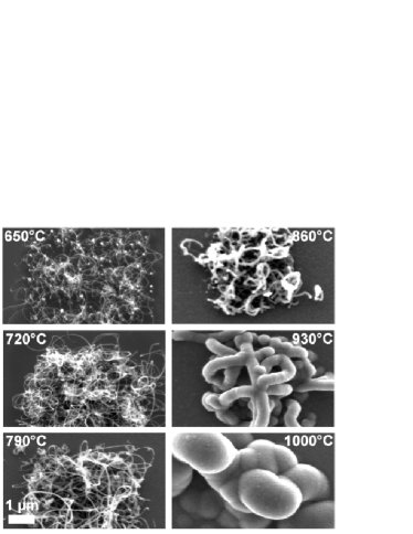
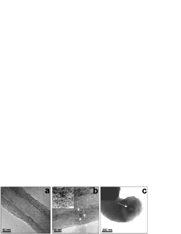
The influence of the deposition temperature on the morphology of the carbon structures is demonstrated for a deposition time of 30 min on Fig. 1. The carbon nanotubes and carbon structures grow with random orientation from iron-inked squares of a silicon surface. One can nicely see the increase of the diameter from thin nanotubes at 650∘C to thick “carbon worms” at 1000∘C. The diameter varies between 25 nm for the structures at 650∘C and about 1 m for the structures at 1000∘C. TEM reveals that multi-wall nanotubes grown at 650∘C are hollow and well-graphitized (Fig. 2a) . The well-separated nanotubes have an inner diameter of about 15 nm and an outer diameter of about 30 nm. Most of them have open ends and some nanotubes contain encapsulated catalyst particles. In about ten percent of the nanotubes we found these particles at the top of the tube. In this case, the particles are of prolate shape and aligned in the growth direction KERN .
The carbon structures grown at higher temperatures consist of a “nanotube core” and an additional layer of amorphous or polycrystalline carbon. Fig. 2b shows a TEM image of the structures obtained at 930∘C where a core structure is surrounded by flake-like carbon (indicated by arrows in Fig. 2b). The structures at 1000∘C are too thick to be imaged by TEM due to the electron transparency.
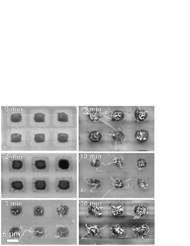
We also found that the growth of the nanotubes is a very fast process: under our conditions the growth takes place during the first 5 min already. Fig. 3 shows the evolution of the nanotube growth with time at 720∘C. After the annealing without the CVD process only the printed catalyst patterns are visible. After 2 min of deposition some dots of carbonized catalyst appear in the center of the printed squares. Only 1 min later, we detect nanotubes of up to 10 m length, which implies that the growth rate is of at least 160 nm/s. In the following time the density of the nanotubes increases but we cannot detect a significant increase in length. The maximum length remains at about 10 m.
Raman spectroscopy
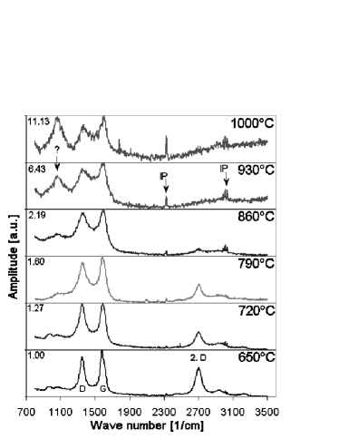
We performed micro-Raman spectroscopy in order to investigate the vibrational properties of the synthesized carbon structures, which allows also to draw further conclusions about their crystallography or morphology. Fig. 4 compares the Raman spectra measured from carbon nanotubes grown at temperatures between 650∘C and 1000∘C. All spectra show at least the two significant peaks at 1580 cm-1 and at 1347 cm-1, which become broader at higher temperatures and overlap.
Crystalline graphite leads to a sharp vibration mode at 1580 cm-1 KOENIG which is due to the presence of C-sp2 domains and named first order G band. The peak at approximately 1350 cm-1 is considered to represent a more disordered structure and is labeled as D (disordered) band KATKANANT . Note that in a perfect graphite crystal the first order vibrational mode of the D band is forbidden due to the selection rules. Decreasing particle size or bending of the lattice fringes may activate this band. As seen in Fig. 4, the second order D peak (2.D) appears at approximately 2700 cm-1 for nanotubes grown at lower temperatures. However, with increasing deposition temperature this peak disappears. The spectra are normalized to the highest peak in each spectrum (the G-peak). The signal strength gets weaker for the structures deposited at higher temperatures, therefore the noise level becomes more and more visible in the spectra.
It is known (e.g. WITHE ; ANDERSON ) that smaller particles as well as structural imperfections will broaden the first order peaks from graphite. Therefore one can estimate the order of crystallinity in the material from the corresponding halfwidth (FWHM). An amorphous structure leads typically to a halfwidth (FWHM) of approximately 200 cm-1 ANDERSON as observed in the case of deposition at 1000∘C. In the case of nanotubes deposited at 650∘C sharp peaks (FWHM 90 cm-1) reveal their much higher degree of crystalline perfection.
The catalytically grown carbon nanotubes can be characterized as a nano-crystalline but disordered graphite-like system where the disorder increases with the preparation temperature. This confirms qualitatively the results obtained by TEM. Unfortunately, Raman measurements could not clearly confirm that the high temperature carbon structures consist of an amorphous and of a crystalline part as suggested by TEM.
Interestingly, the relative height of the peak at about 1047 cm-1 increases with temperature. This peak could not yet be identified, but its broad shape indicates that it could probably originate from solid state phonons. We already detected this peak in earlier experiments on nitrogenated carbon nanotubes KARIMI . Some other peaks as indicated by arrows in Fig. 4 might be due to impurities. Stretch vibrations of N2 in the ambient air might cause the sharp peak at about 2325 cm-1 WOTTKA .
Field emission
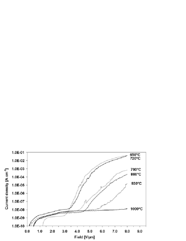
In Fig. 5 we present the results of the field emission measurements of the obtained carbon films. We noted a decrease of the absolute current density at given applied field with increasing deposition temperature. The turn-on field (field to obtain a current density of 10-5 A/cm2, first illumination of a screen pixel) and the threshold field (field at a current density of 10-2 A/cm2, saturation of a screen pixel) both increase with increasing deposition temperature (Tab. 1). For the carbon structures deposited at temperatures of 790∘C and above the current density for the threshold field of 10-2 A/cm2 was not reached below the maximal applied voltage of 1000 V at 125 m interelectrode distance.
The field amplification factor was calculated with the Fowler-Nordheim formula. The model describes the electron emission from a flat surface by tunneling through the triangular surface potential barrier. The emitted current is proportional to , where is the applied field just above the emitting surface, is the work function and is a constant (V eV3/2 m-1) PLUMMER . Generally, is not known exactly and is therefore taken here as , with the applied voltage , the interelectrode distance and the macroscopic applied field . The work function was assumed to be equal to 5 eV, which is a reasonable assumption for carbon-based field emitters SCHLAPBACH .
The field amplification values do not follow a simple trend with temperature, as can be extracted from Tab. 1. It is well-known that for a single tube, a larger diameter will lower the field amplification factor for a given length. The increase of the diameter found in Fig. 1 should thus result in a monotonously decreasing field amplification factor. Our experimental results suggest that this trend is masked (at least in part) by varying nanotube lengths and nanotube densities on the samples, which lead to more or less pronounced screening effects CHATELAIN2 . The comparison with the SEM images suggest that the field emission corresponds to the geometry of the structures and that the structures with a smaller diameter emit better. This behavior was also observed earlier for nitrogenated carbon structures KLINKE .
Discussion
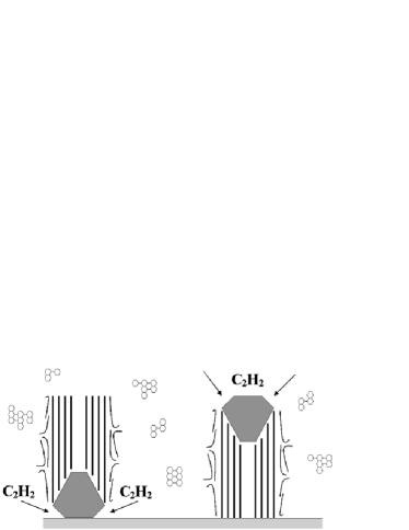
We discuss in the following our results in the light of the most probable growth mechanism for carbon nanotubes under our experimental conditions. Acetylene is stable at temperatures below 800∘C and can be only catalytically dissociated, in our case on the small metal (oxide) particles delivered to the substrate by microcontact printing (Fig. 6). The dissociation reaction takes presumably place at facets of well-defined crystallographic orientation, and the resulting hydrogen H2 is removed by the gas flow whereas the carbon is dissolved in and diffuses into the particle DING . For unsaturated hydrocarbons this process is highly exothermic. When the particle is saturated with carbon, the carbon segregates on another, less reactive surface of the particle, which is an endothermic process. The resulting density gradient of carbon dissolve in the particle supports the diffusion of carbon through the particle. To avoid dangling bonds, the carbon atoms assemble in a sp2 structure at a less reactive facet of the particle, which leads to the formation of a nanotube.
We noted in Fig. 3 that the nanotube growth did not begin immediately after the introduction of the hydrocarbon gas in the reactor, but that some carborized spots appear before the rapid nanotube growth. This suggests that a certain quantity of carbon must be dissolved into and diffuse through the particle before the nanotube growth can start.
The simple model presented in Fig. 6 describes the growth with a particle at the top of the nanotube or at the bottom. In the second case the particle sticks more to the substrate surface than in the first case. But there must be free particle surfaces which are exposed to the gas to proceed the growth. In the second case the acetylene diffuses from the side into the particle and the nanotube is constructed from the bottom up, whereas in the first case the gas diffuses from the sides and form the top into the particle. This seems to be the favored mechanism in our case as typically 90 % of the tubes have closed tips without a catalytic particle.
It is at first glance difficult to understand why the diameter of the structures increases with the temperature above 800∘C in the frame of the above model. At around 800∘C, acetylene starts to dissociate spontaneously, and the reaction gas contains therefore a significant fraction of free carbon, which will form larger aggregates in order to avoid dangling bonds. These carbon flakes, once formed, are carried with the gas flow and may be deposited on the substrate. We therefore propose the following scenario at temperatures above 800∘C: as is the case at lower temperatures, carbon nanotubes of small diameter are formed over the catalyst patterned areas after an activation period, while the growth itself takes place very rapidly. In addition, the flakes formed in the gas phase condensate on the substrate and on the formed nanotubes, adding a polycrystalline outer shell over the graphitic inner core. The structures get thicker with temperature because the proportion between dissociated and molecular acetylene in the gas phase increases.
This explanation is supported by the TEM images and the Raman spectroscopy, which confirmed the polycrystalline character of these structures. In fact, while SEM suggests an amorphous carbon structure on the surface of the grown tubes, TEM reveals a crystalline core structure which is surrounded by a polycrystalline shell (Fig. 2b and c). Raman spectroscopy showed that there is a continuous increase of the polycrystalline fraction in the structures what corroborates the findings. The outer shell becomes thicker with higher temperature starting from the thinnest structures at a temperature of 650∘C.
The results of the field emission experiments show that the thinnest nanotubes are more efficient field emitters. The field emission properties (emission fields, field amplification factor) follow loosely the morphology of the individual tubes, as the emission fields decrease with increasing temperature. It seems however that the overall structure of the nanotube film, such as nanotube density and height, plays a role that is more important than the diameter of the structures because of screening effects.
The crystallinity of the nanotubes may also influence the field emission properties. As the work function of polycrystalline and graphitic carbon are very similar, the main difference between the two forms is their electrical resistivity, which is lower in the case of well-graphitized carbon. A higher resistivity will lead to higher emission fields as a voltage drop will appear along the tube, reducing the effective applied field. However, this effect will play a role only at high current densities, and that it will have little influence on the low current part of the I-V curve. Therefore significant differences in turn-on field and field enhancement factor between well-graphitized and polycrystalline nanotubes of equivalent dimensions are not expected. The major factor that determines the field emission properties is the nanotube diameter, length and spacing.
Conclusions
We have grown carbon nanostructures by thermal CVD with an iron catalyst that was delivered to the Si substrate by microcontact printing. We noted that the diameter and morphology of the produced structures varied with the deposition temperature, from thin and well-graphitized carbon nanotubes at 650∘C to m-thick fibers at 1000∘C. We used TEM imaging, Raman spectroscopy and field emission experiments to investigate in more detail the character of these structures, and found that the increase in temperature above 800∘C resulted in the formation of a polycrystalline outer shell over a nanotube core. We suggest that this effect is due to the dissociation of acetylene in the gas phase, which leads to the formation of carbon flakes that are subsequently deposited on the catalytically grown structures.
Acknowledgement
The Swiss National Science Foundation (SNF) is acknowledged for the financial support. The electron microscopy was performed at the Centre Interdépartemental de Microscopie Electronique (CIME) of EPFL. The authors are grateful to Heiko Seehofer from Département des Materiaux of EPFL for technical assistance in Raman spectroscopy.
References
- (1) Iijima, S. Nature 1991, 354, 56.
- (2) Bonard, J. M.; Stöckli, T.; Noury, O.; Châtelain, A. Appl. Phys. Lett. 2001, 78, 2775.
- (3) Choi, W. B.; Chung, D. S.; Kang, J. H.; Kim, H. Y.; Jin, Y. W.; Han, I. T.; Lee, Y. H.; Jung, J. E.; Lee, N. S.; Park, G. S.; Kim, J. M. Appl. Phys. Lett. 1999, 75, 3129.
- (4) Murakami, H.; Hirakawa, M.; Tanaka, C.; Yamakawa, H. Appl. Phys. Lett. 2000, 76, 1778.
- (5) Yao, Z.; Postma, H. W. C.; Balents, L.; Dekker, C. Nature 1999, 402, 273.
- (6) Hirakawa, M.; Sonoda, S.; Tanaka, C.; Murakami, H.; Yamakawa, H. Appl. Surf. Sci. 2001, 169, 662.
- (7) Charlier, J. C.; Iijima, S. in: M. S. Dresselhaus, G. Dresselhaus, P. Avouris (Eds.), Carbon Nanotubes (Springer, 2001).
- (8) Bonard, J. M.; Croci, M.; Klinke, C.; Kurt, R.; Noury, O.; Weiss, N. Carbon 2002 in press.
- (9) Klinke, C.; Bonard, J. M.; Kern, K. Surf. Sci. 2001, 492, 195.
- (10) Tuinstra, F.; Koenig, J. L. J. Chem. Phys. 1970, 53, 1126.
- (11) Dillon, R. O.; Woollam, J. A.; Katkanant, V. Phys. Rev. B 1984, 29, 3482.
- (12) Knight, D. S.; Withe, W. B. J. Mater. Res. 1989, 4, 385.
- (13) Beeman, D.; Silverman, J.; Lynds, R.; Anderson, M. R. Phys. Rev. B 1984, 30, 870.
- (14) Kurt, R.; Klinke, C.; Bonard, J. M.; Kern, K.; Karimi, A. Carbon 2001, 39, 2163.
- (15) Doerk, T.; Ehlbeck, J.; Jauernik, P.; Stancot, J.; Uhlenbusch, J.; Wottka, T. J. Phys. D 1993, 26, 1015.
- (16) Gadzuk, J. W.; Plummer, E. W. Rev. Mod. Phys. 1973, 45, 487.
- (17) Küttel, O. M.; Gröning, O.; Emmenegger, C.; Nilsson, L.; Maillard, E.; Diederich, L.; Schlapbach, L. Carbon 1999, 37, 745.
- (18) Bonard, J. M.; Weiss, N.; Kind, H.; Stöckli, T.; Forro, L.; Kern, K.; Châtelain, A. Adv. Mater. 2001, 13, 184.
- (19) Bonard, J. M.; Kurt, R.; Klinke, C. Chem. Phys. Lett. 2001, 343, 21.
- (20) Kanzow, H.; Schmalz, A.; Ding, A. Chem. Phys. Lett. 1998, 295, 525.
Figures & Tables
| Temperature [∘C] | Turn-on field [V/m] | Threshold field [V/m] | Field amplification |
| 650 | 4.2 | 6.4 | 696 |
| 720 | 4.5 | 6.8 | 688 |
| 790 | 6.3 | - | 958 |
| 860 | 6.5 | - | 751 |
| 930 | 7.9 | - | 410 |
| 1000 | - | - | - |