Mesoscopic and nanoscale systems Coulomb blockade; single-electron tunneling
Dichotomy in short superconducting nanowires: thermal phase slippage vs. Coulomb blockade
Abstract
Quasi-one-dimensional superconductors or nanowires exhibit a transition into a nonsuperconducting regime, as their diameter shrinks. We present measurements on ultrashort nanowires (40-190 nm long) in the vicinity of this quantum transition. Properties of all wires in the superconducting phase, even those close to the transition, can be explained in terms of thermally activated phase slips. The behavior of nanowires in the nonsuperconducting phase agrees with the theories of the Coulomb blockade of coherent transport through mesoscopic normal metal conductors. Thus it is concluded that the quantum transition occurs between two phases: a “true superconducting phase” and an “insulating phase”. No intermediate, “metallic” phase was found.
pacs:
74.78.Napacs:
73.23.HkUnder certain conditions, usually associated with a critical resistance per square [1, 2], critical total resistance [3, 4, 5, 6], or a characteristic diameter [7, 8], a wire made of a superconducting metal looses its superconductivity and acquires two signatures of insulating behavior: i) The resistance increasing with cooling and ii) a zero-bias resistance peak [3, 4]. There are many models that capture certain features of the SIT in 1D wires. Some rely on the “fermionic” mechanism, in which disorder combined with electron-electron repulsion suppresses the critical temperature, , to zero [9]. In other, “bosonic”, models the order parameter remains nonzero in the “insulating” phase while the coherence is destroyed by proliferating quantum phase slips (QPS) [10, 11, 12, 13, 14, 15]. Existing theoretical models frequently predict a quantum superconductor-insulator transition (SIT) in thin wires [11, 13, 16, 17], driven, in many cases, by the interaction of the fluctuating phase with the Caldeira-Leggett environment [18]. Conditions that make QPS experimentally observable and the relation of the QPS to the SIT are still being actively researched [1, 2, 3, 8, 4, 5, 6, 7, 19, 20, 21, 22].
Here we present a quantitative analysis of the transport properties of ultrashort nanowires in each of the two phases - the insulating phase and the superconducting phase. We show that the insulating phase is characterized by the normal-electron transport and governed by the Coulomb blockade physics [23, 24]. The wires in the superconducting phase exhibit good agreement with the Langer-Ambegaokar-McCumber-Halperin (LAMH) theory of thermally activated phase slips (TAPS) [25, 26, 27], without any QPS contribution. The TAPS physics is dominant, even in the vicinity of the SIT. Thus we conclude that the observed transition occurs between a truly superconducting phase (which shows no QPS and thus the resistance approaches zero resistance at ) and an insulating phase in which the wire is in the normal state and the transport is controlled by weak Coulomb blockade.
The nanowires, ranging in length between 43 and 187 nm, are fabricated by sputtering of amorphous Mo79Ge21 alloy on top of suspended fluorinated single-wall carbon nanotubes [3, 4, 20]. The wires are homogeneous as is seen from scanning electron microscope (SEM) images (Fig. 1a). The electrodes are deposited during the same sputtering run as the wire itself. Since Ar-atmosphere sputter-deposition is isotropic, and due to the small diameter of the nanotubes (1-2 nm), the wires, which occur on the outer surface of the nanotube, form seamless connections to the electrodes. The homogeneity of wires is confirmed also by the fact that their normal resistance is close to that estimated from the sample geometry and known bulk resistivity (200 -cm) [3, 28]. Transport measurements are performed in 4He and 3He cryostats equipped with leads filtered against electromagnetic noise [29]. One sample (sample F) was measured down to 20 mK.
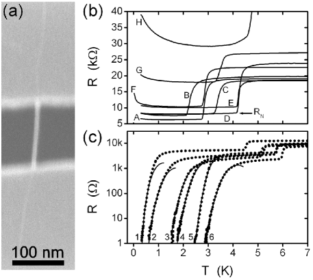
Resistance vs. temperature, , data for insulating and superconducting samples are shown in Figs. 1b and 1c, respectively, where at . The resistive transition observed in all samples at higher temperatures is that of the film electrodes, which are connected in series with the wire. As the electrodes go superconducting, the total sample resistance equals the wire resistance. The only changing parameter amongst all samples is the nominal thickness of MoGe (4.0-8.5 nm). Consistently, the critical temperature of the electrodes decreases gradually as we proceed from the superconducting sample corresponding to the largest amount of MoGe sputtered (sample 6) to the insulating sample with the smallest amount of MoGe sputtered (sample B). The resistance measured immediately below the film transition is taken as the normal (or high-temperature) resistance of the wire, .
The curves of superconducting samples are shown in Fig. 1c. The fits are made using the LAMH-TAPS formulas [20]. As the resistance starts to sharply drop with the cooling, the LAMH model becomes valid, and the data exhibit an excellent agreement with the fits. For the two thinnest samples (1 and 2), which have the lowest ’s, the thermodynamic critical field in the free energy barrier for phase slips had to be modified: We used the empirical expression [30] , instead of the usual . After such modification the fits matched the data. A striking result is that our set of ultrashort wires exhibits an excellent agreement with the TAPS model, without requiring any QPS contribution [7, 10]. This is even true for wires in the vicinity of the SIT. Good agreement with the LAMH model indicates that the observed superconducting regime is a “true” superconducting phase, i.e. the wire resistance is expected to rapidly approach zero as . In this regime, the wires exhibits a negative curvature on ln() vs. plots, which is an indication that the contribution of QPS [7, 10, 19, 21, 31] is negligible. Such QPS-free regime is new and was not seen on longer wires [7, 8, 19, 22].
The curves of nonsuperconducting wires show a qualitatively different behavior (Fig. 1b). We term them “insulating” because they reproducibly show (i) an upturn at the lowest temperatures, i.e. (down to 20 mK, as was tested for sample F), and (ii) a zero-bias resistance peak, i.e. for ( is the bias current and is the bias voltage).
The observed abrupt change from TAPS to the insulating behavior strongly suggests that a quantum phase transition does occur in ultrashort nanowires. This is in contrast to longer wires, which exhibit a crossover [7, 8, 19, 22] from a quasi-superconducting to a quasi-normal regime. We speculate that this SIT takes place due to coupling of QPS to gapless excitations in the environment [11, 13, 14, 15, 16], similar to the Chakravarty-Schmid transition [31, 32, 33, 34]. The QPS-free regime can be understood assuming that the QPS are completely suppressed by a Caldeira-Leggett environment (e.g. produced collectively by the QPS cores). In the insulating phase the QPS proliferate and completely suppress superconductivity, again due to normal cores associated with each QPS.
To understand seen in our insulating samples, we consider the theories of the Coulomb blockade (CB) in diffusive normal wires [23, 24, 35, 36]. Nazarov showed that the CB can survive in a setting in which two plates of a capacitor are connected by a homogeneous normal wire (which now plays the role of a tunnel barrier), even if its resistance is much lower than the von Klitzing constant, , provided that the wire acts as a coherent scatter [23]. Golubev and Zaikin (GZ) [24] derived useful formulas, enabling direct comparisons with experiments. At high temperatures ( , where is the charging energy) the zero-bias conductance, is
| (1) |
where for diffusive wires. Also, , , and is the conductance in the absence of the CB. Apart from the second order term , this result is the same as obtained by Kaupinnen and Pekola for a single tunnel junction [37]. Originally such result was derived for a primary thermometer [38]. The same expression was derived by Joyez and Esteve [39] for a single tunnel junction (i.e. for the dynamic Coulomb blockade), though in their case the value of parameter is defined differently: ( is the impedance of the environment). If the ratio is a small parameter, the diverging terms of the Eq. (1) can be removed by rewriting it as:
| (2) |
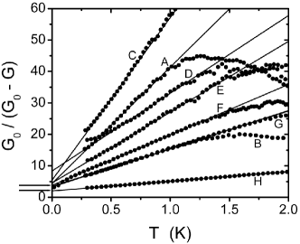
In this form the approximate Eq. (2) follows closely (as our numerical analysis shows) the exact result of GZ given in Eq. (28) in Ref. [24]. In Fig. 2 we replot the data according to Eq. (2). The predicted linearity of the Pekola function is indeed observed on all insulating samples, confirming that CB does occur. The parameter , adjusted to produce the best linearity of the curves, matches the high-bias conductance, as expected (see the caption to Fig. 2). The (Eq. (2)) is determined from the slopes. As indicated by Eq. (2), the offset at should be larger than zero. The arrows in Fig. 2 show the expected range of the offsets, with , which is in a fair agreement with the experiment. At higher temperatures (for example at K for sample A) we observe a deviation from the linear dependence, which might be due to weakening of the proximity effect, induced by the superconducting leads.

At higher bias, the CB appears as a zero-bias anomaly (ZBA) observed in the differential conductance versus bias voltage dependence for all our insulating wires. The anomaly is similar to the one measured by Pekola et al. on single-electron transistors [38]. Examples of ZBA are shown in Fig. 3. We compare the shape of the curves to the GZ theory, in which the ZBA in the dependence is given as
| (3) |
where , , , and is the digamma function. The fitting was done by differentiating Eq. (3) and making an expansion of . The results obtained on high samples agree well with this prediction. On the other hand, for samples near the SIT point (i.e. [31]), the width of the conductance dip was narrower than predicted (Fig. 3a). Since theoretically the resistance peak becomes narrower as increases, the narrowing of the ZBA cannot be explained by an electronic heating, as this would lead to a wider anomaly. Understanding this peak-narrowing effect is difficult because the theory is derived for normal electrodes. We find empirically then that the obtained from Eq. (3) can be used to fit our data with replaced by an effective charge, , which we used as a fitting parameter along with and . With this correction the model matches the experiments. We speculate that the Andreev reflection taking place at the ends of the wire leads to . We also verified that the curves measured at various temperatures show a good agreement with theory (Fig. 3b). Finally, if a perpendicular magnetic field is used to drive the electrodes normal (Fig. 3c), the effective charge decreases to , as expected for all-normal systems. Another explanation for the peak narrowing is the refrigeration effect [40].
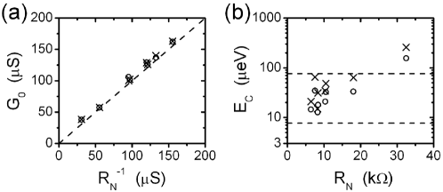
In Figs. 4a and 4b we compare the parameters and obtained from the fits to the plots (measured at 0.3 K) and the same parameters extracted from the fits to the data. A close agreement is observed, thus confirming the consistency of our interpretation. Furthermore, it is clear from Fig. 4a that is very close to for all samples, as it should be.
The extracted from fitting to the and the plots is shown in Fig. 4b as a function of . A strong decrease of with decreasing is seen, possibly due to the renormalization with [23]. The exact physical meaning of the is not well established. One possibility is that the dynamic Coulomb blockade [39] that involves just one barrier (i.e. the entire nanowire) is realized and the effective capacitance is the capacitance between the electrodes (i.e. two coplanar thin films [3]). The relevant sections of the electrodes, which define the effective value of , are determined by a “horizon” [37, 41]. To roughly estimate the charging energy () we calculate the capacitance of the two coplanar plates as , where and is the complete elliptic integral of modulus [42]. For our electrodes of width m, the length m , and the spacing between closest edges m, the capacitance is estimated fF and the corresponding charging energy is eV (top dashed line in Fig. 4b). The lower limit, , was obtained taking into account the capacitance corresponding to the entire area of the electrodes, including the contact pads. Using the program FASTCAP (www.fastfieldsolvers.com) we obtained eV (lower dashed line in Fig. 4b). Most of the experimental values fall between the two limits (Fig. 4b). However, since the length of the studied wires is roughly of the same order as the dephasing length , we note that for wires with there is another model [43], which predicts the same form of as Eq. (2) but uses an effective charging energy that depends only on the wire parameters: [44], where (eV cm)-1 is the density of states of MoGe and is the diameter of a wire. This model gives roughly the same values of the charging energy.
Acknowledgements.
We thank D.S. Golubev and V. Vakaryuk for important discussions and R. Dinsmore for helping with the sample fabrication. This work is supported by NSF CAREER Grant No. DMR 01-34770, DOE grant DEFG02-91-ER45439 that also supports in part our fabrication facilities CMM-UIUC. (∗) Present address: Brookhaven National Laboratory, Upton, NY 11973, USA. (∗∗) Present address: Department of Pysics, University of Utah, Salt Lake City, UT 84112, USA. (∗∗∗) E-mail: bezryadi@uiuc.edu.References
- [1] XIONG P., HERZOG A. V. and DYNES R. C., Phys. Rev. Lett., 78 (1997) 927-930.
- [2] SHARIFI F., HERZOG A. V. and DYNES R. C., Phys. Rev. Lett., 71 (1993) 428-431.
- [3] BEZRYADIN A., LAU C. N. and TINKHAM M., Nature, 404 (1999) 971-974.
- [4] BOLLINGER A. T., ROGACHEV A., REMEIKA and BEZRYADIN A., Phys. Rev. B, 69 (2004) 180503(R).
- [5] ZAIKIN A. D., GOLUBEV D. S., VAN OTTERLO A. and ZIMÁNYI G. T., Usp. Fizich. Nauk., 168 (1998) 244-248.
- [6] FEFAEL G., DEMLER E., OREG Y. and FISHER D. S., cond-mat/0511212 preprint, 2005.
- [7] GIORDANO N. and SHULER E. R., Phys. Rev. Lett., 63 (1989) 2417-2420.
- [8] LAU C. N., MARKOVIC N., BOCKRATH M., BEZRYADIN A. and TINKHAM M., Phys. Rev. Lett., 87 (2001) 217003.
- [9] OREG Y. and FINKEL’STEIN A. M., Phys. Rev. Lett., 83 (1999) 191-194.
- [10] GIORDANO N., Phys. Rev. Lett., 61 (1988) 2137-2140.
- [11] ZAIKIN A. D., GOLUBEV D. S., VAN OTTERLO A. and ZIMÁNYI G. T., Phys. Rev. Lett., 78 (1997) 1552-1555.
- [12] ZAIKIN A. D. and GOLUBEV D. S., Phys. Rev. B, 64 (2001) 014504.
- [13] KHLEBNIKOV S. and PRYADKO, Phys. Rev. Lett., 95, (2005) 107007.
- [14] KHLEBNIKOV S., Phys. Rev. Lett., 93, (2004) 090403.
- [15] FEFAEL G., DEMLER E., OREG Y. and FISHER D. S., Phys. Rev. B, 68 (2003) 214515.
- [16] BÜCHLER H. P., GESHKENBEIN V. B. and BLATTER G., Phys. Rev. Lett., 92 (2004) 067007.
- [17] SACHDEV S., WERNER P. and TROYER M., Phys. Rev. Lett., 92 (2004) 237003.
- [18] LEGGETT A. J., CHAKRAVARTY S., DORSEY A. T., FISHER M. P. A., GARG A. and ZWERGER W., Rev. Mod. Phys., 59 (1987) 1-85.
- [19] ZGIRSKI M., RIIKONEN K. -P., TOUBOLTSEV V., and ARUTYUNOV K., Nano Lett., 5 (2005) 1029-1033.
- [20] ROGACHEV A., BOLLINGER A. T. and BEZRYADIN A., Phys. Rev. Lett., 94 (2005) 017004.
- [21] ROGACHEV A. and BEZRYADIN A., Appl. Phys. Lett., 83 (2003) 512-514.
- [22] TIAN M., WANG J., KURTZ J. S., LIU Y. and CHAN M. H. W., Phys. Rev. B, 71 (2005) 104521.
- [23] NAZAROV Y. V., Phys. Rev. Lett., 82 (1999) 1245-1248.
- [24] GOLUBEV D. S. and ZAIKIN A. D., Phys. Rev. Lett., 86 (2001) 4887-4890.
- [25] LITTLE W. A., Phys. Rev., 156 (1967) 396-403.
- [26] LANGER J. S. and AMBEGAOKAR V., Phys. Rev., 164 (1967) 498-510.
- [27] MCCUMBER D. E. and HALPERIN B. I., Phys. Rev. B, 1 (1970) 1054-1070.
- [28] BEZRYADIN A., BOLLINGER A. T., HOPKINS D., MURPHEY M., REMEIKA M. and ROGACHEV A., Review paper in Dekker Encyclopedia of Nanoscience and Nanotechnology, James A. Schwarz, Cristian I. Contescu, and Karol Putyera, eds. (Marcel Dekker, Inc. New York) 2004, 3761-3774.
- [29] MARTINIS J. M., DEVORET M. H. and CLARKE J., Phys. Rev. B, 35 (1987) 4682-4698.
- [30] TINKHAM M., Introduction to Superconductivity, 2nd ed. (McGraw-Hill, New York) 1996.
- [31] The precision with which the SIT critical point equals the quantum resistance k will be addressed in a separate publication, after a sufficient number of samples is tested.
- [32] CHAKRAVARTY A., Phys. Rev. Lett., 49 (1982) 681-684.
- [33] SCHMID A., Phys. Rev. Lett., 51 (1983) 1506-1509.
- [34] PENTTILÄ J. S., PARTS Ü, HAKONEN P. J., PAALANEN M. A. and SONIN E. B., Phys. Rev. Lett., 82 (1999) 1004-1007.
- [35] WEBER H. B., HÄUSSLER R., LÖHNEYSEN H. v. and KROHA J., Phys. Rev. B, 63 (2001) 165426.
- [36] BECKMANN D., WEBER H. B. and LÖHNEYSEN H. v., Phys. Rev. B, 70 (2004) 033407.
- [37] KAUPPINEN J. P. and PEKOLA J. P., Phys. Rev. Lett., 77 (1996) 3889-3892.
- [38] PEKOLA J. P., HIRVI K. P., KAUPPINEN J. P., and PAALANEN M. A., Phys. Rev. Lett., 73 (1994) 2903- 2906.
- [39] JOYEZ P. and ESTEVE D., Phys. Rev. B, 56 (1997) 1848-1853.
- [40] GIAZOTTO F., HEIKKILA T. T., LUUKANEN A., SAVIN A. M. and PEKOLA J. P., cond-mat/0508093 preprint, 2005.
- [41] CLELAND A. N., SCHMIDT J. M. and CLARKE J., Phys. Rev. Lett., 64 (1990) 1565-1568.
- [42] SONG Y., J. Appl. Phys., 47 (1976) 2651-2655.
- [43] GOLUBEV D. S. and ZAIKIN A. D., Phys. Rev. B, 70 (2004) 165423.
- [44] GOLUBEV D. S., private communication.