Molecular states in a one–electron double quantum dot
Abstract
The transport spectrum of a strongly tunnel-coupled one-electron double quantum dot electrostatically defined in a GaAs/AlGaAs heterostructure is studied. At finite source-drain-voltage we demonstrate the unambiguous identification of the symmetric ground state and the antisymmetric excited state of the double well potential by means of differential conductance measurements. A sizable magnetic field, perpendicular to the two-dimensional electron gas, reduces the extent of the electronic wave-function and thereby decreases the tunnel coupling. A perpendicular magnetic field also modulates the orbital excitation energies in each individual dot. By additionally tuning the asymmetry of the double well potential we can align the chemical potentials of an excited state of one of the quantum dots and the ground state of the other quantum dot. This results in a second anticrossing with a much larger tunnel splitting than the anticrossing involving the two electronic ground states.
keywords:
double quantum dot , single electron tunneling , delocalization , molecular statesPACS:
73.21.La , 73.23.Hk , 73.20.Jc, , , ,
Electrostatically defined semiconductor double quantum dots, where electrons are confined in a double potential well, have recently attracted considerable attention [1]. The interest in these artificial molecules is largely due to the proposed use of quantum dots as spin or charge qubits, the building blocks of the hypothetical quantum computer [2, 3]. Recent works have shown spectacular advancements in reducing the number of electrons trapped in a double quantum dot (DQD) down to [4, 5, 6, 7]. Here we study the transport spectrum of a strongly tunnel-coupled DQD with at finite source-drain voltage . We observe molecule-like hybridization not just between the ground states of both quantum dots, but also at finite potential asymmetry between the ground state of one quantum dot and an excited state of the other dot.
The measurements have been performed on an epitaxially grown AlGaAs/GaAs heterostructure forming a two-dimensional electron system (2DES) below the crystal surface. The electron sheet density in the 2DES is , the electron mobility . We estimate the 2DES electron temperature to be of the order .
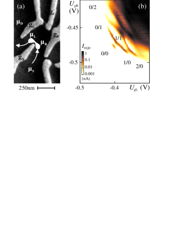
Fig. 1(a) displays an electromicrograph of the gate structure on the crystal surface used to electrostatically define a DQD. The layout is based on the triangular geometry for single quantum dots at very low electron numbers introduced by Ciorga et al. [8]. By tuning the voltages on center gates and to increasingly negative values, we deform the trapping potential in order to create two potential minima shaping a DQD. The approximate geometry of this DQD is indicated in Fig. 1(a) by a white peanut-like shape. Its two quantum dots are strongly tunnel-coupled to each other with a tunnel splitting of typically [6].
Fig. 1(b) displays the dc current through the DQD in linear response () as function of the side gate voltages and . The hexagons of Coulomb blockade typical for transport through a DQD can be recognized [1]. Charge sensing measurements using a nearby quantum point contact provide proof that in the area marked 0/0 the DQD is entirely depleted of conduction band electrons [6]. The subsequent regions of increasing charge in each dot are marked by pairs of numbers , where () is the absolute number of electrons trapped in the left (right) quantum dot. For a weakly tunnel coupled DQD such a stability diagram shows current only at the sharp hexagon corners where three different charge configurations are energetically possible (triple points) [1]. In contrast, in Fig. 1(b) we observe single electron tunnelling (SET) even along the hexagon lines connecting triple points. These resemble not sharp but rounded hexagon corners. This indicates delocalized electronic states due to strong tunnel coupling between the two dots.
In this article, we focus on transport that takes place through one-electron quantum states, i.e. the region of the stability diagram where the charge configurations 0/0, 1/0, and 0/1 are accessible. Fig. 2
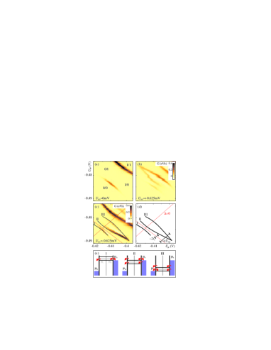
compares the differential conductance of this region of the stability diagram for zero source-drain voltage in (a) with the same region for in (b) and (c). In linear response (Fig. 2(a)) the conductance exhibits the same behaviour as the current shown in Fig. 1(b), i.e. the lines of high current match the local differential conductance maxima (dark lines).
In the case of weak interdot coupling, the triple points of the stability diagram expand at finite source-drain voltage to triangular regions of finite current [1, 9], or a triangle in differential conductance. Here, i.e. for strong tunnel coupling, a more complex structure of three curved lines is observed. The three lines, marked for in Figs. 2(c) and (d) with I, II, and III, correspond to steps in the SET current and indicate that a delocalized quantum level of the DQD is aligned with the chemical potentials of either the source or the drain lead. The detailed situations leading to maximum differential conductance are schematically drawn in Fig. 2(e): Along line I, tunneling through the symmetric ground state of the double well potential becomes accessible, as its energy matches the chemical potential in the source lead (left plot). Line II is caused by an increase in current as the antisymmetric first excited state of the double well potential enters the transport window, providing a second transport channel (middle plot). Along line III the ground state drops below the drain chemical potential (right plot). For even higher gate voltages, the ground state is permanently occupied, such that Coulomb blockade prohibits SET. Since the same quantum state is involved in both cases, lines I and III are parallel to each other.
Obviously, the distance between lines I and II corresponds to the excitation energy , where is the potential asymmetry in the DQD with . In comparison, the distance between lines I and III corresponds to the difference in chemical potential between source and drain contact and provides a known energy scale. Lines I and II depict the anticrossing due to the hybridization of the two orbital ground states of both quantum dots. The solid model lines in Figs. 2(c)–(d) resemble the energy splitting and are obtained using a tunnel splitting of . The model lines have been transformed from the energy to the gate voltage scale by taking into account the geometrical capacitances between gates and quantum dots. The latter were obtained from the slopes of lines of maximum differential conductance similar as in Ref. [6]. Note, that this is a linear transformation, thus, allowing the determination of simply by comparison of the smallest distances between lines I and II versus lines I and III.
At large enough source-drain voltage (large transport window) an additional excited orbital state is observed that decreases in energy with increasing magnetic field perpendicular to the 2DES. This is demonstrated in Fig. 3(a),
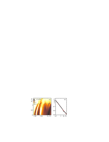
where the differential conductance is plotted as a function of center gate voltage (see Fig. 1(a)) and for a rather large . Gate couples approximately symmetrical to both quantum dots. The side gate voltages and are adjusted such that is provided throughout Fig. 3(a). Lines I, II, and III can be identified with the lines marked respectively in Fig. 2. Between lines II and III an additional line of enhanced differential conductance, marked , becomes visible. It represents a transport channel corresponding to an additional excited orbital state of one of the two quantum dots. The broad dark line at the right edge of the plot marks the onset of tunneling through two-electron states with .
The excitation energy of the excited state causing line corresponds to the distance between the conductance maxima of lines I and . This energy is plotted in Fig. 3(b) as function of the magnetic field for . In this field range line yields an isolated conductance maximum. The solid line depicts suggesting a linear dependence of on the magnetic field [10].
Fig. 4 displays the transport spectrum at the first triple point for mV and .
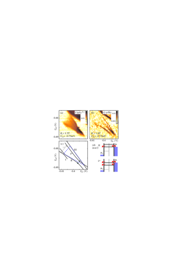
At such a high magnetic field the tunnel splitting caused by the hybridization of both quantum dot ground states is decreased to almost zero because of the increased localization of the orbital wave functions in a perpendicular magnetic field [6] (comp. lines I and II in Fig. 4(c)). Therefore, the region of high current in Fig. 4(a) marking the first triple point of the stability diagram resembles a triangle as expected for electronic states almost localized within the two quantum dots. However, the tip of the triangle seems distorted and shows increased current. The reason for this is revealed by the corresponding differential conductance measurement shown in Fig. 4(b). It depicts an anticrossing of lines II and near the tip of the triangle.
A model describing these observations is plotted in Fig. 4(c). The model lines assume a ground state – ground state tunnel coupling of . An excited orbital state of the left dot (line ) has an excitation energy . It hybridizes with the ground state of the right quantum dot for a potential asymmetry that makes these two states energetically degenerate. Both lines in Fig. 3 and Fig. 4 correspond consistently to the same excited state in the left dot. For a tunnel splitting of , describing the second anticrossing, the model lines of Fig. 4(c) show good agreement with the observed differential conductance maxima. The delocalized states generated by such a hybridization also provide a good explanation for the enhancement of SET as observed in Fig. 4(a). Note, that the tunnel coupling is sizable even for the large magnetic field of . This can be explained in terms of a smaller effective tunnel barrier between the quantum dots for excited orbital states. Possible causes include the higher energy of the excited orbital state or, alternatively, a different orbital symmetry of the excited state, allowing stronger coupling between the quantum dots.
In conclusion, we directly observe anticrossings of molecular states, as a consequence of the quantum mechanical tunnel coupling of one-electron orbital states in two adjacant quantum dots. A conductance measurement at finite source drain voltage reveals the molecular symmetric and antisymmetric states, resulting from the tunnel coupled orbital ground states in both dots, as distinct lines in the stability diagram. A large perpendicular magnetic field quenches this anticrossing. Strikingly, at a large perpendicular magnetic field and finite potential asymmetry we find a second sizable anticrossing between the ground state of one dot and an excited orbital state of the other dot.
We thank R. H. Blick, U. Hartmann, and F. Wilhelm for valuable discussions, and S. Manus for expert technical help, as well as the Deutsche Forschungsgemeinschaft for financial support. A. K. H. thanks the German Nat. Academic Foundation for support.
References
- [1] W. G. van der Wiel, S. D. Franceschi, J. M. Elzerman, T. Fujisawa, S. Tarucha, L. P. Kouwenhoven, Rev. Mod. Phys. 75 (2003) 1.
- [2] D. Loss, D. P. DiVincenzo, Phys. Rev. A 57 (1998) 120.
- [3] W. G. van der Wiel, T. Fujisawa, S. Tarucha, L. P. Kouwenhoven, Jap. J. Appl. Phys. 40 (2001) 2100.
- [4] J. M. Elzerman, R. Hanson, J. S. Greidanus, L. H. W. van Beveren, S. D. Franceschi, L. M. K. Vandersypen, S. Tarucha, L. P. Kouwenhoven, Phys. Rev. B 67 (2003) 161308.
- [5] J. R. Petta, A. C. Johnson, C. M. Marcus, M. P. Hanson, A. C. Gossard, Phys. Rev. Lett. 93 (2004) 186802.
- [6] A. K. Hüttel, S. Ludwig, H. Lorenz, K. Eberl, J. P. Kotthaus, cond-mat/0501012, accepted for publication by Phys. Rev. B (Rapid Comm.) (2005).
- [7] M. Pioro-Ladrière, R. Abolfath, P. Zawadzki, J. Lapointe, S. A. Studenikin, A. S. Sachrajda, P. Hawrylak, cond-mat/0504009 (2005).
- [8] M. Ciorga, A. S. Sachrajda, P. Hawrylak, C. Gould, P. Zawadzki, S. Jullian, Y. Feng, Z. Wasilewski, Phys. Rev. B 61 (2000) 16315.
- [9] A. C. Johnson, J. R. Petta, C. M. Marcus, M. P. Hanson, A. C. Gossard, cond-mat/0410679 (2004).
- [10] The tiny kink in the data course at may be related to the fact that here the two-dimensional electron gas reaches the filling factor , leading to shifts in all line positions.