Spin-charge separation and localization in
one-dimension
O. M. Auslaender,1† H. Steinberg,1 A.
Yacoby,1∗ Y. Tserkovnyak,2 B. I. Halperin,2 K. W.
Baldwin,3 L. N.
Pfeiffer,3 K. W. West3
1Dept. of Condensed Matter Physics, Weizmann
Institute of Science, Rehovot 76100, Israel;
2Lyman Laboratory of Physics, Harvard University, Cambridge, MA 02138, USA;
3Bell Labs, Lucent Technologies,700 Mountain Avenue, Murray Hill, NJ 07974, USA.
†Present address: Geballe Laboratory for Advanced Materials, Stanford University, Stanford, CA 94305, USA.
∗To whom correspondence should be addressed; E-mail: amir.yacoby@weizmann.ac.il.
We report on measurements of quantum many-body modes in ballistic
wires and their dependence on Coulomb interactions, obtained from
tunneling between two parallel wires in a GaAs/AlGaAs
heterostructure while varying electron density. We observe two spin
modes and one charge mode of the coupled wires, and map the
dispersion velocities of the modes down to a critical density, at
which spontaneous localization is observed. Theoretical calculations
of the charge velocity agree well with the data, although they also
predict an additional charge mode that is not observed. The measured
spin velocity is found to be smaller than theoretically predicted.
Coulomb interactions have a profound effect on the behavior of electrons. The low energy properties of interacting electronic systems are described by elementary excitations, which interact with each other only weakly. In two and three-dimensional disordered metals they are dubbed quasi-particles (?), as they bear a strong resemblance to free electrons (?), which are fermions carrying both charge and spin. However, the elementary excitations in one-dimensional (1D) metals, known as Luttinger-liquids (?, ?), are utterly different. Instead, each is collective, highly correlated and carries either spin or charge.
We determine the dispersions of the elementary excitations in one-dimension by measuring the tunneling current, , across an extended junction between two long ballistic parallel wires in a GaAs/AlGaAs heterostructure created by cleaved edge overgrowth (CEO) (?). In this geometry tunneling conserves both energy and momentum. Each tunneling event creates an electron-hole pair with total momentum and total energy , in which is Plank’s constant, is the electron charge, is magnetic field applied perpendicular to the plane of the wires, is the distance between their centers and is the voltage-bias between them (?).
The rate of tunneling between the wires depends on the ease of adding an electron to one wire and a hole to the other, determined by the electron-hole spectral function, . For weak inter-wire interactions, is a convolution of the individual particle spectral functions, which encode the overlap of electrons (or holes) with the many-body modes of the coupled-wires. Near , in the limit of temperature , tunneling is appreciable only if , allowing exchange of electrons between the Fermi-points, , where is electron density in sub-band , while stands for sub-bands in the upper, lower wires. At finite energies, interactions broaden the peaks of the individual particle spectral functions, in particular giving them a distribution of momenta. In spite of this, at , is sharply peaked at for homogeneous wires (?). Thus, as long as momentum is conserved in the wires and in the tunnel junction, tunneling near is enhanced at the same values as without interactions:
| (1) |
For inhomogeneous wires, the line-shape of the spectral function encodes information on the low energy momentum distribution of the many-body states (?).
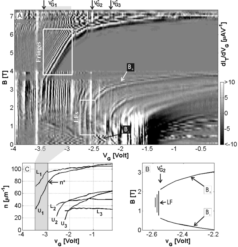
Interactions become more important as the energy associated with them increases relative to kinetic energy. To increase this ratio we reduce electron density in the wires by applying negative voltage, , to a 2 top gate lying on the surface of the device. Figure 1A shows a typical low energy measurement of as a function of and (?). The derivative is measured in order to pick up only the signal from the section of the device where density is controlled by the gate. This is done by adding a small ac component to . A zero-bias anomaly (?, ?) is avoided by setting . This measurement, as well as all those reported here, is performed at 0.25K.
Figure 1B shows the typical behavior of . At high values of , tunneling is appreciable only in a narrow range around . As a function of , evolve continuously, following the behavior of and , allowing us to invert Eq. 1 and extract the density in each sub-band, plotted in Fig. 1C (?, ?). In practice, each wire contains several sub-bands for most of the -range. Tunneling is observed only between sub-bands with the same number of nodes (sub-band #1#1, #2#2 etc.). Tunneling amongst each pair of sub-bands, one sub-band in each wire, gives rise to a similar set of features.
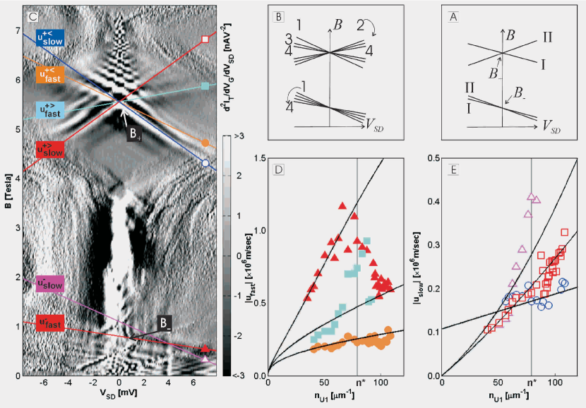
The dispersions of the modes can be determined for every density in the regime where we observe the peaks. The dispersions are traced by the singularities of at finite energy and momentum, as depicted in Figs. 2A,B. For non-interacting electrons, depicted in Fig. 2A, the curves resulting from tunneling either from or to a Fermi-point, produce a total of four curves: two shifted copies of the dispersion in each of the two wires (?).
Finite interactions split the singularities of (Fig. 2B) because of two effects. The first is spin-charge separation, caused by intra-wire interactions, which creates two modes for each non-interacting mode. The second effect is mode-mixing, caused by inter-wire interactions. Generally the mixed modes are carried by both wires, giving rise to four independent velocities (?). This results in three identical copies of each of the four dispersions. In the limit of weak tunneling the spin modes do not couple, and as a result each dispersion branch in Fig. 2A splits into a spin mode and two coupled charge modes, creating four curves near and two sets of three curves near (Fig. 2B).
The tunneling current, , is proportional to , whose singularities are peaks for the parameters of our experiment (?). During a scan of and , changes abruptly when the number of modes that can be excited with the available energy and momentum changes, where is peaked. A curve along which this happens gives the dispersion of a mode, . In particular, the slope at gives the dispersion velocity, . For the experimentally relevant case of weak tunneling we expect ten such intercepts, as shown in Fig. 2B, but only four different magnitudes of slope.
To determine the dependence of the dispersions on density we measured for different ’s, ranging from V to V. A typical result from the regime where each wire has a single sub-band, V, is shown in Fig. 2C. One can see that the peaks that appeared in Fig. 1A at split and move with a slope that gives an apparent velocity: . Accompanying these peaks are finite-size fringes (?).
A total of six slopes appears in Fig. 2C, two near and four near . Both slopes are negative, giving: . Near there are two negative slopes, giving: , and two positive slopes, giving: . For each scan we extracted all discernable slopes. The results are summarized in Figs. 2D,E, where they are plotted versus the density of electrons in the first sub-band of the upper wire, . In the shaded area, which extends up to -1, as extracted from Fig. 1A, only one sub-band is occupied per wire.
The unexpected presence of six different branches of in Figs. 2D,E wrongly suggests that the coupled-wires have more than four independent modes. The error lies in assuming that the band-filling induced by a finite is negligible (?). In reality, induces charge transfer between the wires, which is controlled by the mutual capacitance, endowing and with a -dependence. Thus, the actual excitation velocity is given by:
| (2) |
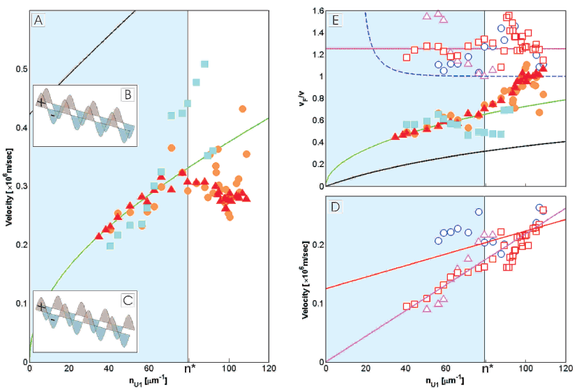
where refers to the crossing point, , near which is extracted. The value of depends on the capacitance matrix of the wires and is calculated using a simple model (?). The model consists of two wires of radius , separated from each other by a distance and from a nearby gate by a distance . Since we apply to the upper wire, keeping the lower wire grounded, the energetic cost of adding charge to the wires is given, to quadratic order in excess electron density, , by , where run over wire indices , is the Fermi-energy, ( is the band mass of electrons, is the Fermi velocity in wire ) and are elements of the inverse capacitance matrix. In the random phase approximation (?), the first term in this expression is kinetic energy, the second is Coulomb interaction energy. By assumption, the inverse-capacitance of each wire to the gate ( and ) is identical: . The inverse-capacitance between the wires is: . Here nm and nm. nm is the distance of the wires to a parallel layer of dopants. Using nm, the distance to the top gate, has only minor influence because of the . The dimensions are roughly MBE growth parameters and were not adjusted. The result of applying Eq. 2 is presented in Fig. 3. Clearly the model is successful when each wire has only one occupied sub-band: all three fast branches collapse on a single curve for and all slow branches collapse on two curves (?).
The same model for interactions, that corrects for band-filling, allows to identify the branches in Fig. 3. For this we turn to the Hamiltonian of the coupled wires, which consists of a free electron part and an interacting part. Taking a long length approximation and bosonizing (?):
| (3) |
The sums run over all occupied sub-bands and over both spin orientations. The density of spin orientation in sub-band is , is the gradient of the displacement operator and is the conjugate momentum.
Within this model, which neglects back-scattering, the velocities of the coupled-wire modes are found by diagonalizing Eq. 3 using a canonical transformation. This yields spin velocities equal to the Fermi-velocities. For a single mode in each wire, , the two charge velocities are (?):
| (4) |
Here are the charge velocities in each individual wire (?): , where is the interaction energy. Physically correspond to symmetric / antisymmetric excitations (illustrated in Figs. 3B,C). When the wires are identical both modes are carried equally by both wires, but when the densities differ, as in the experiment, the symmetric mode is carried primarily by the more occupied wire, the lower wire, while the antisymmetric mode is carried primarily by the upper wire.
We have overlaid the result of Eq. 4 on the corrected velocities in Figs. 3A,E. The fast velocities follow the calculated closely for , attesting to the validity of the model and leading us to associate them with the antisymmetric charge mode. The faster , on the other hand, is completely absent from the data. This is to be expected near , where tunneling creates interacting electron-hole pairs which propagate together, excitations that are almost completely anti-symmetric. On the other hand, near none of the excitations branches should be suppressed, as they are all excited by tunneling, leaving the issue of the complete absence of the symmetric mode unresolved.
Turning to the slow branches in Figs. 3D,E, we find linear dependence on the bare Fermi-velocities, , where . The linearity and the fact that , suggest that these modes are the spin modes. Theoretically one expects a spin velocity equal to as long as back-scattering is small, while finite back-scattering reduces it below (?, ?, ?, ?, ?, ?). For example, one group (?, ?), using Monte Carlo simulations, finds that the expression (?), gives an upper bound to the ratio between the and . However, a plot of in Fig. 3E shows that does not account for the deviation of from unity.
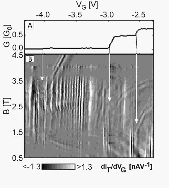
Further examination of Fig. 1A down to the depletion of each sub-band in the upper wire reveals that the continuous evolution of each set of peaks is replaced by a series of vertical streaks, dubbed localization features (LFs). These occur in a small range of below V, for each of the three upper-wire sub-bands we observe. Each set of LFs signals an abrupt change in the momentum-space content of the wavefunction in the depleting sub-band.
Above finite-size fringes for and accompany the -peaks, signifying that the states in both wires contain only wavenumbers higher than the Fermi wavenumber and implying that they are extended (?). The location of the fringes at and indicates that the potential along the non-uniform upper wire has a hump, with a typical length given by the period: , consistent with the barrier the surface gate induces.
Below , we find that each LF fills a broad range in , lying roughly between the extrapolations of . This implies that the wavefunction of the state along the upper wire is localized. We are thus led to conclude that the -streaks signify a qualitative change in the self-consistent potential at , which marks a transition between an extended state and a localized state. The localized states appear while the more occupied sub-bands are still fully conducting, in contrast to a recent study of inhomogeneous wires (?).
The localization transition affects transport along the upper wire. Figure 4A shows the two-terminal conductance along this wire, , which is quantized. The stepwise decrease of with density is a hallmark of ballistic transport in a wire (?). We were able to measure simultaneously with , by recording both the dc-current along the upper wire and the ac-component of the tunneling current (?). The positions of the steps in , whose dependance on is very weak, are concurrent with the localization transitions apparent in Fig. 4B. We thus conclude that electrons in a sub-band cease to conduct because of localization while their density is still finite.
The localization transition hints that bound states come into existence over the barrier induced by the top gate, which we use to vary the density. The possibility of this occurring has been addressed in the context of the 0.7-anomaly in point contacts (?, ?, ?, ?). Using a variety of theoretical tools it was found that, when the density is low enough, a bound state may exist over the barrier (?, ?, ?, ?). Our measurements show clear evidence for this scenario in long 1D channels. Finally, 0.7-anomaly-like features are observed regularly in the conductance steps of CEO wires similar to ours (?). Further work is needed to show a direct link between the -anomaly and the observed localization features.
References and Notes
- 1. P. Nozières, D. Pines, The Theory of Quantum Liquids, The Advanced Book Program (Perseus Books, Cambridge, MA, 1999), third edn.
- 2. B. L. Altshuler, A. G. Aronov, Electron–Electron Interaction in Disordered Systems, A. L. Efros, M. Pollak, eds. (North-Holland, Amsterdam, 1985), pp. 1–153.
- 3. S.-I. Tomonaga, Prog. of Theor. Phys. 5, 544 (1950).
- 4. J. M. Luttinger, J. Math. Phys. 4, 1154 (1963).
- 5. O. M. Auslaender, et al., Science 295, 825 (2002).
- 6. See supporting text.
- 7. D. Carpentier, C. Peça, L. Balents, Phys. Rev. B 66, 153304 (2002).
- 8. Y. Tserkovnyak, B. I. Halperin, O. M. Auslaender, A. Yacoby, Phys. Rev. B 68, 125312 (2003).
- 9. Y. Tserkovnyak, B. I. Halperin, O. M. Auslaender, A. Yacoby, Phys. Rev. Lett. 89, 136805 (2002).
- 10. D. Boese, M. Governale, A. Rosch, U. Zülicke, Phys. Rev. B 64, 085315 (2001).
- 11. K. A. Matveev, L. I. Glazman, Phys. Rev. Lett. 70, 990 (1993).
- 12. C. L. Kane, M. P. A. Fisher, Phys. Rev. B 46, 15233 (1992).
- 13. C. F. Coll, Phys. Rev. B 9, 2150 (1974).
- 14. H. J. Schulz, Phys. Rev. Lett. 71, 1864 (1993).
- 15. C. E. Creffield, W. Häusler, A. H. MacDonald, Europhys. Lett. 53, 221 (2001).
- 16. W. Häusler, L. Kecke, A. H. MacDonald, Phys. Rev. B 65, 085104 (2002).
- 17. K. A. Matveev, Phys. Rev. Lett. 92, 106801 (2004).
- 18. V. V. Cheianov, M. B. Zvonarev, Phys. Rev. Lett. 92, 176401 (2004).
- 19. K. J. Thomas, et al., J. Phys.: Condens. Matter 16, L279 (2004).
- 20. C. W. J. Beenakker, H. van Houten, Solid State Physics, Semiconductor Heterostructures and Nanostructures, H. Ehrenreich, D. Turnbull, eds. (Academic Press, New York, 1991).
- 21. K. J. Thomas, et al., Phys. Rev. Lett. 77, 135 (1996).
- 22. S. M. Cronenwett, et al., Phys. Rev. Lett. 88, 226805 (2002).
- 23. D. J. Reilly, et al., Phys. Rev. Lett. 89, 246801 (2002).
- 24. R. de Picciotto, L. N. Pfeiffer, K. W. Baldwin, K. W. West, Phys. Rev. Lett. 92, 036805 (2004).
- 25. Y. Meir, K. Hirose, N. S. Wingreen, Phys. Rev. Lett. 89, 196802 (2002).
- 26. K. Hirose, Y. Meir, N. S. Wingreen, Phys. Rev. Lett. 90, 026804 (2003).
- 27. O. P. Sushkov, Phys. Rev. B 67, 195318 (2003).
- 28. A. Yacoby, et al., Phys. Rev. Lett. 77, 4612 (1996).
- 29. R. de Picciotto, H. L. Stormer, L. N. Pfeiffer, K. W. Baldwin, K. W. West, Nature 411, 51 (2001).
-
1.
With pleasure we acknowledge numerous discussions with Greg Fiete, Yuval Oreg and Jiang Qian. This work was supported in part by the US-Israel BSF, the European Commission RTN Network Contract No. HPRN-CT-2000-00125 and NSF Grant DMR 02-33773. YT is supported by the Harvard Society of Fellows.
Supporting text
The actual values of the charge velocity, , and the spin velocity, , depend on microscopic details and are very difficult to determine, both theoretically and in experiment. Of particular interest is their dependence on , which directly controls the ratio between the Coulomb interaction and kinetic energy. A one-dimensional charge mode, which resembles a charge density wave, travels with a velocity that is strongly affected by the Coulomb interaction: . Here the Fermi-velocity is a measure of electron density and is a measure the relative strength of the Coulomb interaction. For repulsive interactions , while for non-interacting electrons . Within the random phase approximation, which gives reliable estimates for if backscattering is weak, it is found that as is reduced, decreases.
The propagation velocity of the spin modes, , is related to exchange interaction. According to theory, is suppressed for very strong repulsive interactions, where it is difficult for adjacent electrons to exchange places, leading to (?, ?, ?, ?). The main text cites an example for the suppression factor of relative to in one model (?, ?), which is given by . Here is the Fourier transform of the two-body interaction potential in a single wire in the presence of a gate. It is given by:
where is a Bessel function, is the Bohr radius in GaAs and is the distance to the top gate, nm.
A remark is due on the number of expected singularity branches crossing the axis in a measurement of . In principle, even in the absence of inter-wire interactions, we expect for each charge mode an extra feature with opposite slope and very small amplitude (unless interactions are very strong). This gives an extra copy of each charge mode branch near . The reason is that forward scattering has a contribution from interactions between left and right movers, causing an electron tunneling into one branch of movers to induce a density modulation in the other branch as well.
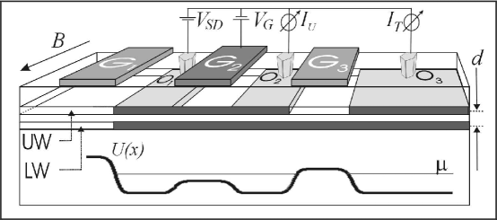
Our device consists of two parallel wires separated by a tunnel junction at the edges of two quantum wells in a GaAs/AlGaAs heterostructure created by cleaved edge overgrowth (?). The band structure is such that besides the wires along the edge, the upper well is also occupied by a two-dimensional electron gas (2DEG), which we use to contact the wires. The measurements were conducted in a 3He-fridge at a base temperature of K. After the sample cools down, it is illuminated by infra-red light, which ionizes impurities and increases the overall electron density in the device.
Tungsten top-gates, 2-wide, lying nm above the tunnel junction and 2 apart, control the density in sections of the device. Both the tunnel junction and the upper wire are delimited by applying voltage to two peripheral gates, G1 & G3 in Fig. S1, lying 10 apart. Bias voltage is applied to a central gate, G2 in Fig. S1, to vary the density in the central section of the device. To increase sensitivity to processes affected by G2, we measure the derivative of with respect to . To this end we add a small ac-component to (a few mV at a few Hz), apply finite to contact O1 and pick up the resulting current at contact O3 with a lock-in amplifier. An additional contact, O2, can be grounded in order to measure the current along the upper wire, , but is left floating otherwise. To measure we apply voltage to contact O1 (cf. Fig. S1) and ground contact O2. This gives net bias relative to the lower wire (where ) and a bias drop of along the upper wire.
In the -range being studied we do not observe transitions between a sub-band in one wire and more than one sub-band in the other wire. This hints at a selection rule, which we conjecture arises from the similarity of the wavefunctions in the two wires in the planes perpendicular to them (?). According to the rule, the overlap of wavefunctions in different wires with a different number of nodes perpendicular to the wires is small and suppresses the transitions between them. In identical wires this selection rule would be absolute, because wavefunctions from different sub-bands would be orthogonal.
The finite width of the wires in the direction perpendicular to distorts the dispersions slightly. Equation 1 in the main text is precise only as long as a single sub-band is occupied in each wire. When higher sub-bands are occupied, finite flattens the dispersions (?), changing the occupations and generally making it energetically favorable to occupy lower sub-bands at the expense of higher ones. We ignore this distortion as it gives an error that is comparable to the accuracy of the measurement.
In the main text we describe a model that allows to calculate the actual excitation velocities from the measured slopes. According to the model, the value of appearing in Eq. 2 in the main text is given by:
| (S1) |
where , while the rest of the quantities here are given in the main text.
The model has a limited range of validity. Above , as more sub-bands are occupied, it exaggerates the voltage-induced band-filling. In this regime, the sparsely occupied sub-bands are filled instead of the more populated ones, because they are more compressible. Thus in this regime Eq. 2 corrects the ’s too much, bringing the corrected velocities too low, as can be seen for , in Fig. 3. To obtain the fits shown in this figure we used the same values of and as for the band-filling correction. For we used here nm, the distance to the metallic top gate, rather than the distance to the dopant layer, because typical timescales for the reaction of that layer are too slow to influence the dynamics of the modes.
References and Notes
- S1. H. J. Schulz, Phys. Rev. Lett. 71, 1864 (1993).
- S2. W. Häusler, L. Kecke, A. H. MacDonald, Phys. Rev. B 65, 085104 (2002).
- S3. K. A. Matveev, Phys. Rev. Lett. 92, 106801 (2004).
- S4. V. V. Cheianov, M. B. Zvonarev, Phys. Rev. Lett. 92, 176401 (2004).
- S5. C. E. Creffield, W. Häusler, A. H. MacDonald, Europhys. Lett. 53, 221 (2001s).
- S6. O. M. Auslaender, et al., Science 295, 825 (2002).
- S7. Y. Tserkovnyak, B. I. Halperin, O. M. Auslaender, A. Yacoby, Phys. Rev. B 68, 125312 (2003).
- S8. K. F. Berggren, T. J. Thornton, D. J. Newson, M. Pepper, Phys. Rev. Lett. 57, 1769 (1986).