Tight-Binding model for semiconductor nanostructures
Abstract
An empirical tight-binding (TB) model is applied to the investigation of electronic states in semiconductor quantum dots. A basis set of three -orbitals at the anions and one -orbital at the cations is chosen. Matrix elements up to the second nearest neighbors and the spin-orbit coupling are included in our TB-model. The parametrization is chosen so that the effective masses, the spin-orbit-splitting and the gap energy of the bulk CdSe and ZnSe are reproduced. Within this reduced TB-basis the valence (p-) bands are excellently reproduced and the conduction (s-) band is well reproduced close to the -point, i.e. near to the band gap. In terms of this model much larger systems can be described than within a (more realistic) -basis. The quantum dot is modelled by using the (bulk) TB-parameters for the particular material at those sites occupied by atoms of this material. Within this TB-model we study pyramidal-shaped CdSe quantum dots embedded in a ZnSe matrix and free spherical CdSe quantum dots (nanocrystals). Strain-effects are included by using an appropriate model strain field. Within the TB-model, the strain-effects can be artifically switched off to investigate the infuence of strain on the bound electronic states and, in particular, their spatial orientation. The theoretical results for spherical nanocrystals are compared with data from tunneling spectroscopy and optical experiments. Furthermore the influence of the spin-orbit coupling is investigated.
pacs:
73.22.Dj, 68.65.Hb, 71.15.ApI Introduction
Semiconductor quantum dots Woggon (1997); Michler (2000) (QDs) are of particular interest, both concerning basic research and possible applications. QDs are considered to be zero dimensional objects, i.e. systems confined in all three directions of space with a typical size of the magnitude of several nanometers. Therefore, these systems are realizations of “artificial atoms” whose form and size can be manipulated. Concerning basic research these nanostructures (QDs) are interesting, as the methods of quantum theory can be applied to systems on new scales and with new symmetries in between that of atoms or molecules and of macroscopic crystals. On the other side light emission and absorption just from the localized states in such devices may be important for optoelectronic applications Passaseo et al. (2001); Grundmann (2002), quantum cryptography Michler et al. (2000) and quantum computing Li et al. (2003).
Semiconductor QDs can be realized by means of metallic gates
providing external (electrostatic) confinement
potentials van der Wiel et al. (2003), by means of selforganized
clustering of certain atoms in the Stranski-Krastanow (SK) growth
mode Merz et al. (1998); Yang et al. (2001); Zhang et al. (2001) or chemically by stopping
the crystallographic growth using suitable surfactant
materials Kim et al. (2001); Guzelian et al. (1996); Manna et al. (2000); Murray et al. (2001). Here we
deal only with the latter two types of QDs. The QDs created in the
SK growth mode emerge self-assembled or self-organized in the
epitaxial growth process because of the preferential deposition of
material in regions of intrinsic strain or along certain
crystallographic directions. In epitaxial growth of a semiconductor
material A on top of a semiconductor material B only one or a few
monolayers of A material may be deposited homogeneously as a quasi
two dimensional (2d) A-layer on top of the B-surface forming the so
called wetting layer (WL). Under certain conditions and for certain
materials further deposited A-atoms will not form a further
homogeneous layer but they will cluster and form islands of
A-material because this may lower the elastic energy due to the
lattice mismatch of the A- and B-material. If one then stops the
growth process, one has free A-QDs on top of an A-WL on the
B-material. If one continues the epitaxial growth process with
B-material, one obtains embedded quantum dots (EQDs), i.e. QDs of
A-material on top of an A-WL embedded within B-material.
The chemically realized QDs emerge
by means of colloidal chemical
synthesis Kim et al. (2001); Guzelian et al. (1996). Thereby the crystal growth of
semiconductor material in the surrounding of soap-like films called
surfactants is stopped when the surface is covered by a monolayer of
surfactant material. Thus one obtains tiny crystallites of the
nanometer size in all three directions of space, why these QDs are
also called “nanocrystals” (NCs). The size and the shape of the
grown NCs can be controlled by external parameters like growth time,
temperature, concentration and surfactant
material Manna et al. (2000); Murray et al. (2001). Certain physical properties
like the band gap (and thus the color) depend crucially on the size
of the NCs. Typical diameters for both, EQDs and NCs, are between 3
and 30 nm, i.e. they contain between up to atoms.
Therefore, EQDs and NCs can be considered to be a new, artficial
kind of condensed matter in between molecules and solids. For the in
SK-modus grown EQDs lens-shaped dots Wojs et al. (1996), dome shaped and
pyramidal dots Fry et al. (2000); Ruvimov et al. (1995); Merz et al. (1998), and also truncated
cones Shumway et al. (2001) have been found and considered.
Of course the fundamental task is the calculation of the electronic properties of EQDs and NCs. But here one encounters the difficulty that these systems are much larger than conventional molecules and that the fundamental symmetry of solid state physics, namely translational invariance, is not fulfilled. Therefore, neither the standard methods of theoretical chemistry nor the ones of solid state theory can immediately be applied to systems with up to atoms. Conventional ab-initio methods of solid state theory based on density functional theory (DFT) and local density approximation (LDA) would require supercell calculations. But the size of a supercell must be larger than the EQD or NC, and such large supercells are still beyond the possibility of present day computational equipment. Therefore, only systems with up to a few hundred atoms can be investigated in the framework of the standard ab-initio DFT methods Puzder et al. (2004); Sarkar and Springborg (2003); Deglmann et al. (2002). Simple model studies based on the effective mass approximation Wojs et al. (1996); Grundmann et al. (1995) or a multi-band -model Stier et al. (1998); Fonoberov and Baladin (2003); Pryor (1998) describe the QD by a confinement potential caused by the band offsets, for instance; they give qualitative insights into the formation of bound (hole and electron) states, but they are too crude for quantitative, material specific results or predictions. More suitable for a microscopic description are empirical pseudopotential methods Wang et al. (1999, 2000); Williamson et al. (2000); Kim et al. (1998) as well as empirical tight-binding models Saito and Arakawa (2002); Lee et al. (2001, 2002); Allan et al. (2000); Niquet et al. (2001); Santoprete et al. (2003); Hill and Whaley (1994); Leung et al. (1998); Leung and Whaley (1999); Pokrant and Whaley (1999); Schrier and Whaley (2003); Lee et al. (2004). The empirical pseudopotential methods allow for a detailed variation of the wave functions on the atomic scale. This is certainly the most accurate description from a microscopic, atomistic viewpoint, but it requires a large set of basis states. Within a TB-model some kind of coarse graining is made and one studies spatial variations only on inter-atomic scales and no longer within one unit cell. The advantage is that usually a small basis set is sufficient, which allows for the possibility to study larger systems. Furthermore the TB-model provides a simple physical picture in terms of the atomic orbitals and on-site and inter-site matrix elements between these orbitals. A cutoff after a few neighbor shells is usually justified for orbitals localized at the atomic sites.
Semiempirical TB-models have been used already to describe ”nearly” spherical InAs and CdSe NCs for which the dangling bonds at the surfaces are saturated by hydrogen Lee et al. (2001, 2002); Niquet et al. (2001); Allan et al. (2000) or organic ligands Leung et al. (1998); Leung and Whaley (1999); Pokrant and Whaley (1999). Also uncapped Saito et al. (1998) and capped Santoprete et al. (2003) pyramidal InAs QDs were ivestigated by use of an empirical TB-model. In the latter work an -basis was used leading to a Hamiltonian matrix, where is the number of atoms, with 33 independent parameters. In the present paper we apply a similar TB-model to II-VI nanostructures, namely CdSe EQDs embedded within ZnSe and spherical CdSe NCs. We show that a smaller TB-basis is sufficient, namely an -basis, i.e. 4 states per unit cell and spin direction. This requires only 8 independent parameters and, in principle, allows for the investigation of larger nanostructures than were accessible in Ref. Santoprete et al., 2003. Strictly speaking, the -basis-set leads to a smaller matrix-dimension and also to a smaller number of nonzero matrix elements compared to TB-model. So the TB-model is numerically less demanding regarding both memory requirements and computational time. For the bulk system the valence p-bands are excellently reproduced and the conduction s-band is well reproduced close to the -point. Therefore, we expect that also for the QDs all the hole states and at least the lowest lying electron states (close to the gap) are well reproduced. We investigate, in particular, the influence of strain effects on the electronic structure. To examine the accuracy of our model we compare the results to other microscopic and macroscopic models. Furthermore TB-results obtained for CdSe-NCs are compared to experimental results, and very good agreement, for instance for the dependence of the energy gap on the NC-diameter, is obtained. This demonstrates that our TB-model with a reduced basis set is reliable and sufficient for the reproduction of the most essential electronic properties of the nanostructures.
| CdSe | ZnSe | |
|---|---|---|
| [eV] | 1.74 Kim et al. (1994) | 2.8201 Kim et al. (1994) |
| [eV] | 0.41 Kim et al. (1994) | 0.43 Kim et al. (1994) |
| 0.12 Kim et al. (1994) | 0.147 Hölscher et al. (1985) | |
| 3.33 Kim et al. (1994) | 2.45 Hölscher et al. (1985) | |
| 1.11 Kim et al. (1994) | 0.61 Hölscher et al. (1985) | |
| 1.45 Kim et al. (1994) | 1.11 Hölscher et al. (1985) | |
| [GPa] | 46.3 Pellegrini et al. (1995) | 50.6 Pellegrini et al. (1995) |
| [GPa] | 66.7 Pellegrini et al. (1995) | 85.9 Pellegrini et al. (1995) |
This work is organized as follows. In Sec. II our TB-model is presented. The formalism how to obtain the TB-parameters and how to apply them to the description of EQDs and NCs is described. In Sec. III the inclusion of strain effects in our model is introduced. Results for the pyramidal CdSe EQDs are presented. For the spherical CdSe NCs the results and the comparison with the experimental data are presented in Sec. IV. Section V contains a summary and a conclusion.
II Theory
II.1 TB-Model for bulk materials
In this work we use a TB-Model with 8 basis states per unit cell. Such a model has been succesfully used for the investigation of optical properties in ZnSe-quantum wells Dierks and Czycholl (1998). For the description of the bulk semiconductor compounds CdSe and ZnSe we choose an basis set. That implies that the set of basis states is given by four orbitals with spin . One -orbital at the cation () and three -orbitals at the anion () site in each unit cell are chosen. The TB matrix elements are given by
| (1) |
The coupling of the basis orbitals is limited to nearest and next
nearest neighbors. Following Ref. Chadi, 1977, the spin-orbit
component of the bulk Hamiltonian couples only
orbitals at the same atom. With the two center approximation of
Slater and Koster Slater and Koster (1954) we are left with only 8
independent matrix elements .
In space, with the basis states
, the electronic properties of
the pure bulk material are modelled by an matrix
(for each from the
first Brillouin zone). This matrix depends on the different
TB-parameters .
By analytical diagonalization for special directions, the
electronic dispersion is obtained as a function of
the TB-parameters; here is the band index. Equations for the
different TB-parameters
can now be
deduced as a function of the Kohn-Luttinger-parameters
(,,), the energy gap ,
the effective electron mass and the spin-orbit-splitting
. The zero level of the energy scale is fixed to
the valence-band maximum. The used material parameters for CdSe and
ZnSe are given in Table 1. The resulting
numerical values for the different TB-parameters (obtained by
optimizing them so that the resulting TB band-structure reproduces
the parameters given in Table 1) are summarized
in the Table 2 (with and without taking into
account a site-diagonal parameter for the spin-orbit coupling).
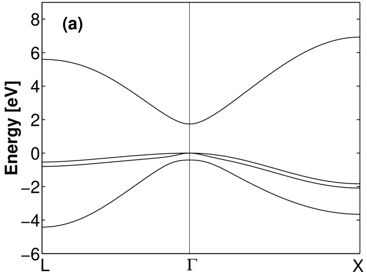
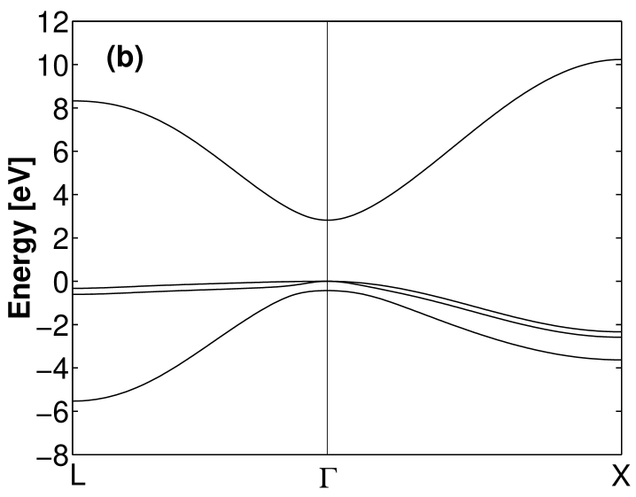
Within this approach, the characteristic properties of the band
structure in the region of the point are well reproduced,
as can be seen from Fig. 1, which shows the
TB-bands of bulk CdSe and ZnSe (using the TB-parameters with
spin-orbit coupling). When comparing with band structure results
from the literatureCohen and Chelikowski (1989), one sees that the three valence
(-) bands are excellently reproduced whereas the -like
conduction band is well reproduced only close to the -point.
This is understandable, because higher (unoccupied) conduction bands
are neglected, and can be improved by taking into account more basis
states per unit cell. But for a reproduction of the electronic
properties in the region near the -point, which is important
for a proper description of the optical properties of the
semiconductor materials, the -TB-model is certainly
sufficient and satisfactory.
| Material | Parameter | TB | TB-NO SO |
|---|---|---|---|
| ZnSe | -1.7277 | -2.0413 | |
| 7.0462 | 12.1223 | ||
| 1.1581 | 0.2990 | ||
| 0.1044 | 0.2185 | ||
| 0.1874 | 0.0732 | ||
| 0.3143 | 0.4285 | ||
| -0.3522 | -0.7752 | ||
| 0.1433 | 0 | ||
| CdSe | -1.2738 | -1.7805 | |
| 3.6697 | 10.8053 | ||
| 1.1396 | 0.4260 | ||
| 0.0552 | 0.2161 | ||
| 0.1738 | 0.0129 | ||
| 0.1512 | 0.3120 | ||
| -0.1608 | -0.7554 | ||
| 0.1367 | 0 |
II.2 TB-Model for Embedded Quantum Dots and Nanocrystals
Having determined suitable TB-parameters for the bulk materials (here CdSe and ZnSe) a EQD or NC can be modelled simply by using the TB-parameters of the bulk materials for those sites (or unit cells) occupied by atoms (or molecules) of this material. Concerning the on-site matrix elements this condition is unambiguous. Concerning the intersite matrix elements one also uses the bulk matrix elements, if the two sites are occupied by the same kind of material, but one has to use suitable averages of the bulk intersite matrix elements for matrix elements over interfaces between different material, i.e. if the two sites (or unit cells) are occupied by different atoms (or molecules). Concerning the surfaces or boundaries of the nanostructure there are different possibilities. One can use fixed boundary conditions, i.e. effectively use zero for the hopping matrix elements from a surface atom to its fictitious nearest neighbors, or (for the embedded QDs) one can use periodic boundary conditions to avoid any surface effects, which artificially arise from the finite cell size used for the EQD-modelling. For the NCs the best thing to do is a realistic, atomistic modelling of the organic ligands covering the NC-surface, as described in Refs.Pokrant and Whaley (1999); Rabani (2003); Puzder et al. (2003). Within the restricted basis set thus selected the ansatz for an electronic eigenstate of the EQD or NC is, of course, a linear combination of the atomic orbitals :
| (2) |
Here denotes the unit cell, the orbital type, the spin and an anion or cation. Then the Schrödinger equation leads to the following finite matrix eigenvalue problem:
| (3) |
where is the energy eigenvalue. The shortcut notation is used in the following for the matrix elements with and .
The matrix elements for CdSe and ZnSe without strain are denoted by . For these matrix elements the TB-parameters of the bulk materials, determined in Sec. II.1, are used. For the off-diagonal matrix elements over interfaces and the diagonal matrix elements of the selen atoms at the interface between dot and barrier, which can not unambiguously be referred to belong to the ZnSe or CdSe, respectively, we choose the mean value of the parameters for the two materials. Furthermore, a parameter for the valence-band offset has to be included in the model. This means that for CdSe in a heterostructure, i.e. surrounded by a barrier ZnSe material, all diagonal matrix elements are shifted just by compared to the bulk CdSe diagonal matrix elements. In the literature different values for can be found, they vary in the range of 10 %-30 % of the band gap difference between CdSe and ZnSe Kurtz et al. (2001); Yang et al. (2001); Lakes et al. (1996). We have performed calculations with valence-band offsets of eV, eV and eV, which corresponds to 10 %, 20 % and 30 % of the difference of the band gaps. We find that these different choices for shift the EQD energy gap by less than 2 %. This shows, that the results are not much affected by the specific choice of the valence-band offset . Therefore, in the following, an intermediate value of eV is chosen.
Furthermore, in a heterostructure of two materials with different lattice constants, strain effects have to be included for a realistic description of the electronic states, because the distance between two CdSe unit cells and the bond angles are not the same as the corresponding equilibrium values in bulk CdSe. This means that the intersite TB matrix elements in the EQD differ from the matrix elements in the bulk material. In general, a relation
| (4) |
has to be expected, where and are the bond vectors between the atomic positions of the unstrained and strained material, respectively. The function describes, in general, the influence of the bond length and the bond angle on the intersite (hopping) matrix elements. For lack of a microscopic theory for the functional form we use as a simplified model assumption . With this ansatz, the interatomic matrix elements , with , are given by
| (5) |
This corresponds to Harrison’s Froyen and Harrison (1979) rule, the validity of which has been demonstrated for II-VI-materials by Sapra et al. Sapra et al. (2002). More sophisticated ways to treat the scaling of the interatomic matrix elements, e.g. by calculating the dependence of energy bands on volume effects and different exponents for different orbitals, can be found in the literature Jancu et al. (1998); Santoprete et al. (2003); Lee et al. (2004). Furthermore the results of Bertho et al. Bertho et al. (1991) for the calculations of hydrostatic and uniaxial deformation potentials in case of ZnSe show that the rule should be a reasonable approximation. Our model assumption for the function means that we neglect the influence of bond angle distortion. Though energy shifts due to bond angle distortions have been found for InAs EQDsSantoprete et al. (2003), here the negligence of bond angle distortion can be justified when exclusively taking into account the coupling between s- and p-orbitals at nearest neighbor sites. Piezoelectric fields, which are usually considered to be less important for the zinc blende structures realized in CdSe and ZnSe Fonoberov and Baladin (2003), are also not taken into account in our model.
III Results for a pyramidal Embedded Quantum Dot
III.1 Geometry and Strain
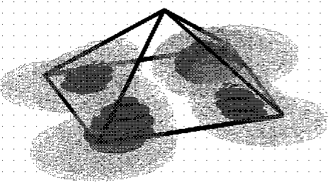
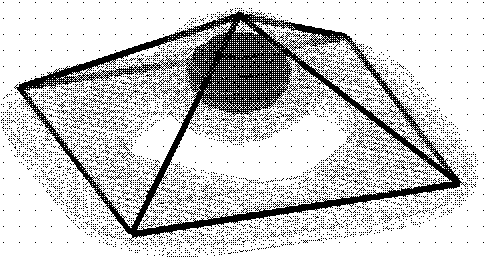
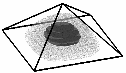
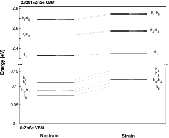
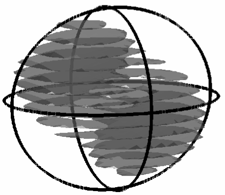
To model a CdSe QD embedded into a ZnSe barrier material we choose a finite (zinc blende) lattice within a box with fixed boundary conditions. Within this box we consider a CdSe WL of thickness (lattice constant of the conventional unit cell, i.e. about two anion and two cation layers), and on top of this wetting layer there is a pyramidal QD with base length and height . For the matrix elements corresponding to sites within the WL or the QD we choose the TB-values appropriate for CdSe, for all other sites within the box the ones for ZnSe. Figure 2 shows a schematic picture of this geometry we use to model the EQD. We investigate EQDs with a base lengths of , and , where is the lattice constant of the bulk ZnSe material. Cells with the dimensions of (38 880 atoms), (51 200 atoms) and (65 824 atoms) are used for the calculations.
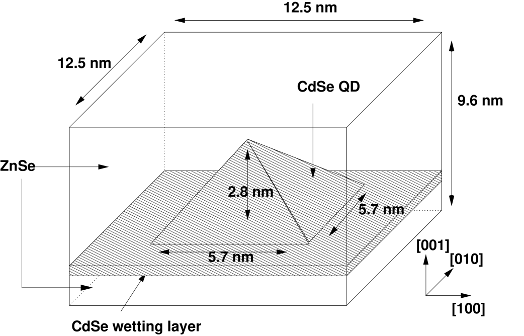
Figure 2 shows the EQD with a base length of . Fixed boundary conditions are applied to avoid a dot-dot coupling in contrast to periodic boundary conditions Santoprete et al. (2003). The total size of the cells is chosen so that the boundary conditions affect the energy gap of the EQD by less than 2 %.
To consider strain effects in our model the knowledge of the strain tensor is necessary. The strain tensor is related to the strain dependend relative atomic positions by
| (6) |
To appoint the strain tensor outside the EQD, the WL is treated as a quantum film. In the absence of a shear strain () for a coherently grown film, the strain components are given by Chuang (1995)
| (7) | |||||
| (8) |
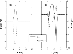
Here is the lattice constant of the unstrained film material and denotes the parallel lattice constant of the substrate. In Table 1 the cubic elastic constants of the bulk materials are given. The resulting strain profile for a line scan in z-direction outside the dot is shown in Fig. 3 (a). In Ref. Stier et al., 1998 Stier et al. considered a similar strain profile for an InAs/GaAs EQD. The lattice mismatch of approximately 7 % in the InAs/GaAs system is nearly the same as for the CdSe/ZnSe system. So our calculated strain profile shows the same behavior as the profile in Ref. Stier et al., 1998 for a line scan in z-direction outside the EQD.
To obtain the strain profile inside the EQD we use a model strain profile, which shows a similar behavior as the strain profiles which are given in Refs. Pryor et al., 1998; Stier et al., 1998 for a line scan in z-direction through the tip of the pyramid. This model strain profile is displayed in Fig. 3 (b). The shear components, , and , can be neglected, at least away from the boundaries of the dot Grundmann et al. (1995).
III.2 Bound single particle states
We have calculated the first five states for electrons and holes for
three different EQD sizes. These calculations are done with and
without including strain effects. For the evaluations without strain
we have chosen the exponent in Eq. (5) to be
zero. The energy spectrum obtained from these calculations is shown
in Fig. 4 (a) without strain and in
Fig. 4 (b) including strain effects. The states
are labeled by and for electron and hole ground states,
and for the first excited states, and so on. All
energies are measured relative to the valence-band maximum of ZnSe.
Figure 4 also shows the size dependence of the
electron and hole energy levels. The energies are compared to the
ground state energies for electrons and holes in the thick
CdSe WL ( and , respectively),
which is calculated separately for a coherently strained quantum
film (i.e. the WL without the QD). As expected from a naive particle
in a box picture, the binding of electrons and holes becomes
stronger in the EQD when the dot size is increased. The quantum
confinement causes the number of bound states to decrease when the
dot size is reduced. For the EQDs with a base length and
the calucated hole states are well above the WL energy
(). This is valid for the strain-unaffected and
strained EQD. For the system with we obtain at least four
bound hole states in both models. The energy splitting between the
different states is only slightly influenced by the strain.
Furthermore we see from Fig. 4 that the number of
bound electron states is influenced by the strain. For the system
with a base length of we get at least three bound-electron
states when we take strain effects into account
(Fig. 4 (b)). Without strain effects at least 5
bound states are found. So the confinement potential for the
electrons is effectively
reduced by the strain.
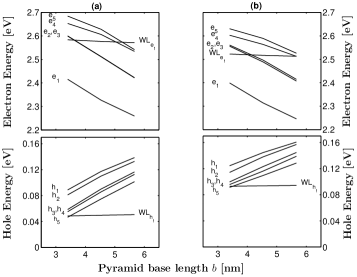
The bound electron states and are energetically not degenerate even without strain. This arises from the symmetry of the system. Already from the geometry of the EQD-system it is clear that there is no mirror plane. Furthermore, if one considers a -plane with sites occupied by Se anions, the nearest neighbor (cation) planes in -direction are not equivalent, as in the zinc blende structure the nearest neighbors above the plane are found in -direction and below the plane in -direction. So also for crystallographic reasons a -plane is not a mirror plane. Finally, if one considers the base plane of the EQD (or the WL) to be this anion -plane, there are different cations, namely Cd above and Zn below this plane. Therefore, the QD-system has reduced -symmetry. In theories based on continuum models, e.g. effective mass approximations Wojs et al. (1996); Grundmann et al. (1995), the discussed effects cannot be accounted for.
| Electron states for the base-length dot | ||||
| With Strain | ||||

|

|

|

|
|
| Without Strain | ||||
|
|
|
|
|
| Hole states for the base-length dot | ||||
| With Strain | ||||
|
|
|
|
|
| Without Strain | ||||
|

|
|
|
|
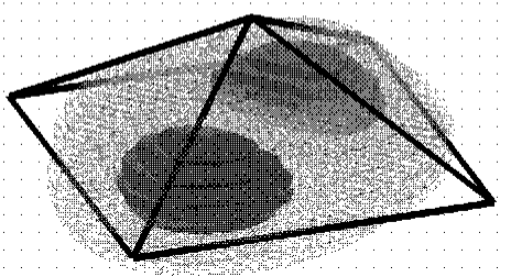
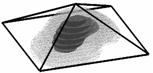
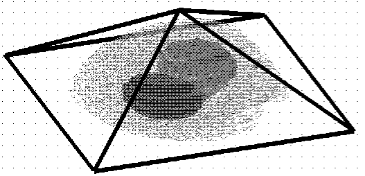
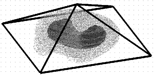
These interfacial effects also affect the one particle wave functions in the system. In Fig. 5 the isosurfaces for the squared electron wavefunctions are displayed with and without strain, respectively. The light and dark isosurface levels are selected as 0.1 and 0.5 of the maximum probability density, respectively. For both calculations, the lowest electron state is an -like state according to its nodal structure. The next two states and are -like states. These states are oriented along the and the direction, respectively. Due to the different atomic structure along these directions we find a -state splitting for the unstrained EQD of about meV. In conventional models Grundmann et al. (1995); Pryor (1998) an unstrained, square-based pyramidal EQD is modelled with a symmetry. In our microscopic model the resulting degeneracy is lifted and a splitting occurs as a consequence of the reduction of symmetry to a zinc blende symmetry.
The strain splits the states and further. Due to the
different atomic structure, the strain profile within each plane
(perpendicular to the growth z-direction) along the and
direction is different Pryor et al. (1998). This effect
contributes also to the anisotropy. Due to the fact, that the base
is larger than the top, there is a gradient in the strain tensor
between the top and the bottom of the pyramid. In the EQD, the
cation neighbors above each anion are found in direction
while the cation neighbors below are found in
-direction. Therefore, the cations along the
direction are systematically more stressed than the
cations along the direction. In case of strain we find a
-state splitting of
meV. Compared to the states and of the unstrained EQD,
the two lumps of the light isosurfaces are well separated. The
states and
reveal nodal planes along the and direction, respectively.
The state for the strained dot is resonant with a WL-state, so
the wave function is leaking into the WL. Also the wave function of
the state is localized at the base of the pyramid but clearly
shows already a finite probability density inside the WL. The states
and of the unstrained EQD are still mainly localized
inside the dot. The classification of the state by its nodal
structure is difficult. is similar to a -state which is
oriented along the direction. The electron state is
-like.
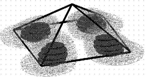
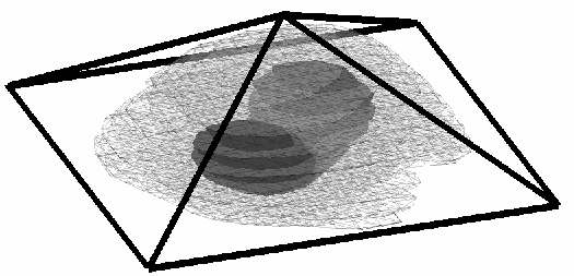
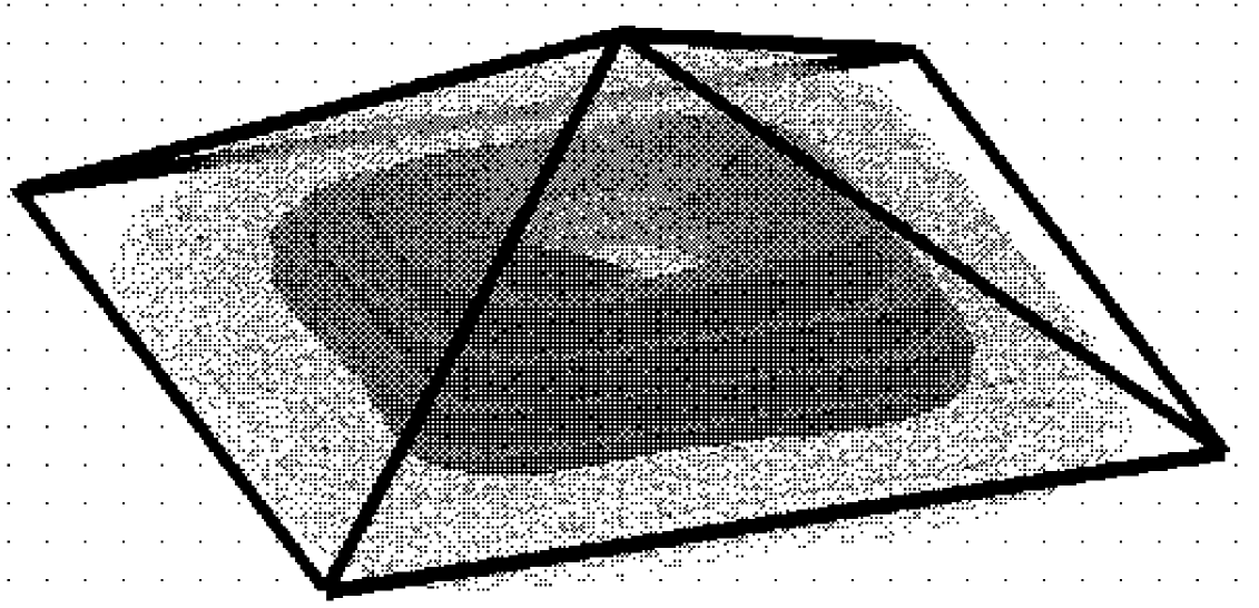
Figure 6 shows the isosurface plots of the squared wavefunction for the lowest five hole states - with and without strain. The light and dark isosurface levels are again selected as 0.1 and 0.5 of the maximum probability density, respectively. Our atomistic calculation shows that the hole states cannot be classified by -like (), -like ( and ) or -like () shape according to their nodal structures. With and without strain the hole states underly a strong band mixing. So the calculated hole states show no nodal structures. Therefore the assumption of a single heavy-hole valence-band for the description of the bound hole states in a EQD even qualitatively yields incorrect results. In contrast to quantum well systems, the light-hole and heavy-hole bands are strongly mixed in a EQD. This result is in good agreement with other multiband approaches Stier et al. (1998); Fonoberov and Baladin (2003); Pryor (1998); Wang et al. (1999, 2000); Williamson et al. (2000); Kim et al. (1998).
From Fig. 6 we can also estimate the influence of strain on the different hole states. Without strain the states and are only slightly elongated along the and direction, respectively. Due to strain these states are clearly elongated along these directions. The states - are only slightly affected by strain.
Another interesting result is that strain effects shift the electron states to lower energies and the hole states to higher energies as displayed in Fig. 4. Figure 4 also reveals that the WL ground-state for electrons and holes is shifted in a similar way due to strain. We observe that strain decreases the EQD gap by about 1.4%, lowering it from the strain-unaffected value 2.12 eV to the value 2.09 eV. For a biaxial compressive strain in a zinc blende structure, the conduction-band minimum of a bulk material is shifted to higher energies while the energy shift of the valence-band maximum depends on the magnitude of the hydrostatic and shear deformation energies Chuang (1995). So one would expect that the electron states are shifted to higher energies due to the fact that CdSe is compressively strained in the ZnSe-Matrix. This is in contradiction to the behavior we observe here. To investigate the influence of the WL states on the one-particle spectrum we use the same model geometry as shown in Fig. 2 but with a considerably smaller WL thickness of only one monolayer (ML). A 1 ML thick WL was also used before by Santoprete et al. Santoprete et al. (2003), Stier et al. Stier et al. (1998) and Wang et al. Wang et al. (1999) for an InAs/GaAs EQD. Figure 7 shows the comparison of the results for a strain-unaffected and a strained pyramidal CdSe EQD with a 1 ML thick WL and a base length of .
On the left-hand side of Fig. 7 the first five
electron and hole-state energies for an unstrained EQD are displayed
while the right-hand side shows the energies for the strained EQD.
For a 1 ML thick WL the lowest electron state is, by strain effects,
shifted to higher energies. This is what one would expect for
biaxial compression of the bulk material. Furthermore the splitting
of the -like states and is larger compared to the
results for a thick WL. The splitting of
the unstrained EQD with a thick WL is
meV whereas for the system with a 1 ML
thick WL one has meV. So the
spltting is increased by about 16 %. With
strain-effects, the splitting for the system with 1 ML WL thickness
meV is about 54 % larger
than the splitting in the system with WL thickness
meV. Also the energy
splitting between the ground state and the
first excited state is strongly influenced by the WL
thickness, namely meV for the unstrained
sytem with WL but meV for a 1
ML WL; with strain effects the splitting is
increased by about 27 % if the WL thickness is decreased from
to 1 ML. The results are summerized in
Table 3. This effect mainly arises from the fact,
that the bound states inside the dot are also coupled to the
WL-states. For a WL the wave functions of the bound states
show also a probability density inside the WL. For a thinner WL the
leaking of the states into the region of the WL is much less
pronounced. In this case, the microscopic structure inside the EQD
and also the strain-affect are much more important. This explains
the larger energy splittings in case of the 1 ML WL compared to the
results for a WL. The hole states are influenced in a
similar manner. In case of a 1 ML WL the energy spectrum of the hole
states is shifted to higher energies due to the strain-effects. This
behavior is similar to the behavior obtained from the calculations
for a WL (Fig. 7). In the 1 ML WL system the
energy splittings and for the
first three hole-states are larger than the values we obtain for the
system with WL. These splittings are also summarized in
Table 3. The WL thickness also influences the EQD
energy gap . For a 1 ML WL the
electron-states are shifted to higher energies in contrast to the
behavior of the hole states (compare Figs. 4
and 7). In case of the 1 ML WL the gap energy
is only slightly affected by the strain.
We observe here that the strain has opposite effect for electrons
and hole states: electron states become shallower, approaching the
conduction-band edge, while the hole states become deeper, moving
away from the valence-band edge.
The knowledge of the single-particle wave functions makes the
examination of many-particle effects in EQDs possible. The single
particle wave functions can be used for the calculation of Coulomb-
and dipole- matrix elements as input parameters. For example the
investigation of multi-exciton emission spectra Baer et al. (2004),
carrier capture and relaxation in semiconductor quantum dot
lasers Nielsen et al. (2004) or a quantum kinetic description of
carrier-phonon interactions Seebeck et al. (2005) is possible.
| WL | 1a | 1 ML | ||
|---|---|---|---|---|
| No Strain | Strain | No Strain | Strain | |
| [meV] | 162.8 | 161.5 | 204.1 | 221.2 |
| [meV] | 0.43 | 7.1 | 0.5 | 10.9 |
| [meV] | 5.76 | 3.7 | 7.25 | 7.66 |
| [meV] | 16.36 | 12.3 | 19.66 | 15.11 |
| [eV] | 2.12 | 2.09 | 2.21 | 2.21 |
IV Results for Nanocrystals
IV.1 Geometry and Strain
In this section we investigate the single particle states of CdSe nanocrystals within our TB-model. These nanostructures are chemically synthesized Kim et al. (2001); Guzelian et al. (1996). The nanocrystals are nearly spherical in shape Banin et al. (1999); Guzelian et al. (1996); Alivisatos (1996) and the surface is passivated by organic ligands. Due to the flexible surrounding matrix, these nanostructures are nearly unstrained Alivisatos (1996). The size of these nanostructrues is in between 10 and 40 Å in radius Banin et al. (1998, 1999); Alperson et al. (1999); Kim et al. (2001).
We model such a chemically synthesized NC as an unstrained, spherical crystallite with perfect surface passivation. The zincblende structure is assumed for the CdSe nanocrystal. We neglect surface reconstructions Pokrant and Whaley (1999); Puzder et al. (2003); Deglmann et al. (2002) and that the surface coverage with ligands is often not perfect Taylor et al. (2002), though these effects can be important especially for very small NCs. However, we concentrate on considerably larger NCs than in the before mentioned referenceses. Therefore, unlike previous TB work we concentrate here on size and the size dependence of the results obtained for the electronic structure of the NCs. The TB-parameters, which describe the coupling between the dot material and the ligand molecules, are chosen to be zero. This corresponds to an infinite potential barrier at the surface and is commonly used because of the larger band gap of the surrounding material Lippens and Lannoo (1989). An alternative approach to treat the ligand molecules is discussed by Sapra et al. in Ref. Sapra and Sarma, 2004. The influence of the organic ligands on the electronic structure can also be investigated more realistically in the framework of microscopic descriptions Pokrant and Whaley (1999); Rabani (2003); Puzder et al. (2003).
IV.2 Single particle states and comparsion with experimental results
| Electron and holes states for the nanocrystal | ||||
| Electron states | ||||
|
|
|
|

|
| Hole states | ||||
|
|
|
|

|
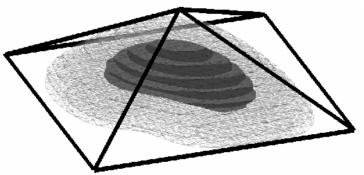
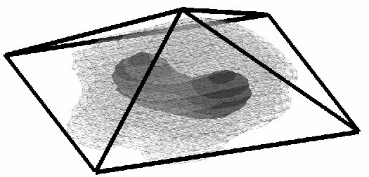
We have performed TB-calculations for finite, spherical, unstrained NCs of diameter between 1.82 nm and 4.85 nm (corresponding to 3-8 , when Å is the CdSe lattice constant of the conventional unit cell). The finite matrix diagonalizations yield both, the discrete eigenenergies and the eigenstates. For the largest NCs (of diameter 4.85 nm) results for the five lowest lying electron and hole eigenstates are shown in Fig. 8 again in the form of an isosurface plot. The lowest lying electronic state obviously has spherical symmetry and can be classified as a -state. Correspondingly the second state has the form of a -state and the states are -states and is a -like state. Despite the spherical symmetry of the system this simple classification is no longer possible for the hole states, however. Even the lowest lying hole state has no full rotational invariance, i.e. strictly speaking it cannot be classified as being an -state. This is due to the intermixing of different atomic TB-valence electron states in the NC. Similarly the higher hole states cannot clearly be classified as an - or -like state. This is an effect, which simple effective mass models cannot account for, but which will have implications in the calculation of matrix elements between these states, which enter selection rules for optical transitions etc.
In the case of an ideal zinc blende structure as considered here we do not obtain any indications of quasi-metallic behavior, i.e. of a non-vanishing (quasi continuous) spectrum of states at the Fermi energy in contrast to previous work (assuming an ideal wurtzite structure for CdSe nanocrystals) Puzder et al. (2004); Leung and Whaley (1999); Pokrant and Whaley (1999). This is probably due to the fact that this quasi-metallic behavior is due to surface states in the case when no passivation and surface reconstruction is taken into account. These surface states are formed by the dangling bonds of unsaturated Se at the NC surface, which cause -states in the band gap region Leung and Whaley (1999). In our simplified and restricted TB -basis set these -orbitals at the anions (Se) are not taken into account. Therefore, these surface states, which in reality and in more realistic models are removed (i.e. energetically drawn down and filled) due to passivation and surface reconstruction, do not occur.
The discrete electronic states of semiconductor NCs are experimentally accessible by scanning tunneling microscopy (STM) Banin et al. (1999); Alperson et al. (1999); Banin et al. (1998). The tunnel current between the metallic tip of the STM and the CdSe nanocrystal, which is e.g. epitaxially electrodeposited onto a template-stripped gold film, is measured as a function of the bias voltage . The conductance () is related to the local tunneling density of states. In the versus diagram, several discrete peaks can be observed. These peaks correspond to the addition energies (charging energies) of holes and electrons. The spacing between the various peaks can be attributed to the Coulomb charging (addition spectrum) and/or charge transfer into higher energy levels (excitation spectrum). From these measurements the energy gap as well as the splitting between electron ground state and the first excited state can be determined.
Alperson et al. Alperson et al. (1999) investigated CdSe nanocrystals with an STM. Here we compare our calculated energy gap , which is given by the difference between the electron, , and hole, , groundstate, with measured data from Ref. Alperson et al., 1999. Figure 9 displays the results for CdSe NCs with diameters in between nm and nm. Alperson et al. Alperson et al. (1999) compare the STM results (dashed dotted line) with optical spectroscopy measurements (dotted line) from Ekimov et al. Ekimov et al. (1993). The overall agreement with the TB results is very good, especially for the larger NCs. Deviations in the case of the small 2 nm NC arise from surface reconstructions Puzder et al. (2004); Deglmann et al. (2002); Pokrant and Whaley (1999) which are neglected here. When the same calculation is done without spin-orbit coupling (TB-NO SO), the energy gap is always strongly overestimated by the TB-model, in particular for smaller nanocrystals. So the spin-orbit coupling is important for a satisfactory reproduction of the experimental results. For the calculations without spin-orbit coupling, the TB-parameters are re-optimized to reproduce the characteristic properties (band gap, effective masses) of the bulk material. The re-optimized parameters are given in Table 2.
Taking into account the electron spin, the lowest electron state is twofold degenerated and -like. This
is consistent with the experimentally observed doublet Alperson et al. (1999) in the characteristic.
The next excited level is (quasi) sixfold degenerated. The spin-orbit coupling splits
this into one twofold and one fourfold degenerate state Niquet et al. (2001).
In the STM measurement Alperson et al. Alperson et al. (1999) observed such a higher multiplicity
of the second group of peaks.
This behavior has also experimentally Banin et al. (1999) and theoretically Niquet et al. (2001)
been observed for
InAs nanocrystals. The electron energy spectrum
for NCs of different diameter is shown in Fig. 10 (a). Here the first five
electron states are displayed. Note that every state is twofold degenerated due to the spin.
For the hole states the situation is more complicated.
Alperson et al. Alperson et al. (1999) observed a high density
of states at negative bias. The distinction between addition and
excitation peaks is difficult, due to the large number of
possibilities and the close proximity between the charging energy
and the level spacing. For the holes we obtain that the first two
states and are fourfold degenerated. The
energy splitting of these states is also very small. These results
are consistent to the observations of Alperson et
al. Alperson et al. (1999). Figure 10 (b) shows the
hole energy versus diamater for the spherical CdSe NCs.
Obviously, for all diameters displayed the states are
almost degenerate, i.e. including spin there is almost an 8-fold
degeneracy
of these states.
Furthermore the calculated splitting between the first two electron states and is compared with experimentally observed results for this quantity. Figure 11 shows as a function of the nanocrystal diameter . The influence of the spin-orbit coupling on our results is also investigated. We have done the calculations without (TB-NO SO) and with spin orbit-coupling (TB). The results of our TB-model for the splitting are compared with results obtained by STM Alperson et al. (1999) and by optical methods (optical) Ekimov et al. (1993). This splitting was independently determined experimentally by Guyot-Sionnest and Hines Guyot-Sionnest and Hines (1998) using infrared spectroscopy (IR). Without spin-orbit coupling the TB-model always overestimates the splitting . Especially for smaller nanocrystals the spin-orbit coupling is very important to describe the electronic structure. With spin-orbit coupling the results of the TB-model show good agreement with the experimentally observed results.
V Conclusion
We have applied an empirical TB-model to the calculation of the electronic properties of II-VI semiconductor EQDs and NCs. Assuming a zinc blende lattice and (per spin direction) one -like orbital at the cation sites and three -orbitals at the anion sites, the TB-parameters for different materials (here ZnSe and CdSe) are determined so that the most essential properties (band gap, effective masses etc.) of the known band structure of the (3 dimensional) bulk materials are well reproduced by the TB band structure. Then a CdSe QD (on top of a two-dimensional, a few atomic layers thick WL) embedded within a ZnSe matrix is modelled by using the TB-parameters of the dot material for those sites occupied by CdSe and the ZnSe TB matrix elements for the remaining sites; suitable averages have to be chosen for intersite matrix elements over and for on-site matrix elements on anion (Se) sites at interfaces between QD and barrier material. Spherical CdSe NCs can be modelled similarly by setting the intersite matrix elements between surface atoms and atoms in the monolayer of surfactant material to zero. The effects of the spin-orbit interaction, the band offsets and for the EQDs strain effects are taken into account.
For the EQD systems the numerical diagonalization yields a discrete spectrum of bound electron and hole states localized in the region of the EQD. Energetically these discrete states are below the continuum of the WL states. We have investigated the dependence on the EQD size and find that the number of the bound states and their binding energy increases with increasing dot size, therefore the effective band gap decreases. We have also investigated the dependence of the bound eigenenergies and their degeneracy on strain and on the thickness of the WL. Looking at the states themselves one sees that conduction band (electron) states can be roughly classified as -like, -like, etc. states but the valence band (hole) states cannot be classified according to such simple (,,) symmetries because they are determined by a mixing between the different (anion) -states. This cannot be accounted for by simple effective mass models but it will be important for instance for the calculation of dipole matrix elements between electron and hole states which determine the selection rules for optical transitions. For the NCs the whole spectrum is discrete, but in spite of the spherical symmetry the hole states do not have the simple ,,-symmetry but are intermixtures of atomic -orbitals. Even the lowest hole state has no spherical -symmetry but it is 4-fold (8-fold including spin) degenerate. The spin-orbit interaction is very important. Including the spin-orbit interaction we obtained nearly perfect agreement with experimental results obtained by STM for the dependence of the band gap and of the splitting of the lowest electronic states on the diameter of the NC.
Compared to (two-band) effective mass Wojs et al. (1996); Grundmann et al. (1995) and multi-band -models Stier et al. (1998); Fonoberov and Baladin (2003); Pryor (1998) for EQDs our TB model clearly has the advantage of a microscopic, atomistic description. Different atoms and constituents of the nanostructure and their actual positions are considered, and this may lead to a reduction of symmetries (for instance the symmetry instead of a -symmetry). This may automatically lift certain degeneracies and lead automatically to a splitting, for instance between and states, whereas an 8-Band- model still yields degenerate and states Pryor (1998). The effects of inhomogeneous strain can be easily incorporated into a TB model by considering the deviations of the actual atomic positions from the ideal position in the bulk crystal. Only the (empirical) pseudopotential treatmentWang et al. (1999, 2000); Williamson et al. (2000); Kim et al. (1998) may be still superior and more accurate than the TB approach, but in a pseudopotential descripion a variation of the wave functions within the individual atoms is accounted for and a large number of basis states is required. Therefore, a TB description is simpler and quicker and allows for the investigation of larger nanostructures without loosing information on the essential, microscopic details of the structure. Compared to other TB models of QD structures, we do not consider free standing, isolated QDs (as in Ref. Saito et al., 1998) but we can describe realistic QDs (with a WL) embedded into another barrier material. We show here that a reduced -basis is already sufficient for a satisfying reproduction of properties like optical gaps, energy splittings, etc., and their size dependence. Much larger basis sets, namely a -basisSantoprete et al. (2003) or even a -basisJancu et al. (1998) were used in previous TB-models of EQDs. Our reduced, smaller basis set, of course, leads to computational simplifications and allows for the treatment of larger QDs. Furthermore, we apply our TB-model to different materials than investigated previously, namely II-VI CdSe nanostructures, and we investigate also NCs, for which excellent agreement with experimental STM-results could be demonstrated.
In the future further applications of our TB-model for embedded semiconductor QDs and NCs are planned. Of course applications to QDs of other materials, for instance nitride systems, and other (e.g. wurtzite) crystal structures are possible. Furthermore, EQDs of other shape and size (dome-shaped, lens-shaped, truncated cones, etc.) or two coupled QDs or freestanding (capped and uncapped) QDs can be investigated. A combination with ab-initio calculations is also possible by determining the TB-parameters from a first-principles band structure calculation of the bulk material. Furthermore the influence of surface reconstructions and the surfactant material on the results for NCs should be investigated. Especially for small NCs these effects are important. Finally matrix elements of certain observables like dipole matrix elements between the calculated QD electron and hole states can be determined, which are important for selection rules and the optical properties of these systems.
Acknowledgements.
This work has been supported by a grant from the Deutsche Forschungsgemeinschaft No. Cz-31/14-1,2 and by a grant for CPU time from the John von Neumann Institute for Computing at the Forschungszentrum Jülich.References
- Woggon (1997) U. Woggon, Optical properties of semiconductor quantum dots (Springer, Berlin, 1997).
- Michler (2000) P. Michler, Single Quantum Dots: Fundamentals, Applications, and New Concepts (Topics in Applied Physics) (Springer, Berlin, 2000).
- Passaseo et al. (2001) A. Passaseo, R. Rinaldi, M. Longo, S. Antonaci, A. L. Convertino, R. Cingolani, A. Taurino, and M. Catalano, J. Appl. Phys. 89 (2001).
- Grundmann (2002) M. Grundmann, Nano-Optoelectronics: Concepts, Physics and Devices (Springer, Berlin, 2002).
- Michler et al. (2000) P. Michler, A. Kiraz, C. Becher, W. V. Schoenfeld, P. M. Petroff, L. Zhang, E. Hu, and A. Imamoglu, Science 290, 2282 (2000).
- Li et al. (2003) X. Li, Y. Wu, D. Steel, D. Gammon, T. H. Stievater, D. S. Katzer, D. Park, C. Piermarocchi, and L. J. Sham, Science 301, 809 (2003).
- van der Wiel et al. (2003) W. G. van der Wiel, S. D. Franceschi, J. M. Elzerman, T. Fujisawa, S. Tarucha, and L. P. Kouwenhoven, Rev. Mod. Phys. 75, 1 (2003).
- Merz et al. (1998) J. L. Merz, S. Lee, and J. K. Furdyna, Journal of Crystal Growth 184, 228 (1998).
- Yang et al. (2001) Y. Yang, D. Z. Shen, J. Y. Zhang, X. W. Fan, B. S. Li, Y. M. Lu, Y. C. Liu, and Y. N. Liu, Journal of Crystal Growth 233, 785 (2001).
- Zhang et al. (2001) B. P. Zhang, D. D. Manh, K. Wakatsuki, and Y. Segawa, Journal of Crystal Growth 227, 645 (2001).
- Kim et al. (2001) B. S. Kim, M. A. Islam, L. E. Brus, and I. P. Herman, J. Appl. Phys. 89, 8127 (2001).
- Guzelian et al. (1996) A. A. Guzelian, U. Banin, A. V. Kadavanich, X. Peng, and A. P. Alivisatos, Appl. Phys. Lett. 69, 1432 (1996).
- Manna et al. (2000) L. Manna, E. C. Scher, and A. P. Alivisatos, J. Am. Chem. Soc. 122, 12700 (2000).
- Murray et al. (2001) C. B. Murray, S. Sun, W. Gaschler, H. Doyle, T. A. Betley, and C. R. Kagan, IBM J. Res. & Dev. 45, 47 (2001).
- Wojs et al. (1996) A. Wojs, P. Hawrylak, S. Fafard, and L. Jacak, Phys. Rev. B 54, 5604 (1996).
- Fry et al. (2000) P. W. Fry, I. E. Itskevich, D. J. Mowbray, M. S. Skolnick, J. J. Finley, J. A. Barker, E. P. O’Reilly, L. R. Wilson, I. A. Larkin, P. A. Maksym, et al., Phys. Rev. Lett. 84, 733 (2000).
- Ruvimov et al. (1995) S. Ruvimov, P. Werner, K. Scheerschmidt, U. Gösele, J. Heydenreich, U. Richter, N. N. Ledentsov, M. Grundmann, D. Bimberg, V. M. Ustinov, et al., Phys. Rev. B 51, R14766 (1995).
- Shumway et al. (2001) J. Shumway, A. J. Williamson, A. Zunger, A. Passaseo, M. DeGiorgi, R. Cingolani, M. Catalano, and P. Crozier, Phys. Rev. B 64, 125302 (2001).
- Puzder et al. (2004) A. Puzder, A. J. Williamson, F. Gygi, and G. Galli, Phys. Rev. Lett. 92, 217401 (2004).
- Sarkar and Springborg (2003) P. Sarkar and M. Springborg, Phys. Rev. B 68, 235409 (2003).
- Deglmann et al. (2002) P. Deglmann, R. Ahlrichs, and K. Tsereteli, J. Chem. Phys. 116, 1585 (2002).
- Grundmann et al. (1995) M. Grundmann, O. Stier, and D. Bimberg, Phys. Rev. B 52, 11969 (1995).
- Stier et al. (1998) O. Stier, M. Grundmann, and D. Bimberg, Phys. Rev. B 59, 5688 (1998).
- Fonoberov and Baladin (2003) V. A. Fonoberov and A. A. Baladin, J. Appl. Phys. 94, 7178 (2003).
- Pryor (1998) C. Pryor, Phys. Rev. B 57, 7190 (1998).
- Wang et al. (1999) L.-W. Wang, J. Kim, and A. Zunger, Phys. Rev. B 59, 5678 (1999).
- Wang et al. (2000) L. W. Wang, A. J. Williamson, A. Zunger, H. Jiang, and J. Singh, Appl. Phys. Lett. 76, 339 (2000).
- Williamson et al. (2000) A. J. Williamson, L. W. Wang, and A. Zunger, Phys. Rev. B 62, 12963 (2000).
- Kim et al. (1998) J. Kim, L. W. Wang, and A. Zunger, Phys. Rev. B 57, R9408 (1998).
- Saito and Arakawa (2002) T. Saito and Y. Arakawa, Physica E 15, 169 (2002).
- Lee et al. (2001) S. Lee, L. Jönsson, J. W. Wilkins, G. W. Bryant, and G. Klimeck, Phys. Rev. B 63, 195318 (2001).
- Lee et al. (2002) S. Lee, J. Kim, L. Jönsson, J. W. Wilkins, G. W. Bryant, and G. Klimeck, Phys. Rev. B 66, 235307 (2002).
- Allan et al. (2000) G. Allan, Y. M. Niquet, and C. Delerue, Appl. Phys. Lett. 77, 639 (2000).
- Niquet et al. (2001) Y. M. Niquet, C. Delerue, M. Lannoo, and G. Allan, Phys. Rev. B 64, 113305 (2001).
- Santoprete et al. (2003) R. Santoprete, B. Koiller, R. B. Capaz, P. Kratzer, Q. K. K. Liu, and M. Scheffler, Phys. Rev. B 68, 235311 (2003).
- Hill and Whaley (1994) N. A. Hill and K. B. Whaley, J. Chem. Phys. 100, 2831 (1994).
- Leung et al. (1998) K. Leung, S. Pokrant, and K. B. Whaley, Phys. Rev. B 57, 12291 (1998).
- Leung and Whaley (1999) K. Leung and K. B. Whaley, J. Chem. Phys. 100, 11012 (1999).
- Pokrant and Whaley (1999) S. Pokrant and K. B. Whaley, Eur. Phys. J. D 6, 255 (1999).
- Schrier and Whaley (2003) J. Schrier and K. B. Whaley, Phys. Rev. B 67, 235301 (2003).
- Lee et al. (2004) S. Lee, O. L. Lazarenkova, P. von Allmen, F. Oyafuso, and G. Klimeck, Phys. Rev. B 70, 125307 (2004).
- Saito et al. (1998) T. Saito, J. N. Schulman, and Y. Arakawa, Phys. Rev. B 57, 13016 (1998).
- Kim et al. (1994) Y. D. Kim, M. V. Klein, S. F. Ren, Y. C. Chang, H. Luo, N. Samarth, and J. K. Furdyna, Phys. Rev. B 49, 7262 (1994).
- Hölscher et al. (1985) H. W. Hölscher, A. Nöthe, and C. Uihlein, Phys. Rev. B 31, 2379 (1985).
- Pellegrini et al. (1995) V. Pellegrini, R. Atanasov, A. Tredicucci, F. Beltram, C. Amzulini, L. Sorba, L. Vanzetti, and A. Franciosi, Phys. Rev. B 51, 5171 (1995).
- Dierks and Czycholl (1998) H. Dierks and G. Czycholl, Journal of Crystal Growth 185, 877 (1998).
- Chadi (1977) D. J. Chadi, Phys. Rev. B 16, 790 (1977).
- Slater and Koster (1954) J. C. Slater and G. F. Koster, Phys. Rev. 94, 1498 (1954).
- Cohen and Chelikowski (1989) M. L. Cohen and J. R. Chelikowski, Electronic Structure and Optical Properties of Semiconductors (Springer Series in Solid-State Sciences 75, Second Edition, Berlin, 1989).
- Rabani (2003) E. Rabani, J. Chem. Phys. 115, 2361 (2003).
- Puzder et al. (2003) A. Puzder, A. J. Williams, N. Zaitseva, G. Galli, L. Manna, and A. Alivisatos, Nanoletters 4, 2361 (2003).
- Kurtz et al. (2001) E. Kurtz, M. Schmidt, M. Baldauf, S. Wachter, M. Grün, H. Kalt, and C. Klingshirn, Appl. Phys. Lett. 79, 1118 (2001).
- Lakes et al. (1996) S. Lakes, T. Reisinger, B. Hahn, C. Meier, M. Meier, and W. Gebhardt, Journal of Crystal Growth 159, 480 (1996).
- Froyen and Harrison (1979) S. Froyen and W. A. Harrison, Phys. Rev. B 20, 2420 (1979).
- Sapra et al. (2002) S. Sapra, N. Shanthi, and D. D. Sarma, Phys. Rev. B 66, 205202 (2002).
- Jancu et al. (1998) J. M. Jancu, R. Scholz, F. Beltram, and F. Bassani, Phys. Rev. B 57, 6493 (1998).
- Bertho et al. (1991) D. Bertho, D. Boiron, A. Simon, C. Jouanin, and C. Priester, Phys. Rev. B 44, 6118 (1991).
- Wang and Zunger (1994) L.-W. Wang and A. Zunger, J. Chem. Phys. 100, 2394 (1994).
- Chuang (1995) S. L. Chuang, Physics of Optoelectronic Devices (Wiley-Interscience Plublication, New York, 1995).
- Pryor et al. (1998) C. Pryor, J. Kim, L. W. Wang, A. J. Williamson, and A. Zunger, Appl. Phys. Lett. 72, 2011 (1998).
- Baer et al. (2004) N. Baer, P. Gartner, and F. Jahnke, Eur. Phys. J. B 42, 231 (2004).
- Nielsen et al. (2004) T. R. Nielsen, P. Gartner, and F. Jahnke, Phys. Rev. B 69, 235314 (2004).
- Seebeck et al. (2005) J. Seebeck, T. R. Nielsen, P. Gartner, and F. Jahnke, Phys. Rev. B 71, 125327 (2005).
- Banin et al. (1999) U. Banin, C. YunWei, D. Katz, and O. Millo, Nature 400, 542 (1999).
- Alivisatos (1996) A. P. Alivisatos, Science 271, 933 (1996).
- Banin et al. (1998) U. Banin, C. J. Lee, A. A. Guzelian, A. V. Kadavanich, A. P. Alivisatos, W. Jaskolski, G. W. Bryant, A. L. Efros, and M. Rosen, J. Chem. Phys. 109, 2306 (1998).
- Alperson et al. (1999) B. Alperson, I. Rubinstein, G. Hodes, D. Porath, and O. Millo, Appl. Phys. Lett. 75, 1751 (1999).
- Taylor et al. (2002) J. Taylor, T. Kippeny, and S. J. Rosenthal, J. Cluster Sci. 12, 571 (2002).
- Lippens and Lannoo (1989) P. E. Lippens and M. Lannoo, Phys. Rev. B 39, 10935 (1989).
- Sapra and Sarma (2004) S. Sapra and D. D. Sarma, Phys. Rev. B 69, 125304 (2004).
- Ekimov et al. (1993) A. I. Ekimov, F.Hache, M. C. Schanne-Klein, D. Ricard, C. Flytzanis, I. A. Kudryavtsev, T. V. Yazeva, A. V. Rodina, and A. L. Efros, J. Opt. Soc. Am. B 10, 100 (1993).
- Guyot-Sionnest and Hines (1998) P. Guyot-Sionnest and M. A. Hines, Appl. Phys. Lett. 72, 686 (1998).