Distribution of conduction channels in nanoscale contacts: evolution towards the diffusive limit
Abstract
We present an experimental determination of the conduction channel distribution in lead nanoscale contacts with total conductances ranging from 1 to 15 , where . It is found that even for contacts having a cross section much smaller than the mean free path the distribution tends to be remarkably close to the universal diffusive limit. With the help of theoretical calculations we show that this behavior can be associated with the specific band structure of lead which produces a significant contribution of partially open channels even in the absence of atomic disorder. Published in Europhysics Letters, http://www.edpsciences.org/articles/epl/abs/2005/11/epl8748/epl8748.html.
pacs:
73.23.-b, 73.63.Rt, 73.40.JnElectron transport properties in a quantum coherent conductor are fully characterized by the set of transmission coefficients corresponding to the conductance eigenchannels of the system landauer ; buttiker . Clearly, the whole set cannot be extracted from the total conductance which only yields information on . The possibility of an accurate determination of the individual was demonstrated by Scheer et al. Scheer98 for the case of one-atom contacts, by analyzing electron transport in the superconducting state Naveh . This technique allowed to prove that the number of channels for one-atom contacts is basically determined by the valence orbital structure while the particular values in the set depend also on the contact geometry at the atomic scale review .
A natural question that arises is how the set evolves as the size of the contact is increased. One would expect that for sufficiently large contacts (where the size is larger than the mean free path) the transmission coefficients would be distributed according to , i.e. the universal distribution function predicted for a quantum conductor in the diffusive regime dorokhov82 ; Beenakker97 . Although indirect evidence of this distribution has been obtained through shot-noise measurements shotnoise a direct determination of in this regime is still an open experimental challenge.
In the present work we combine experimental and theoretical efforts in order to analyze the evolution of the channel distribution in nanocontacts as the size of the contact is increased from the atomic-size limit. We obtain the set from transport measurements in lead nanocontacts with conductances ranging from 1 to 15 . These results are compared with model calculations in which the effects of geometry, atomic disorder, and band structure can be included. We find that even for small contacts (3–4 ) the channels distribution for Pb is unexpectedly close to the diffusive limit. We show that this behavior can be attributed to the particular band structure of Pb.
Highly stable atomic scale contacts are formed using a mechanically controlled break-junction (MCBJ) muller . A notched lead wire 99.99% pure is glued on top of a flexible substrate. The rupture of the wire is carried out at 1.6 K in He exchange gas, thus preventing the freshly exposed surfaces from oxidizing. The contact can be reestablished and broken with picometer displacement resolution and stability.
It was shown that in one-atom contacts the can be obtained from the experimental current-voltage characteristic curve (IV) by fitting to the sum of one-channel IV curves, Scheer97 ; Scheer98 , which have been calculated elsewhere for arbitrary transmission subgap .
Scheer et al. Scheer97 ; Scheer98 determined the transmission of a small number of channels for one-atom contacts using a steepest descent based method privatecomm. . For larger contacts we have found that a simulated annealing algorithm is much more efficient. It is faster, a fact that becomes increasingly important as the number of channels to fit grows, and has the advantage of avoiding getting trapped at local minima. We use as acceptance criterion the root mean square deviation from the measured IV curve, . The fit starts from a random initial position in the -dimensional space spanned by . Then a random walk is performed. At each step the new fit is accepted if is smaller than the previous one. If is larger the step can still be accepted, according to a Boltzmann-type factor, with a pseudo-temperature which is lowered in a smooth way. is chosen large enough for the fit to result in several closed channels ().
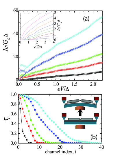
We show in fig. 1 a) IV curves for different contact realizations. These IV curves exhibit subharmonic gap structure for voltages below due to multiple Andreev reflections subgap . At low voltages the IV curves show a contribution from the supercurrent peak and is not taken into account.
In fig. 1 b) we show the channel transmissions obtained from the fit to the IV curves in fig. 1 a). Channel indexes are ordered in decreasing transmission. An estimate of can be obtained from a finite number of experimental realizations in the following way. A histogram of the values is constructed dividing the transmission axis into 14 equally sized bins. The values falling within the range of each bin are collected from 20 contact realizations of a given conductance. The result is normalized dividing by the conductance times the number of realizations. We find that is bimodal, with a significant number of channels with high transmission.
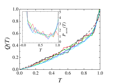
The channel distribution can be also conveniently presented using the well-behaved integrated quantity schep-bauer :
| (1) |
which is a regular function of . is the relative contribution to the conductance of all channels with .
We obtain an estimate of from 20 experimental realizations making a histogram with a bin size equal to 0.01. The values that are lower than from all realizations of a given conductance are collected and added. Then the result is normalized dividing by . For a perfect ballistic conductor this function is zero except for . The distribution shown in fig. 2 is not very sensitive to the size of the contact and remarkably similar to the universal diffusive limit. This similarity is rather unexpected due to the small size of the contact with less than 20 atoms in cross section.
Previous experience for the case of one-atom contacts has demonstrated that band structure effects play a major role in the determination of the set for a given element us98 ; Scheer98 ; byge1 ; mingo ; byge2 . It is thus interesting to analyze whether this is still the case for contacts in the intermediate range (larger than one atom but smaller than the mean free path). For this purpose we have performed model calculations of the set for idealized geometries of the nanocontacts.
As in previous studies we use a self-consistent parametrized tight-binding (TB) model in which the main features of the bulk band-structure are included us98 . We shall consider model geometries like the ones depicted in the insets of fig. 3 in which the neck of the contact is represented by several atomic layers of different cross section grown along the (111) direction on a fcc lattice. This central region is connected to the left and right electrodes represented by perfect semi-infinite crystals. The corresponding TB Hamiltonian can be written as + + + , where and describe the uncoupled left and right electrodes and the central part of the contact respectively; being a coupling term between the central region and the electrodes. The matrix elements , where and design sites and orbitals respectively, are taken from fits to the bulk ab-initio band structure. As a self-consistency condition we impose local charge neutrality on each site. Disorder in the atomic positions at the central region can be included by rescaling the hopping elements according to the distortion of the different bond length with respect to the bulk values comment-hopping .
Once the TB Hamiltonian has been built the conductance = is calculated in terms of the matrix elements of the Green function operator = using :
| (2) |
where are the matrix tunneling rates connecting the central region to the leads us98 . The transmission matrix can then be diagonalized in order to obtain the transmission eigenchannels and eigenvalues .
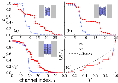
In fig. 3 we show typical results for the transmission sets that are obtained for Pb contacts of intermediate cross section. The effect of an specific contact geometry is illustrated in the upper panels (fig. 3 a) and b)). As can be observed, a characteristic feature of Pb is the appearance of steps corresponding to partially open channels with similar transmission. For comparison we also show in this figure the corresponding results for Au contacts in order to remark the differences with a monovalent metal. Although the detailed structure of these curves is strongly dependent on the specific geometry, the behavior for Pb is clearly in contrast to the one observed in Au where partially open channels are rarely observed. These differences can be directly related to the particular band structure of both metals. While in the case of Au the channels can be associated with a single band of s-character at the Fermi energy, in Pb the channels arise from the contribution of several bands with sp-character. In fact, for the same geometry the total number of channels with significant transmission is larger for Pb than for Au. When the cross section of the contact is increased (fig. 3 c)) the partially open channels in Pb tend to define a rather continuous distribution which fairly resembles that of a diffusive conductor. In panel d) we compare the corresponding distributions with the result expected for a diffusive wire.
As a result of these previous calculations one can conclude that, even in the absence of atomic disorder, Pb contacts deviate strongly from the ballistic behavior observed in the case of Au.
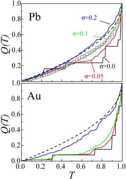
In a second step we have analyzed the influence of atomic disorder in the calculated distributions. Disorder is assumed to be localized in the neck region (we will discuss later the effect of disorder on the bulk electrodes). The degree of disorder is characterized by the mean square deviation of the bond lengths with respect to the idealized structure, . fig. 4 shows the evolution of the distribution function as is increased for a particular contact geometry. As can be observed for Pb the distribution tends rather quickly to the diffusive one with increasing disorder. We also show the experimental distribution in which several cases with total conductances ranging from 10 to 15 have been averaged. This distribution is in fairly good agreement with the calculated one for the case , which roughly corresponds to a mean free path nm. This rather low degree of disorder is consistent with what is known both from molecular-dynamics simulations and images made by transmission electron microscopy of metallic nanocontacts review .
It should be stressed that these distributions still exhibit some deviations with respect to the universal curve, specially for high transmission. We can associate these deviations with the fact that the size of the contact is still considerably smaller than the mean free path.
In contrast to the case of Pb, Au exhibits a clear deviation from the universal distribution even for the larger values of considered. Notice that already corresponds to an unexpectedly high degree of disorder comment-disorder .
As a final issue we estimate the effect of disorder on the bulk electrodes by means of a phenomenological model. In this model the electrodes are diffusive conductors characterized by a classical probability for returning to the contact region after a given time . Modelling the electrode as a cone with openning angle this probabilitiy is given by , where and are the Fermi wavevector and velocityrespectively and is the diffusive constant ludoph99 . Following the arguments of ref. ludoph99 the correction to the transmission distribution can be written as
| (3) |
where is the elastic scattering time and . Assuming that typically and that can range from nm to nm in Pb, one obtains leading to a rather small correction which hardly modifies the theoretical results already shown in fig. 4.
In conclusion, we have presented a combined experimental and theoretical analysis of the conduction channel distribution of nanoscale contacts with several atoms in cross section. The experimental method demonstrates the applicability of the technique developed by Scheer et al. Scheer97 ; Scheer98 to much larger contacts. It is found that for Pb contacts the distribution tends rather fast to the universal diffusive limit. We show that this behavior can be associated with the specific band structure of Pb which favors the appearance of partially open channels in contrast to what is predicted for monovalent metals like Au.
Acknowledgements.
We thank S. Vieira for useful comments and continuous support. This work has been financed by the MCyT under project MAT2002-11982-E within the EUROCORES Programme SONS of the European Science Foundation, which is also supported by the European Commission, Sixth Framework Programme and by MCyT (BFM2001 0150 and MAT2001 1281), GR/MAT/0111/2004 and CAM (07N/0053/2002 and 07N/0039/2002).References
- (1) R. Landauer, IBM J. Res. Dev., 1, 223 (1957).
- (2) M. Büttiker, Phys. Rev. B, 33, 3020 (1986).
- (3) E. Scheer et al., Nature 394, 154 (1998).
- (4) The case of highly conductive tunnel junctions was studied in Y. Naveh et al., Phys. Rev. Lett. 85, 5404 (2000).
- (5) For a review on atomic-sized conductors see N. Agraït, A. Levy Yeyati, and J. M. van Ruitenbeek, Phys. Rep. 377, 81(2003).
- (6) O.N. Dorokhov, JETP Lett. 36, 318 (1982).
- (7) C.W.J. Beenakker, Rev. Mod. Phys. 69, 731 (1997).
- (8) A.H. Steinbach, J.M. Martinis, and M.H. Devoret, Phys. Rev. Lett. 76, 3806 (1996); M. Henny et al., Appl. Phys. Lett. 71, 773 (1997); R. Schoelkopf et al., Phys. Rev. Lett. 78, 3370 (1997).
- (9) C.J. Muller, J.M. van Ruitenbeek, and L.J. de Jongh, Physica C 191, 485 (1992).
- (10) E. Scheer et al., Phys. Rev. Lett. 78, 3535 (1997).
- (11) D.V. Averin and A. Bardas, Phys. Rev. Lett. 75, 1831 (1995); J.C. Cuevas, A. Martín-Rodero, and A. Levy Yeyati, Phys. Rev. B 54, 7366 (1996); E.N. Bratus et al., Phys. Rev. B 55, 1266 (1997).
- (12) C. Urbina (private communication).
- (13) K.M. Schep and G.E.W. Bauer, Phys. Rev. Lett. 78, 3015 (1997).
- (14) J.C. Cuevas, A. Levy Yeyati, and A. Martín-Rodero, Phys. Rev. Lett. 80, 1066 (1998).
- (15) M. Brandbyge, M. R. Sørensen, and K. W. Jacobsen, Phys. Rev. B 56, 14956 (1997).
- (16) C. Sirvent, J. G. Rodrigo, S. Vieira, L. Jurczyszyn, N. Mingo, and F. Flores Phys. Rev. B 53, 16086 (1996).
- (17) N. Kobayashi, M. Brandbyge, and M. Tsukada, Phys. Rev. B 62, 8430 (2000).
- (18) Scaling laws for the hopping elements are discussed in D.A. Papaconstantopoulos, Handbook of the band structure of elemental solids, Plenum Press, New York (1986).
- (19) We have estimated that in Pb corresponds roughly to a mean free path nm, i.e. a much smaller value than expected for the bulk metal.
- (20) B. Ludoph et al., Phys. Rev. Lett. 82, 1530 (1999).