Ga-induced atom wire formation and passivation of stepped Si(112)
Abstract
We present an in-depth analysis of the atomic and electronic structure of the quasi one-dimensional (1D) surface reconstruction of Ga on Si(112) based on Scanning Tunneling Microscopy and Spectroscopy (STM and STS), Rutherford Backscattering Spectrometry (RBS) and Density Functional Theory (DFT) calculations. A new structural model of the Si(112)-Ga surface is inferred. It consists of Ga zig-zag chains that are intersected by quasi-periodic vacancy lines or misfit dislocations. The experimentally observed meandering of the vacancy lines is caused by the co-existence of competing and unit cells and by the orientational disorder of symmetry breaking Si-Ga dimers inside the vacancy lines. The Ga atoms are fully coordinated, and the surface is chemically passivated. STS data reveal a semiconducting surface and show excellent agreement with calculated Local Density of States (LDOS) and STS curves. The energy gain obtained by fully passivating the surface calls the idea of step-edge decoration as a viable growth method toward 1D metallic structures into question.
pacs:
68.35.-p, 68.37.Ef, 73.20.At, 81.07.VbI Introduction
Nature only provides few one-dimensional (1D) electronic systems, such as carbon nanotubes,Postma et al. (2000) organic charge transfer salts, and inorganic blue bronzes (see for example the discussion in Ref. Grioni et al., 1999). Electrons confined to one dimension are fundamentally different from the quasi-particles of Fermi liquid theory.Voit (1994) In 1D, even in the case of arbitrary low interaction strength, the single-particle description of the system breaks down and must be replaced by a description based on collective excitations.Voit (1994) Experimental realization and verification of this Luttinger liquid phenomenon continues to capture the imagination of physicists, especially since the fabrication of structurally uniform 1D nanostructures now appears to be within the realm of possibilities.
A very intuitive approach to produce 1D systems is to utilize high index silicon surfaces.Himpsel et al. (2001) Based on the concept of metal-adatom step-edge decoration, deposition of a submonolayer amount of metal atoms onto a stepped Si surface is expected to result in a single domain of quasi 1D, metallic atomic wires, i.e. an atom wire array.Himpsel et al. (2001) In contrast to for example carbon nanotubes, such a single domain surface quantum wire array would be easily accessible to both nanoscopic and macroscopic techniques such as Scanning Tunneling Microscopy and Spectroscopy (STM and STS), photoemission spectroscopy, and (surface) transport measurements. In addition, the coupling strength between the atom wires can be tuned by changing the miscut angle of the vicinal Si surface, i.e. adjusting the separation between the wires.Crain et al. (2004)
Indeed such single domain 1D metallic systems have been produced on high index Si surfaces.Crain et al. (2004); Starowicz et al. (2002); Segovia et al. (1999); Yeom et al. (1999); Ahn et al. (2004) However, the metal adatoms in these studies are generally not adsorbed at the step edges. Instead, rather complicated reconstructions are formed with chains of metal atoms that are incorporated into the (111)-like terraces in the unit cell.Bunk et al. (1999); Robinson et al. (2002); Crain et al. (2004) This questions the idea of forming atom wires via step-edge decoration on Si. Furthermore, it was noticedGonzález et al. (2004) that these 1D atomic-scale systems all exhibit intrinsic spatial disorder in the atomic structure, which will have important consequences for electronic transport in these systems. It should be noted that in the case that step-edge decoration does not occur in these studies, the miscut or vicinal orientation of the Si surfaces mainly serves to create a single domain surface reconstruction; similar or ”parent” reconstructions exist on the corresponding planar surfaces. These single domain quantum wire arrays have been studied successfully with Angle Resolved Photoelectron Spectroscopy (ARPES)Crain et al. (2003, 2004); Ahn et al. (2003, 2004); Matsuda et al. (2003) and transport measurements.Kanagawa et al. (2003)
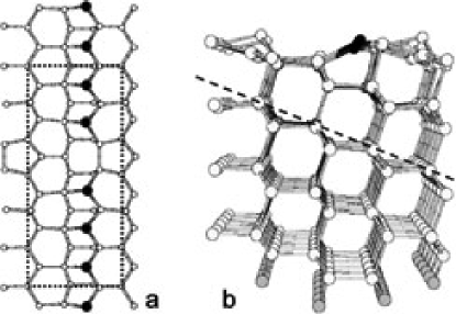
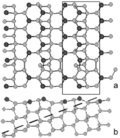
In this paper, we investigate the formation of Ga chains on the vicinal Si(112) surface. A structural model for this interface was devised by Jung, Kaplan and Prokes (the JKP-model ).Jung et al. (1993, 1994); Yater et al. (1995); Baski et al. (1999); Erwin et al. (1999); Yoo et al. (2002) The unit cell of the bulk terminated vicinal Si(112) surface contains a double-width (111)-like terrace with single (111)-like steps. Based on Low Energy Electron Diffraction (LEED) and Auger Electron Spectroscopy (AES) experiments,Jung et al. (1993, 1994); Yater et al. (1995) it was proposed that Ga atoms adsorb at the step edges of the bulk terminated unit cell, thus forming atom rows along the [10] direction. Missing Ga atoms or vacancies in these Ga rows align into quasi 1D vacancy lines that run orthogonal to the Ga rows, resulting in the observed periodicity. In this model the Ga coverage is of a Si(111) bilayer, or five atoms per unit cell.Jung et al. (1994) Later STM experiments by Baski et al.Baski and Whitman (1996); Baski et al. (1999) seemed to confirm this model. These authors observed a well-ordered array of single-atom rows with a regular row spacing 9.4 Å, equal to the step-edge spacing of bulk terminated Si(112); see for example Fig. 1 of Ref. Baski et al., 1999. A side view and a top view representation of this JKP-model is shown in Fig. 1.
As a consequence of the three-fold coordination of the adsorption sites, the trivalent Ga atoms are fully coordinated. There are no partially filled dangling bonds on the Ga atoms and the covalently bonded Ga atoms would not contribute any state density near the Fermi level. However, an interesting feature which has remained largely unnoticed in literature is the fact that within the JKP model, there should exist a metallic dangling bond wire that is located on the row of Si surface atoms located in between the Ga rows. However, the predicted 1D metallicity turned out to be unstable with respect to a Jahn-Teller distortion, leaving only one unpaired electron per unit cell. Interestingly, the resulting electronic structure implied the existence of conduction channels orthogonal to the Ga chains.Yoo et al. (2002)
We have performed a detailed Scanning Tunneling Microscopy (STM) study of the Si(112)-Ga surface. Because of the unprecedented resolution in the STM images of the Si(112)-Ga surface, a detailed investigation of the atomic structure of the Si(112)-Ga surface could be carried out. Extensive Density Functional Theory (DFT) calculations have been performed to explore new candidate structural models. Theoretical STM images were calculated for the new structures and compared with the experimental STM images. From a detailed analysis of all experimental and theoretical information, a new structural model for the Si(112)-Ga surface emerged, which shows excellent agreement with the experimental evidence. It contains two Ga atom rows amounting to a total of ten Ga atoms per unit cell, consistent with RBS experiments. The two Ga rows form zig-zag chains while quasi-periodic vacancy lines intersect these Ga chains. The observed meandering of the vacancy lines can also be fully explained within this model. STS measurements show that the surface is semiconducting, and are consistent with our band structure calculations and theoretical STS simulations. This paper presents a follow-up of an initial reportGonzález et al. (2004) with new data and provides a more detailed and in depth analysis, including a detailed comparison between spatially resolved STS and theoretical local density of states (LDOS) calculations.
II Experimental and theoretical procedures
Experiments were carried out in an ultra-high vacuum system with a base pressure 5 mbar. The system was equipped with a Ga effusion cell, direct current sample heating facilities, an Omicron variable temperature STM and a LEED system. An n-type Si(112) wafer (, orientation 2∘ of the nominal (112) orientation) was cut into (102)-mm2 samples and rinsed in acetone and isopropanol. After introduction into UHV the samples were degassed at 775 K overnight and subsequently the sample temperature was slowly raised to 1025 K and kept there for 4 hrs. Next, the sample was flashed at 1475 K to remove the native oxide. During resistive heating, the current was directed parallel to the nano-facets of the clean (112) surface (i.e. in the [10] direction) in order to avoid current-induced step bunching. The surface reconstruction was prepared in two different ways. In the ”one-step” procedure, Ga was deposited with the Si substrate held at 825 50 K.Glembocki and Proke (1997) In the ”two-step” procedure, Ga is deposited onto a Si(112) substrate kept at room temperature. After Ga deposition the sample was annealed at about 825 50 K to form the 61 reconstruction and to desorb excess Ga atoms.Baski et al. (1999) Both surface preparation procedures resulted in identical LEED patterns and STM images. The pressure remained below 2 mbar during sample preparation. The sample temperature during sample preparation was measured using an optical pyrometer. STM and STS experiments were performed at room temperature and at low temperature ( K) using etched tungsten tips. STM images of the filled and empty electronic states were obtained with a constant current between 0.05 and 0.2 nA and bias voltages between 1 and 2 V. STS data were acquired with a setpoint of 0.3 nA at 1 V.
RBS experiments were carried out at the AMOLF institute in Amsterdam to determine the amount of Ga atoms per surface unit cell. A normal incident 2.0 MeV He+ ion beam from a Van de Graaf accelerator was backscattered from the Si crystal and detected at a backscattering angle of 165∘. The beam current was typically about 20 nA.
The atomic and electronic structure of new candidate structural models for the Si(112)-Ga surface, corresponding to Ga-coverages ranging from 5 to 11 Ga atoms per 61 unit cell were explored using an efficient local-orbital (LO) DFT technique (the Fireball96 code).Demkov et al. (1995) In these calculations, we have used a minimal atomic-like basis set using the following cut-off radii () for the definition of the Fireball96 orbitals Sankey and Niklewski (1989): , . For the most promising structures, Plane-Waves (PW) DFT calculations (Castep code)CAS were also performed to check the validity of the Fireball96 findings. In these PW calculations, we have used a kinetic energy cut-off of 200 eV for the definition of the PW basis set, and 4 special -points for the Brillouin zone sampling (test calculations with 250 eV and 8 special -points were also performed). In both the LO and PW calculations we have used a slab of 11 Si layers with hydrogen atoms saturating the bonds of the deeper Si layers (see Fig. 1).
Using the DFT local-orbital hamiltonian of the surface together with non-equilibrium Keldysh Green function techniques,Mingo et al. (1996); Jurczyszyn et al. (2001) we calculated theoretical STM images for the new relaxed atomic structures. The theoretical images were then compared with the experimental STM images. In our approach, we divide the total hamiltonian, , of our tip-sample system into three parts, , , and referring to the tip, sample and their interaction. is obtained from the Fireball-code used to calculate the Si(112)-Ga surface; is calculated using the same DFT local-orbital code for a W-tip having a pyramid with four atoms, attached to a W-(100) surface; is obtained using a dimer approximation, whereby the different tip-sample hopping interactions, , are calculated from the dimer formed by the respective tip and sample atoms whose interaction we want to obtain (it is shown in Ref. Blanco et al., 2004 that this approximation yields a good description of the STM images if orbitals with long-range tails are used in the hopping calculations). A more detailed description of our procedure to obtain theoretical STM images can be found in Refs. Blanco et al., 2004, 2005. Making use of the total Hamiltonian and the Keldysh Green-function techniques, we can calculate the tunneling current from the following equation Mingo et al. (1996)
| (1) | |||||
where
| (2) |
and
| (3) |
include all the interface multiple scattering processes. stands for the Trace of the current matrix. and are the advanced (retarded) Green-functions of the sample and the tip, respectively (calculated taking ); and are the sample and tip density of states (also for ); and () the Fermi distribution functions.
In the tunneling regime, is very small and and can be replaced by . In this limit, for zero-temperature, we recover the following equation:
| (4) |
which we have used to calculate the STM images of the different surface structures.
We should comment that the detailed comparison between theory and experimental results that we intend in this work requires the use of equation (4) instead of other simpler approaches (like the Tersoff-Hamann formalism) that are common in the literature. Our method includes a realistic description of the geometry and the full electronic structure of the tip, and incorporates quantitatively the influence of the tunneling parameters (bias and current conditions) and the tip-sample distance.Blanco et al. (2004, 2005) This quantitative accuracy, crucial to understand the contradictory experimental results in terms of contrast and symmetry of the STM images of an apparently simple system like O/Pd(111)-22,Blanco et al. (2005) is necessary in our case to discriminate among all the different surface structures that have been analyzed in this work. Notice, in particular, that we show below that our proposed model is fully compatible with the STM images by Baski et al. Baski et al. (1999) provided that their tunneling parameters are used in the simulation of the STM images. On top of these advantages, we have to mention that our approach does not require a significantly larger computational time than other simpler methods, as equation (4) provides a very compact procedure for calculating the tip-sample tunneling current that takes full advantage of the LDOS ( and ) obtained from our DFT calculations.
III STM observations
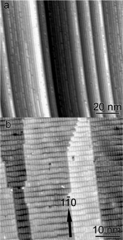
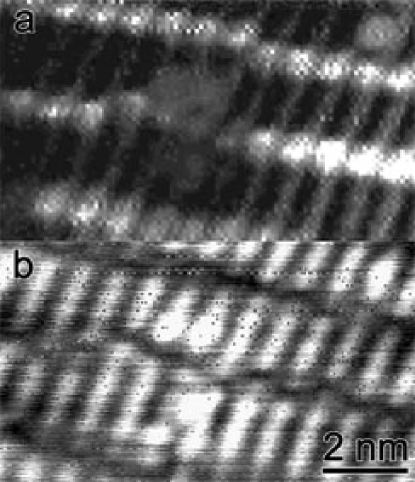
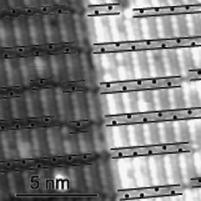
The high index Si(112) surface is tilted 19.5∘ away from the (111) surface towards (001). But the pristine Si(112) surface is not thermodynamically stable, and breaks up into approximately 10 nm wide nano-facets of reconstructed (111)- and (337)-like planes.Baski and Whitman (1995, 1996) An STM image of pristine Si(112) is shown in Fig. 2(a). One might expect that metal deposition on this surface would result in the formation of metallic nanowires in these prepatterned grooves. However, it was shown by Baski et al.Baski and Whitman (1996) that upon deposition and post-annealing of a sub-monolayer amount of Ga the faceted Si(112) surface undergoes a massive restructuring. It returns to its basal (112) orientation, reconstructing as described in the introduction. This preparation procedure of deposition and postannealing of the surface resulted in a reproducible self-limiting surface reconstruction with a unit cell.Jung et al. (1994) A large scale STM image of Ga covered Si(112) is shown in Fig. 2(b). The nanoscale facets have developed into large anisotropic (112) terraces that can extend for up to microns along [10] direction but are less than 100 nm wide. On the terraces, the vacancy lines appear as dark trenches which run perpendicular to the step edges present in this image. Closer inspection reveals that these vacancy lines are not exactly straight, but their position fluctuates around an average position. As discussed below, this is due to the coexistence of and units in the surface and due to the presence of intrinsic fluctuations in the vacancy lines.González et al. (2004)
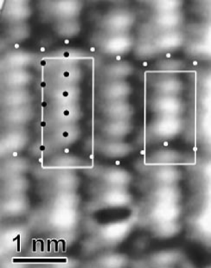
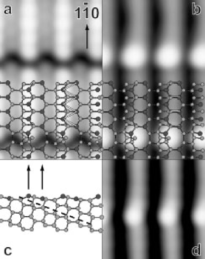
Detailed atomic resolution STM images were acquired to investigate the atomic structure of the Si(112)-Ga surface. In Fig. 3 an atomic resolution empty state STM image is shown. Note that this particular area of the surface shows both and unit cells as indicated in the figure. Two parallel atom rows are observed per unit cell, running in the [10] direction, intersected by the quasi-periodical vacancy lines. Comparing this image with the results of Baski et al.,Baski et al. (1999) we observe the same spacing of the brightest atom rows (i.e. 9.4 Å). Furthermore, the mixed periodicities and the similar LEED pattern (see Refs. Baski et al., 1999 and Jung et al., 1994, respectively), indicate that the same surface reconstruction is studied here. Consequently we conclude that the brightest atom rows in Fig. 3 are the same atom rows as imaged by Baski et al.Baski et al. (1999) (henceforth, the ”step-edge Ga row”). But in addition we observe a atom row lying in between the brighter rows. In terms of the JKP-model, this row of atoms could be interpreted as the Si dangling bond row which might form a quasi 1D band. However, these two parallel atomic lines clearly form a zig-zag pattern as indicated in figures 3 (see also Fig. 13), which results in a structural asymmetry in the vacancy line. This is in contradiction with the JKP-model, which implies mirror plane symmetry with respect to the (10) plane in the vacancy line.
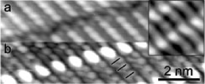
In Fig. 4 a set of registry aligned dual bias images is presented. These images have been recorded simultaneously on the same area of the surface, but with opposite tunneling bias polarities resulting in a set of spatially correlated empty and filled state images. In this case, the empty state image, Fig. 4(a), has suffered from a slight decrease in resolution, as compared with Fig. 3, but the asymmetry in the vacancy line is still visible. In the filled state image, Fig. 4(b), a relatively big, symmetric protrusion prevents a detailed observation of the atomic structure in the vacancy line. As in the empty state image, two parallel atom rows are also visible in the filled state image. They form a ladder structure instead of the zig-zag pattern of the rows observed in the empty state image.
RBS measurements were performed to determine experimentally the amount of Ga at the surface. Integration of the Ga peak in the backscattered He spectrum yielded an amount of Ga atoms per unit cell, to be compared with 5 Ga per unit cell for the JKP-model of Fig. 1.
In summary, these experimental results (STM and RBS) consistently show that the step-edge decorated JKP-model of the Si(112)-Ga surface is at variance with the new experimental observations. Consequently, the intuitive idea of metal adatom step-edge decoration does not seem applicable for the Ga/Si(112) interface.
IV STM image simulations
Extensive DFT calculations were performed to identify the precise atomic structure of the Si(112)-Ga surface. Using the DFT local-orbital hamiltonian of the surface together with non-equilibrium Keldysh Green function techniques,Mingo et al. (1996); Jurczyszyn et al. (2001) we calculated theoretical STM images of these most promising structures, which were then compared with the high resolution experimental STM images. The different Si(112)-Ga structures analyzed in this paper, with Ga-coverages ranging from 5 to 11 Ga atoms per 61 unit cell, have been generated starting from the JKP-model (see Fig. 1), in the following way: (a) replacing some of the Si atoms in the Si-dangling-bond row by Ga atoms (hereafter referred to as Ga terrace atoms); (b) replacing some of the Ga atoms at the step edge by Si atoms; (c) considering also the replacement of Si or Ga atoms on the step-edge and terrace rows by vacancies and the addition of Ga or Si atoms in the vacancy lines. In total, more than 40 new structures were fully relaxed, their surface energies and electronic structures calculated, and their corresponding theoretical STM images obtained. In the following, we compare the theoretical STM images of structures with the lowest total energies; a detailed chemical potential analysis of the total energies is deferred to Section VI.
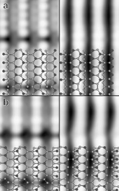
Fig. 5(a) and (b) show two examples of simulated STM images for some of these structural models, with a top view of the corresponding atomic structure superimposed. Fig. 5(a) corresponds to a structural model that contains, per unit-cell, 6 Ga atoms in the terrace row, and 5 Ga atoms plus a vacancy in the step-edge row; in Fig. 5(b) there are 5 Ga and one Si in the terrace row, and 5 Ga plus a vacancy in the step-edge row. The simulated STM images for the different structural models are compared in detail with the experimental high-resolution STM images. For example, Fig. 5(a) (filled state) is similar to the filled-state STM image obtained in Ref. Baski et al., 1999; also the empty-state image of Fig. 5(b) is in good agreement with the experimental STM image shown in Fig. 3. However, a detailed analysis of both empty and filled states images, as well as registry aligned dual images (e.g. Fig. 4), reveal that these models present some inconsistency with the experimental high-resolution information. For example, the structural model of Fig. 5(a) is symmetric with respect to the vacancy line, in disagreement with Fig. 3; in the case of Fig. 5(b) registry aligned dual bias STM images show that the bright protrusion in the filled state image is located in the vacancy line, aligned with the brighter Ga row of the empty state image, while in the simulated filled state-image it appears in between the two Ga rows.
Thus, a detailed comparison of the theoretical STM images for the different structural models with the experimental STM images was performed. From this analysis, we concluded that the correct atomic model for the Si(112)-Ga is the one shown in Fig. 6. In this new structural model there are 10 Ga atoms per unit-cell (to be compared with the RBS determination of Ga atoms), forming two parallel rows, in a zig-zag configuration (see also Fig. 3). The upper row of step-edge Ga atoms adsorbed at the (111)-like step is equivalent to the Ga row in the JKP-model. But the Si dangling bond row in the JKP-model has been replaced by a second row of Ga atoms (henceforth, the ”terrace Ga row”). Each Ga-row contains 5 Ga atoms per unit-cell, i.e. there is a Ga-vacancy in each row. These vacancies are placed at adjacent sites in the (zig-zag) two rows, giving rise to an asymmetry in the vacancy line, see Figs. 6 and 3.
Inside the vacancy lines, missing Ga atoms expose the underlying Si atoms. These Si atoms rebond forming Si-Si dimers on the terraces and Si-Ga dimers along the step edges in each unit cell. Specifically, by rotating a step-edge Si atom toward the step-edge Ga row, this Si atom can rebond to two neighboring Si atoms and a step-edge Ga atom, forming a Si-Ga dimer with the latter. The rebonding of the Si atoms in the vacancy line also implies that the Ga vacancies on both Ga rows must be aligned. In contrast with the tetravalent Si atoms in the step-edge decorated JKP-model, both the trivalent Ga atoms in the three-fold adsorption sites on the (111)-like terraces, and the exposed Si atoms inside the vacancy lines present no unsaturated dangling bonds; the resulting structure (Fig. 6) is fully passivated and the surface is semiconducting.
The calculated theoretical STM images corresponding to this zig-zag model are shown in Fig. 7, with a top view of the structural model superimposed on top. Both the empty state and filled state images are in excellent agreement with the experimental ones (see Fig. 3). It shows that the two atom rows imaged in the empty state STM images, are indeed the step-edge Ga row and the terrace Ga row, ruling out the formation of a Ga-atom step-edge decorated structure. In addition, the asymmetry in the vacancy lines observed experimentally in the empty state, is neatly reproduced in the simulated STM images. In the simulated filled state image, fuzzy lines with a big, symmetric protrusion inside the vacancy line are observed, in agreement with the experimental images. Fig. 7(b) clearly shows that the big protrusion corresponds to the Ga-Si dimer. Furthermore, it shows that the fuzzy lines are originating from a Si-Ga bond on the (111)-like terrace. They form a ladder configuration, in agreement with the atomic resolution experimental image in Fig. 4. The only feature which was not reproduced is the slightly higher apparent height, in the empty state experimental images, of the Ga atoms in the two terrace Ga rows directly adjacent to the vacancy line. Finally, we mention that changing the tunneling conditions in the simulated STM images (tip-sample distance, voltage), the experimental STM images of Ref. Baski et al., 1999 can be recovered, as shown in Fig. 7(d).
V Spectroscopy
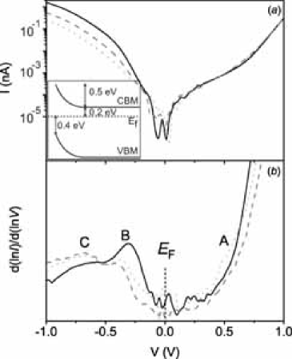
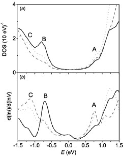
We also have studied this surface reconstruction with scanning tunneling spectroscopy. While imaging the surface with constant tunneling current, at every third data point an curve is measured with the feedback loop switched off during this measurement. In Fig. 8 we have averaged curves measured on the upper atom rows, the lower atom rows, and on the vacancy lines separately (the respective areas being determined from the empty state STM image). This results in three curves, representing the electronic structure on the terrace and step-edge Ga rows, and the electronic structure inside the vacancy line. At bias voltages below the bulk conduction band minimum, the tunneling current is limited by thermionic emission, as is evident from the linear increase of the curve,Sze (1981) up to the conduction band minimum (CBM) at 0.7 V, see Fig. 8(a). Consequently, the bulk valence band maximum (VBM) at the surface should be located at V, implying an upward band bending of eV for this n-type specimen (), and being and eV at the surface, respectively, as shown in the inset of Fig. 8(a). These data are consistent with the measured surface photovoltage in Refs. Yoo et al., 2002; Snijders et al., . In Fig. 8(b) we have plotted the normalized derivative of the three curves (i.e. ), originating from the three different areas within the unit cell. These tunneling spectra are proportional to the local density of states (LDOS) at the respective areas of the sample surface over which the averaging took place (see Refs. Feenstra et al., 1986; Tersoff and Hamann, 1983, 1985). In all curves, there is no DOS at the Fermi level, but a gap of exists between the filled and empty state bands showing that indeed the surface is semiconducting. The tunneling spectra on the two Ga atom rows appears to be similar in shape, whereas the tunneling spectra inside the vacancy line deviates from the former two. The leading edge of the total tunneling spectrum in the filled state spectrum arises from a state (B) that is located mainly inside the vacancy lines at about eV. The two Ga rows feature a broad filled state at higher binding energy (C). In the empty state tunneling spectra the two atom rows show a small shoulder (A) at about eV, just below the bulk CBM. Thus a surface band gap of eV is deduced. These experimental data are entirely consistent with the presence of two equivalent, threefold coordinated rows of Ga atoms at these positions, fully passivating the surface. Notice that we inferred the surface band gap from the separation between peaks A and B using the peak position or centroids, and not the onsets. The justification for this procedure comes from a detailed comparison with theoretical STS data, as will be discussed below.
In addition, we have constructed a -map of the STS measurements. In a -map, the value of the derivative of the -curves at a certain voltage is plotted as a two-dimensional image, with the and coordinates corresponding to the topographic STM image. In Fig. 9(a) the derivative of the -curves at -0.31 V is plotted, the corresponding empty state STM image is shown in Fig. 9(b). Indeed, the largest slope in the -curves at -0.31 V is located inside the vacancy lines (i.e. here the largest increase in tunneling current is observed, corresponding to the largest LDOS as compared to the LDOS at this specific energy at other locations on the surface). Only a very small intensity variation is observed perpendicular to the atom rows, consistent with the similar filled state tunneling spectra on the two Ga rows in Fig. 8(a).
From the structural model and its spatially resolved DOS, theoretical STS curves were calculated, see Fig. 10(b). As for the STM images, these results are obtained using the LO-DFT Fireball96 hamiltonian of the surface and the Keldysh Green function approach. The corresponding calculated LDOS of the zig-zag model, averaged over different areas is shown in Fig. 10(a) (a broadening of 0.1 eV has been used). The calculated STS curves shown in Fig. 10(b) were obtained by placing the tip over the respective areas, calculating the current as a function of a voltage sweep using the calculated LDOS (Fig. 10), and averaging over the areas of interest. The Fireball96 local orbital calculations employ a minimal basis set, resulting typically in band gaps that are too large. Nonetheless, excellent qualitative agreement exists between the calculated STS curves and normalized derivatives of the experimental STS curves (Fig. 8(b)). The calculated LDOS and STS curves confirm that the large peak B just beneath the band gap indeed is mainly associated with states that are located on the Si-Ga dimer inside the vacancy lines. The two Ga rows contribute almost equally to a broad peak in the DOS at higher binding energy (C) and a small shoulder in the DOS just above the band gap (A), in full agreement with the normalized derivative of the tunneling spectra in Fig. 8(b). The empty state DOS is very similar for both Ga rows. Consequently the Åhigher appearance of the Ga atoms at the step edge in the empty state image is due to their on average higher atomic positions, and thus the empty state STM image reflects the real surface topography at these voltages.
We have calculated the surface bandstructure using both the LO and PW-DFT methods, within the LDA for exchange-correlation contributions. While the LO calculation overestimates the value of the bulk band gap, the PW calculation typically underestimates the band gap. In the LO bandstructure (not shown) a surface state band gap of 1.2 eV is obtained between the states A and B, while the separation between peaks A and B in the calculated STS is close to 1.4 eV. This suggests that in order to measure the band gap, it is reasonably accurate to use the peak positions instead of the (poorly defined) peak onsets in the experimental curves. The observed splitting between A and B in the experimental curves is eV indicating that the experimental band gap is eV. Fig. 11 shows the bandstructure as calculated with the PW-DFT code, showing a surface band gap of 0.77 eV between states A and B.111Note that the bulk projected gap for the PW (LDA) calculation is not equal to eV, as a fully converged PW (LDA) calculation should give. This is caused by the fact that the bands are plotted along symmetry directions in the surface Brillouin zone that do not contain the k-point corresponding to the bulk Si CBM. The calculations place filled state B slightly above the VBM, in agreement with the experimental observation. On the other hand, the empty surface state A is located at or slightly above the CBM according to the PW-DFT calculations, while experimentally state A appears slightly below the bulk CBM; see Fig 8(b). The PW gap of 0.77 eV is comparable to the experimental band gap of 0.8 eV. However, the precise location of state A in the calculations directly affects the value of the band gap.
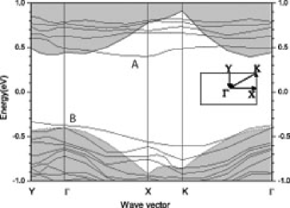
Despite the fact that the Ga/Si(112) overlayer appears to be quasi two-dimensional in atomic structure, the electronic structure of this overlayer is quasi one-dimensional. The Ga-atom induced surface band A disperses around the -point minimum in the upper part of the band gap. The dispersion of this band near the -point yields an effective mass of along the direction, and along . This indicates a quasi-one-dimensional dispersion. This Ga-band is initially empty but could perhaps be populated in a controllable way, using a biased gate electrode, or a heavily n-type doped substrate, making the Si(112)-Ga surface a promising system for the experimental study of electron transport in one dimensional atomic wires.
VI Competing structures
The discussion above shows that, to elucidate the precise atomic structure of a complex surface like Si(112)-Ga from the comparison of theoretical and experimental STM images, it is necessary to use high-resolution experimental STM images, including registry aligned dual bias information and STS data, combined with state of the art theoretical STM simulations. These simulations were performed on the subset of possible structures that were deemed most realistic on the basis of total energy considerations. In this section, we explore the relative stability of the various structures, which gives a more physical basis to the proposed structural model.
In general, the precise stoichiometry of the surface is not known, and thus the analysis of the relative stability of different structural models requires the calculation of the surface energy as a function of the different chemical potentials.
VI.1 Chemical potential analysis
For the analysis of the relative stabilities of the various structures, we need to calculate the surface energy , where is the total energy per unit-cell, , are the Ga and Si chemical potentials, and , are the number of Ga and Si atoms in the unit-cell. For we use the total energy (per atom) of bulk-Si (i.e. the surface is in equilibrium with the substrate). The value of is not determined by the substrate, but it can be estimated analyzing the experimental conditions (see below).
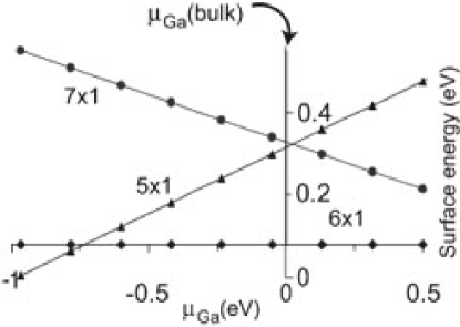
Fig. 12 shows the surface energy as a function of . In this figure we use the structural model of Fig. 6 as reference, and plot for some of the most promising models, as calculated with the PW code (Castep). In order to estimate the value of we have to analyze the experimental conditions of the Ga deposition. In the ”one-step” process the ()-phase is formed under a Ga flux from the effusion cell with the sample held at a temperature of K. At this temperature the incoming flux of Ga atoms is balanced by a flux of Ga atoms desorbing from the surface, thus establishing a quasi-equilibrium. This allows us to relate the chemical potential in the effusion cell with the chemical potential at the sample. The chemical potential in the effusion cell may be approximated by the total energy of bulk-Ga, , i.e. the Ga vapor in the effusion cell is in equilibrium with the solid.222The chemical potential of liquid Ga is approximated by the chemical potential of solid, bulk Ga at T=0K. Finite temperature corrections which include the enthalpy of melting and the integrated heat capacity are very small ( eV) and have been neglected.
Considering also the equilibrium between the sample and the Ga vapor in contact with the sample, we can estimate the chemical potential at the sample
where is the Ga vapor pressure in the effusion cell and the Ga vapor pressure at the sample. Since the effusion cell flux is proportional to its vapour pressure, , times the cell aperture area, and the sample flux is also proportional to its corresponding vapour pressure, , times the sample area, we conclude that , and eV. In Fig. 12 we see that for this range of the structural model of Fig. 6 presents the lowest surface energy . This result strongly supports our conclusion that the structural model for the Si(112)-Ga surface is the one depicted in Fig. 6.
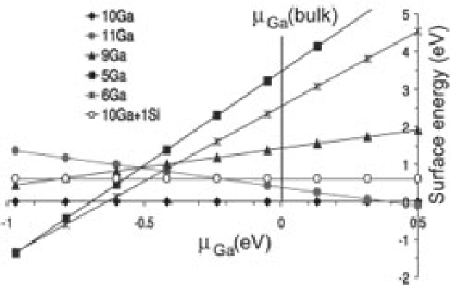
Comparing our model with the step-edge decorated JKP-model, an important difference is that the new structural model (Fig. 6) presents no partially-filled dangling bonds as discussed above. The stability of the new model is related to the full passivation of the substrate, removing all dangling bonds, and the associated decrease in surface free energy. The results shown in Fig. 12 suggest, however, that the JKP-model might be stabilized for very low values. We should stress that our theoretical analysis has been directed to search for surface atomic structures that could explain the experimental results (STM and RBS) for the Si(112)-Ga surface, and thus surface structures with lower Ga coverages, that should be favored for low values have not been analyzed as thoroughly as those with coverages close to 9-10 Ga atoms/ unit cell. Nevertheless, we may perform a simple analysis, comparing the surface energy of the step-edge decorated JKP-model, with the surface energy of a simple hypothetical surface: half the surface is covered with the structure of Fig. 6 (i.e. both step-edge and terrace Ga rows) while the other half consists of clean Si(112). Both the step-edge decorated JKP system and this hypothetical half-half case present the same Ga coverage and thus the same behavior of as a function of (i.e. the same slope in Fig. 12). This comparison reveals that the hypothetical case is lower in energy (by 0.7 eV/(10 Ga atoms), for all values, showing that the step-edge decorated case is unlikely to be stabilized at lower Ga coverage, and phase separation into bare Si(112) and the Si(112)-Ga zig-zag surface will occur instead. Note that the facetting of the unstable Si(112) surface, which was not accounted for in this calculation, would increase this energy difference, making phase separation even more favorable compared to the step-edge decorated JKP-model.
Another possible scenario for obtaining a step-edge decorated Ga row would be to use the experimentally observed fully passivated Si(112)-Ga surface (Fig. 6) as starting point, and try to kinetically stabilize a metastable step-edge decorated structure by selectively desorbing the Ga atoms from the terraces. Experimentally, this might happen in the ’two-step’ preparation procedure, see Section II. We have studied this possibility by calculating desorption energies of terrace and step-edge Ga atoms from the Si(112)-Ga surface (Fig. 6). In particular, we have considered removing the Ga atoms close to the vacancy line as well as the replacement of those Ga atoms by Si atoms. In both cases the desorption energies are lower by eV for step-edge Ga atoms than for Ga atoms on the terraces. This result suggests that a metastable step-edge decorated structure likely can not be achieved by thermally desorbing the Ga terrace atoms.
VI.2 Intrinsic structural disorder
In the experimental STM images, the vacancy lines are not exactly straight, but some meandering is observed, as shown in Fig. 13 (see also Figs. 2(b) and Fig. 3). The new structural model is able to fully explain the experimentally observed meandering.González et al. (2004) It was proposed by Erwin et al.Erwin et al. (1999) that this meandering of the vacancy lines could be explained by the co-existence of and unit cells on the surface. This results in occasional steps in the vacancy lines, equivalent to the observed meandering of the dimer-vacancy lines on the Ge covered Si(001) surfaces.Chen et al. (1994) We have analyzed the stability of the zig-zag structural model as a function of the longitudinal periodicity. Fig. 14 shows the surface energies of this model for different periodicities: , and . The surface corresponds to 4 Ga atoms in each Ga-row between vacancy lines, while the surface presents 6 Ga atoms in each row between vacancy lines. For our estimated range of the surface presents the lowest , while the is only 0.1-0.2 eV higher, per unit-cell. This small energy difference should lead to the experimental observation of unit cells. Indeed these unit cells are frequently observed in the experimental images, see Fig. 13. It thus appears that the predictions from the 1D Frenkel-Kontorova model regarding the vacancy-line spacing in the step-edge decorated structureErwin et al. (1999) also apply to the quasi 2D zig-zag arrangement of Ga atoms presented here. This conclusion is not very surprising as it was concluded in Ref. Erwin et al., 1999 that the strain induced by the size difference of Ga and Si completely dominates the energetics of the periodicities. Apparently this conclusion still holds when an extra Ga row is added.
However, careful investigation of the experimental images reveals that the meandering of the vacancy lines as observed in Fig. 2 is not only due to the competing longitudinal periodicities. Instead, for large sections of the surface, the terrace Ga rows are perfectly periodic in the direction with (n-1) Ga atoms per terrace Ga row in the n unit cell. But in these ordered sections the number of Ga atoms in the step-edge Ga rows appears to fluctuate between n-2 and n. The proposed structural model perfectly explains these intrinsic fluctuations (i.e. fluctuations within a n domain); they are related to the orientation of the Si-Ga dimer in the step-edge rows. The twofold symmetry of the 112 substrate in the [10] direction is broken by the Si-Ga dimers, resulting in two degenerate orientations of these dimers. The energy associated with interchanging the atoms of a Si-Ga dimer has been calculatedGonzález et al. (2004) to be less than 10 meV per unit cell. This small energy difference explains the appearance of frequent meandering in the aligned vacancies in the step-edge Ga rows, thus accounting for the majority of the fluctuations in the vacancy lines observed in the experimental images. The absence of these fluctuations in the filled state images (compare Figs. 4(a) and (b) and also Figs. 9(a) and (b)) is the result of the fact that the bright protrusion in the vacancy line appears in the center of the Ga-Si dimer, making its appearance insensitive to the orientation of the Ga-Si dimer.
VII Summary and conclusions
The reconstruction of Ga on vicinal Si(112) was studied with STM, STS, RBS, and extensive DFT calculations. High resolution STM experiments revealed an asymmetry in the vacancy lines of the Si(112)-Ga surface that is inconsistent with the JKP-model of step-edge decoration. STS measurements also rule out formation of quasi 1D metal wires while RBS experiments indicated a Ga coverage twice as large as previously inferred from the JKP model. Extensive DFT calculations were used to analyze the relative stability of more than forty structures, taking the chemical potential of the Ga adsorbate into account. Theoretical STM images were calculated for the most promising structures and compared in detail with the experimental STM images.
A new structure emerged containing 10 Ga atoms per unit cell. The Ga atoms decorate the step edge and passivate the terrace atoms, thereby forming a zig-zag pattern. Excellent agreement between experimental and theoretical STM and STS data confirmed the validity of the proposed zig-zag model and demonstrate the power of such a comparison. Ga atoms are threefold coordinated and Si dangling bonds are all passivated so the surface is semiconducting. The ”broken bond orbitals” inside the vacancy lines rebond to form Si-Ga and Si-Si dimers. The observed meandering of the vacancy lines originates from thermal fluctuations between the two symmetry-degenerate orientations of the Si-Ga dimer, in conjunction with thermal fluctuations between competing and units.
While step-edge decoration of vicinal metal surfaces works,Gambardella et al. (2002) the observed drive toward chemical passivation suggests that step-edge decoration of vicinal semiconductors is not a viable method to produce 1D metal wires. Although this general conclusion remains to be tested further, it is clear that partially-filled dangling bonds on the terraces of vicinal surfaces are always greatly reduced in number or eliminated altogether in the reconstruction.
As shown in this paper, predictive calculations along these lines should always take into account the chemical potential of the adsorbate. The latter depends on the experimental preparation conditions (see e.g. equation (4)). Successful prediction of systems with perfect 1D metal adatom step-edge decoration could facilitate the quest for the experimental realization of Luttinger liquids in such systems, possibly enabling a convincing proof of spin-charge separation with angle resolved photoemission spectroscopy.
VIII Acknowledgements
This work is part of the research programme of the ’Stichting voor Fundamenteel Onderzoek der Materie (FOM)’, which is financially supported by the ’Nederlandse Organisatie voor Wetenschappelijk Onderzoek (NWO)’. This work was sponsored in part by the NSF under contract No. DMR-0244570, the Ministerio de Ciencia y Tecnología (Spain) under grants No. MAT2001-0665 and MAT2004-01271. One of us, S.R., wishes to acknowledge the Royal Netherlands Academy of Arts and Sciences. We thank T.M. Klapwijk for his stimulating support, and the AMOLF institute in Amsterdam for performing the RBS experiments. Oak Ridge National Laboratory is managed by UT-Battelle, LLC, for the US Department of Energy under contract No. DE-AC-05-00OR22725.
References
- Postma et al. (2000) H. W. C. Postma, M. de Jonge, Z. Yao, and C. Dekker, Phys. Rev. B 62, R10653 (2000).
- Grioni et al. (1999) M. Grioni, I. Vobornik, F. Zwick, and G. Margaritondo, J. Electron Spectrosc. Relat. Phenom. 100, 313 (1999).
- Voit (1994) J. Voit, Rep. Prog. Phys. 58, 977 (1994).
- Himpsel et al. (2001) F. J. Himpsel, K. N. Altmann, R. Bennewitz, J. N. Crain, A. Kirakosian, J.-L. Lin, and J. L. McChesney, J. Phys.: Condens. Matter 13, 11097 (2001).
- Crain et al. (2004) J. N. Crain, J. L. McChesney, F. Zheng, M. C. Gallagher, P. C. Snijders, M. Bissen, C. Gundelach, S. C. Erwin, and F. J. Himpsel, Phys. Rev. B 69, 125401 (2004).
- Starowicz et al. (2002) P. Starowicz, O. Gallus, T. Pillo, and Y. Baer, Phys. Rev. Lett. 89, 256402 (2002).
- Segovia et al. (1999) P. Segovia, D. Purdie, M. Hengsberger, and Y. Baer, Nature 402, 504 (1999).
- Yeom et al. (1999) H. W. Yeom, S. Takeda, E. Rotenberg, I. Matsuda, K. Horikoshi, J. Schaefer, C. M. Lee, S. D. Kevan, T. Ohta, T. Nagao, et al., Phys. Rev. Lett. 82, 4898 (1999).
- Ahn et al. (2004) J. R. Ahn, H. W. Yeom, E. S. Cho, and C. Y. Park, Phys. Rev. B 69, 233311 (2004).
- Bunk et al. (1999) O. Bunk, G. Falkenberg, J. H. Zeysing, L. Lottermoser, R. L. Johnson, M. Nielsen, F. Berg-Rasmussen, J. Baker, and R. Feidenhans l, Phys. Rev. B 59, 12228 (1999).
- Robinson et al. (2002) I. K. Robinson, P. A. Bennett, and F. J. Himpsel, Phys. Rev. Lett. 88, 096104 (2002).
- González et al. (2004) C. González, P. C. Snijders, J. Ortega, R. Pérez, F. Flores, S. Rogge, and H. H. Weitering, Phys. Rev. Lett. 93, 126106 (2004).
- Crain et al. (2003) J. N. Crain, A. Kirakosian, K. N. Altmann, C. Bromberger, S. C. Erwin, J. L. McChesney, J.-L. Lin, and F. J. Himpsel, Phys. Rev. Lett. 90, 176805 (2003).
- Ahn et al. (2003) J. R. Ahn, H. W. Yeom, H. S. Yoon, and I.-W. Lyo, Phys. Rev. Lett. 91, 196403 (2003).
- Matsuda et al. (2003) I. Matsuda, M. Hengsberger, F. Baumberger, T. Greber, H. W. Yeom, and J. Osterwalder, Phys. Rev. B 68, 195319 (2003).
- Kanagawa et al. (2003) T. Kanagawa, R. Hobara, I. Matsuda, T. Tanikawa, A. Natori, and S. Hasegawa, Phys. Rev. Lett. 91, 036805 (2003).
- Jung et al. (1993) T. M. Jung, R. Kaplan, and S. M. Prokes, Surf. Sci. 289, L577 (1993).
- Jung et al. (1994) T. M. Jung, S. M. Prokes, and R. Kaplan, J. Vac. Sci. Technol. A 12, 1838 (1994).
- Yater et al. (1995) J. E. Yater, A. Shih, and Y. U. Idzerda, Phys. Rev. B 51, R7365 (1995).
- Baski et al. (1999) A. A. Baski, S. C. Erwin, and L. J. Whitman, Surf. Sci. 423, L265 (1999).
- Erwin et al. (1999) S. C. Erwin, A. A. Baski, L. J. Whitman, and R. E. Rudd, Phys. Rev. Lett. 83, 1818 (1999).
- Yoo et al. (2002) K. Yoo, S. J. Tang, P. T. Sprunger, I. Benito, J. Ortega, F. Flores, P. C. Snijders, M. C. Demeter, and H. H. Weitering, Surf. Sci. 514, 100 (2002).
- Baski and Whitman (1996) A. A. Baski and L. J. Whitman, J. Vac. Sci. Technol. B 14, 992 (1996).
- Glembocki and Proke (1997) O. J. Glembocki and S. M. Proke, Appl. Phys. Lett. 71, 2355 (1997).
- Demkov et al. (1995) A. A. Demkov, J. Ortega, O. F. Sankey, and M. P. Grumbach, Phys. Rev. B 52, 1618 (1995).
- Sankey and Niklewski (1989) O. F. Sankey and D. J. Niklewski, Phys. Rev. B 40, 3979 (1989).
- (27) CASTEP 4.2 Academic version, licensed under the UKCP-MSI Agreement, 1999.
- Mingo et al. (1996) N. Mingo, L. Jurczyszyn, F. J. Garcia-Vidal, R. Saiz-Pardo, P. L. de Andres, F. Flores, S. Y. Wu, and W. More, Phys. Rev. B 54, 2225 (1996).
- Jurczyszyn et al. (2001) L. Jurczyszyn, J.Ortega, R. Pérez, and F. Flores, Surf. Sci. 482-5, 1350 (2001).
- Blanco et al. (2004) J. M. Blanco, C. González, P. Jelínek, J. Ortega, F. Flores, and R. Pérez, Phys. Rev. B 70, 085405 (2004).
- Blanco et al. (2005) J. M. Blanco, C. González, P. Jelínek, J. Ortega, F. Flores, R. Pérez, M. Rose, M. Salmeron, J. Méndez, J. Wintterlin, et al., Phys. Rev. B 71, 113402 (2005).
- Baski and Whitman (1995) A. A. Baski and L. J. Whitman, Phys. Rev. Lett. 74, 956 (1995).
- Sze (1981) S. M. Sze, Physics of Semiconductor Devices (John Wiley and Sons, 1981).
- (34) P. C. Snijders, J. N. Crain, J. L. McChesney, M. C. Gallagher, and F. J. Himpsel, unpublished data.
- Feenstra et al. (1986) R. M. Feenstra, J. A. Stroscio, and A. P. Fein, Surf. Sci. 181, 295 (1986).
- Tersoff and Hamann (1983) J. Tersoff and D. R. Hamann, Phys. Rev. Lett. 50, 1998 (1983).
- Tersoff and Hamann (1985) J. Tersoff and D. R. Hamann, Phys. Rev. B 31, 805 (1985).
- Chen et al. (1994) X. Chen, F. Wu, Z. Zhang, and M. G. Lagally, Phys. Rev. Lett. 73, 850 (1994).
- Gambardella et al. (2002) P. Gambardella, A. Dallmeyer, K. Maiti, M. C. Malagoli, W. Eberhardt, K. Kern, and C. Carbone, Nature 416, 301 (2002).