High-sensitivity microwave vector detection at extremely low-power levels for low-dimensional electron systems
Abstract
We present a high-sensitivity microwave vector detection system for studying the low-dimensional electron system embedded in the gaps of a coplanar waveguide at low temperatures. Using this system, we have achieved 0.005% and 0.001° resolutions in amplitude and phase variations, respectively, at 10 GHz in a magnetotransport measurement on a quantum-wire array with an average signal power less than 75 dBm into the sample at 0.3 K. From the measured phase variation, we can distinguish a very tiny change in the induced dipole moment of each quantum wire.
pacs:
07.05.Fb, 07.57.Ac, 07.57.Kp, 73.50.Mx, 73.21.HbCoplanar waveguides (CPW’s) have been successfully used as broadband sensors in investigating the high-frequency magnetotransport phenomena of low-dimensional electron systems (LDES’s), such as two-dimensional electron systems (2DES’s),Engel1993 ; Li1997 ; Ye2002 ; Lewis2002 ; Chen2003 and anti quantum dots (QD’s),Ye2002B etc. In these works, a commercial vector network analyzer (VNA) is the major tool to measure the variation of the propagation constant, including the attenuation constant () and the phase constant (), of the CPW that containing the active LDES in the gaps between the metal electrodes. From and one can extract the longitudinal conductivity ()Engel1993 (both real and imaginary parts) of the LDES. However, since the microwave power delivered to samples at temperature () below few hundred mK must be very low, the resolution of the data becomes very poor, especially for the phase part. Thus in most of the previous studies using CPW sensors, they only presented Re{} data derived from and discarded the phase part. Even though Hohls et al.Hohls2001 and Lewis et al.Lewis2001 have addressed the Im{} behavior in the integer quantum Hall (IQH) regime based on other techniques, still, the resolution of Im{} is mediocre due to the constrain of VNA’s. Nevertheless, Im{}, proportional to the change of the real part of dielectric constant, gives important information about the electric polarization, that is of special interest in the case of QD’s, quantum wires (QW’s), or 2DES’s at high magnetic fields (). Furthermore, the relatively small effective area of QD’s or QW’s compared to 2DES samples leads to a very small signal variation (or dynamic range), that makes the conventional VNA measurement very difficult and impractical.
In this letter, we present a new detection scheme and the instrumental implementation, which can resolve very small variations not only in the amplitude but also the phase of an extremely low-power-level microwave signal traveling through a CPW with LDES’s embedded in the gaps while some external sample parameters, such as the applied magnetic field () or , etc., is changed. The data of a low- magnetotransport measurement on a QW-array sample manifest the high-resolution capability of this system.
A simplified schematic diagram to illustrate the principle of phase detection by a phase-lock loopPLL (PLL) is depicted in Fig. 1 (a). The CPW sample is connected to a PLL through two semirigid coaxial cables of total length . The PLL will force the total phase change (), including the phase change of the semirigid cables () and the CPW sample (), to be 0 by tuning the frequency () of the voltage-controlled oscillator (VCO) during the experiments, that is, , or . Hence can be obtained directly from the frequency change () of VCO via
| (1) |
where is the phase velocity of the signal in the cable. The result can be expressed as the product of the change of the angular frequency () and the delay time () of the connecting cables with a different sign.
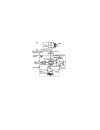
A complete block diagram, including the pulse handling circuits, the microwave PLL, and the amplitude readout circuit, together with the CPW sample in a cryogenic environment, is shown in Fig. 1 (b). The microwave part of this system is basically a pair of homodyne detectors (mixers) with reference signals of quadrature phase difference. One of the mixers with 0° reference (LO1), used as the phase sensitive detector (PSD), has zero output (IF1) forced by the PLL, while the other one with 90° reference (LO2) has an output (IF2) proportional to the amplitude of the signal.
Besides homodyne detection we employ a double-pulse modulation scheme to detect and average the microwave signal. A short pulse train with a 0.22 s pulse width and a 0.110% duty cycle, provided by a pulse generator and gated by a slow square-wave TTL signal with a period of 110 ms from a lock-in amplifier, modulates the microwave signal sent to the sample. A time-delayed pulse with a 0.11 s pulse width triggered by the modulating pulses controls a sample-and-hold (S&H) circuit that samples the IF output of the microwave mixer. The holding capacitor in the S&H circuit is discharged through an analog switch when the TTL gating signal is low. Finally the lock-in amplifier reads the output of the S&H circuit. There are two sets of pulse averaging circuits, one for the PLL and the other for the amplitude readout. Note that the time constant of the lock-in amplifier for the PLL is about 130 ms, in contrast to 300 ms or 1 s for the amplitude readout part. The average of the PSD output (IF1) is sent to an integrator (loop filter of PLL) with a time constant of 26.3 ms. The output of the integrator connects to the FM input of the microwave source (VCO), thus closing the PLL. In fact this PLL system is modified from what people used in surface-acoustic-wave detection experiments,Wixforth1989 but with improved pulse averaging and amplitude detection methods.
We use three sets of microwave modules to cover the frequency from about 60 MHz to 18 GHz. The details of our instrumentations and circuit designs will be published elsewhere. To gain an idea of the detection limit, we tested our system with only an 11 m semirigid cable connected to the PLL without samples. The input microwave signal is attenuated down to 70 dBm peak power, and less than 90 dBm in average. The background phase fluctuation we obtain in this test is less than 0.0003° (root-mean-squared value) for 6 GHz and 0.006° for 618 GHz, which is remarkably low for such a low-power signal. In fact, the signal power reaching the low-noise amplifier (LNA) is even lower than the input value claimed above due to the loss of the cable, which is about 9 dB at 1 GHz and raises to 41 dB at 10 GHz. This may explain why the noise in phase increases at high frequencies. The resolution with a low- sample loaded is slightly worse due to the loss of the sample and extra noise from the cryogenic environment. The resolution of the amplitude readout for a small-variation signal can be enhanced by the use of the ”offset” and ”expand” functions of the lock-in amplifier.lockin
In the following we will present measured results for a QW array sample to demonstrate the resolving power of this method. The sample is fabricated from a standard MBE-grown modulation-doped GaAs/AlGaAs heterostructure containing a 2DES, which is 150 nm under the surface. The 2DES has a mobility of about 1.5 cmVs at 4K, and a density of 1.1 cm-2. Before evaporating the Cr/Au(10/300 nm) metal layers for the CPW pattern, we etch away the 2DES part underneath. The widths of the center conductor and the gap of the 50 CPW are 36 m and 23 m, respectively. A meandering patternEngel1993 is used to increase the effective length of the CPW. Subsequently we pattern the 2DES left in the gap into about 7000 identical QW mesas, each of 0.7 m wide and 20 m long, by using e-beam lithography and chemical etching [Fig. 2 (a)]. The QW’s, parallel to the propagating direction of microwave signals, occupy only about 6 mm in length of the straight sections of the meandering CPW.
The CPW sample is immersed in liquid 3He (0.3 K) with applied perpendicular to the sample surface. The total time delay given by the connection cables and microwave modules is 51.1 ns. From Eq. 1, this time delay multiplied by gives the phase change () of the CPW sample. Here can be either obtained from the output voltage of the integrator in the PLL scaled with the FM deviation setting of the VCO, or measured directly with a microwave counter. The peak power of the pulsed microwave signals is 50 dBm (about 66 dBm in average) at the input end of the semirigid cable.
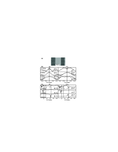
Figure 2 (b) displays low-field results for both directions of . Besides the apparent Shubinkov-de-Hass oscillations, we can observe additional intriguing features for below 0.2 T. For frequency higher than few GHz, the high- data exhibit behaviors similar to a 2DES, showing IQH states. The SdH oscillations become less pronounced at lower and even completely disappear below 600 MHz. In Fig. 2 (c), the data are shown up to 11 T. An extra adsorption peak appears at 6 T associated with a unique phase change nearby for 255 MHz, and moves to lower for higher , indicating that this feature relates to the edge magnetoplasmaGrodnensky1994 (EMP) excitations. More detailed data and explanation of these interesting results will be published separately. Here we will emphasize mainly the resolution of the measurements and also the polarization of each QW that can be extracted from our data.
The background noise of the data shown in Fig. 2 (b) and (c) is extremely low. The amplitude and phase fluctuations in and data are less than 0.003% and 0.001° for 10 GHz, and 0.05% and 0.03° for 10 GHz, respectively. These resolution limits actually depend on the power reaching the LNA, which is dependent due to the loss of the sample and the semirigid cables. The average power into the sample and into the LNA are about -70 dBm and -76 dBm at 1 GHz, and down to -80 dBm and -107 dBm at 14 GHz, respectively. Moreover, the 0.3 % scale bar in the plot is equivalent to only 53 nS 2D conductivity in average, which is very small compared to the signal levels in previous studies.Engel1993 ; Li1997 ; Ye2002 ; Lewis2002 ; Chen2003 ; Ye2002B
The susceptibility of each QW and can be relatedpeqderive by where is the total number of QW’s, the characteristic impedance of the CPW, and a length scale related to the distribution of the tangential electric field () on the surface and the geometry of the CPW. The induced dipole moment of each QW segment, , is then . For our CPW structure, is about 21 m. The value corresponding to the 0.2° scale bar in Fig. 2(c) for 255MHz is about 3 F/m2. For a signal of 51.5 dBm peak power, we can estimate accordingly to be about 3 Cm, equivalent to about 17 electrons being transferred across a 0.1 m effective QW width, assuming a 0.3 m depletion length near each edge.
Finally, we want to discuss the effect of the cable length and related instrumental considerations. Usually as we increase , the sensitivity in phase is increased according to Eq. 1, and so is the loop gain of the PLL. However, if is too big, the PLL will have a very small capture range, and the effect of noise and drift in electronic components become serious. In addition, high-frequency signals will suffer a very severe loss.
In conclusion, we have developed and demonstrated a high-sensitivity vector detection system for very low-power microwave signals used in a CPW broadband sensor. This system is a very powerful tool in studying the dynamic behaviors, including the electric polarizations, of LDES’s at low temperatures.
This work was supported by National Science Council of Republic of China.
References
- (1) L. W. Engel, D. Shahar, C. Kurdak, and D. C. Tsui, Phys. Rev. Lett. 71, 2638 (1993).
- (2) C.-C. Li, L.W. Engel, D. Shahar, D.C. Tsui, and M. Shayegan, Phys. Rev. Lett. 79, 1353 (1997).
- (3) P. D. Ye, L. W. Engel, D. C. Tsui, R. M. Lewis, L. N. Pfeiffer, and K. West, Phys. Rev. Lett. 89, 176802 (2002).
- (4) R. M. Lewis, P. D. Ye, L. W. Engel, D. C. Tsui, L. N. Pfeiffer, and K. W. West, Phys. Rev. Lett. 89, 136804 (2002).
- (5) Y. Chen, R. M. Lewis, L. W. Engel, D. C. Tsui, P. D. Ye, L. N. Pfeiffer, and K. W. West, Phys. Rev. Lett. 91, 016801 (2003).
- (6) P. D. Ye, L. W. Engel, D. C. Tsui, J. A. Simmons, J. R. Wendt, G. A. Vawter, and J. L. Reno, Phys. Rev. B 65, 121305 (2002).
- (7) F. Hohls, U. Zeitler, and R. J. Haug, Phys. Rev. Lett. 86, 5124 (2001).
- (8) R. M. Lewis and J. P. Carini, Phys. Rev. B 64, 073310 (2001).
- (9) For the design of PLLs, please see, e.g., Roland E. Best, Phase-Locked Loops, 5th ed. (McGraw-Hill, Inc., 2003).
- (10) A. Wixforth, J. Scriba, M. Wassermeier, J. P. Kotthaus, G. Weimann, and W. Schlapp, Phys. Rev. B 40, 7874 (1989).
- (11) SR830 from Stanford Research Systems, Inc., Sunnyvale, CA.
- (12) I. Grodnensky, D. Heitmann, K. v. Klitzing, K. Ploog, A. Rudenko, and A. Kamaev, Phys. Rev. B 49, 10778 (1994).
- (13) This equation can be derived simply by equating the energy stored in the field for the electric dipole moment of all the QW’s, , and the energy increment due to change of the effective capacitance per unit length, . The length scale can be shown to be , where is the capacitance of the CPW if the substrate is replaced by air, and is the average of square of voltage signal over square of tangential field on the surface across the gap of the CPW.