Instrumentation of a high-sensitivity microwave vector detection system for low-temperature applications
Abstract
We present the design and the circuit details of a high-sensitivity microwave vector detection system, which is aiming for studying the low-dimensional electron system embedded in the slots of a coplanar waveguide at low temperatures. The coplanar waveguide sample is placed inside a phase-locked loop; the phase change of the sample may cause a corresponding change in the operation frequency, which can be measured precisely. We also employ a double-pulse modulation on the microwave signals, which comprises a fast pulse modulation for gated averaging and a slow pulse modulation for lock-in detection. In measurements on real samples at low temperatures, this system provides much better resolutions in both amplitude and phase than most of the conventional vector analyzers at power levels below -65 dBm.
pacs:
07.05.Fb, 07.57.Ac, 07.57.Kp, 73.50.Mx, 73.21.HbI Introduction
In the study of dynamic magnetotransport behaviors of low-dimensional electron systems (LDESs), such as two-dimensional electron systems (2DESs),Engel1993 ; Li1997 ; Ye2002 ; Lewis2002 ; Chen2003 quantum wires (QWs)Grodnensky1994 , and anti quantum dots (QDs),Ye2002B a microwave vector detection system, which can measure both the amplitude and the phase variations of the signals under the influence of the LDESs in magnetic fields, is indispensable. Usually people use a conventional vector network analyzer (VNA) as such a detection system by virtues of its expediency and broadband characteristics. The LDES under test can be either embedded in the slots of a coplanar waveguide (CPW),Engel1993 ; Li1997 ; Ye2002 ; Lewis2002 ; Chen2003 ; Ye2002B attached to a resonator,Lewis2001 or directly connected to a coaxial cable;Hohls2001 then the transmission or reflection property can be measured, and the transport properties of the LDES can be extracted therefrom, as the external magnetic field (), or the temperature () changes. However, since in most of these studies the LDES is placed in a very cold environment with temperature () below 4.2 K, or even down to several tens of minikelvins, the power of the excitation signal must be very low, normally below 60 dBm, to avoid joule heating. Moreover, the power reaching the detection system is even lower due to the loss of coaxial cables and the sample itself. Hence the resolution of the data, in particular the phase part, becomes very poor.
In this article, we present the instrumentation and the details of circuit design of a very-high-sensitivity vector detection system,Hsieh2004 incorporating phase-locked loop (PLL) and double pulse techniques. Here we mainly emphasize on the application of this system to the study of LDESs embedded in the slots of a CPW, which have been successfully used as broadband sensors.Engel1993 ; Li1997 ; Ye2002 ; Lewis2002 ; Chen2003 ; Ye2002B Our method is especially useful for the case of QDs or QWs, whose relatively small effective area compared to 2DES samples usually results in a very small variation on the transmission coefficient of the CPW sample, and makes the conventional VNA measurement very formidable and impractical.
In a typical modern VNA, a PLL is only used in the very front end of its superheterodyne receiverWhite1993 to make the local oscillator (LO) of the first-stage mixers follow the reference signal from the tracking source, and thus to preserve the phase information in the detected signal. In contrast, we put the CPW sample under test in the high-frequency signal path of a PLL, which is renowned for its phase sensitivity, and obtain a great improvement in the phase resolution. As a matter of fact, the PLL-based phase detection technique has been applied in the study of 2DESs using surface acoustic wave (SAW).Wixforth1989 We improve the design of their measurement system, including a better pulse averaging part, a homodyne amplitude detection part and a loop filter of the PLL, and also replace the SAW transducers with a coaxial cable delay line and a broadband CPW containing a LDES under test. All these result in a very sensitive microwave vector detection system, which can be operated with extremely low power levels through samples, making this system very suitable for low-temperature applications.
This system has been used to study the dynamic magnetotransport properties of a QW-array embedded in a CPWHsieh2004 with an average power below -65 dBm into the sample at 0.3 K, and the resolution of the data, including both the amplitude and phase variations, surpassed what most of the commercial VNAs can get at such a low power level. We have also used this method to obtain very clean data of the high-frequency longitudinal conductivity, including both the real and the imaginary parts, of a 2DES in the quantum Hall plateau.
II System and Circuit Designs
II.1 Phase Measurement with a PLL
The principle of phase detection by a PLLPLL is quite straightforward. Two semirigid coaxial cables of total length connect the PLL and the CPW sample. The PLL can tune its operation frequency () to ensure the sum () of the phase change of the semirigid cables () and the CPW sample () to be 0, i.e. , or . Here can be easily obtained from or , where is the angular frequency (), the phase velocity of the signal in the cable, and the delay time of the coaxial cable. Thereby we can obtain directly from measuring the frequency change () of the PLL via
| (1) |
II.2 Description of the Complete System
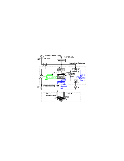
Figure 1 shows the complete schematic diagram of the detection system, consisting of the pulse handling part, the microwave PLL, and the amplitude readout part, together with the CPW sample in a cryogenic environment. The main microwave components of this system are basically a pair of homodyne mixers (M1 and M2) with different reference signals of quadrature phase difference generated by a 90° hybrid (H). The signal from the sample is divided equally into two part by a power divider (D). The mixer M1 with a 0° reference (LO1), used as the phase sensitive detector (PSD), has zero output (IF1) forced by the PLL, and at the same time the other mixer M2 with a 90° reference (LO2) has an output (IF2) proportional to the amplitude of the signal.

To reduce the signal power level and increase the signal to noise ratio, besides homodyne detection we also employ a double-pulse modulation scheme to detect and average the microwave signal. Figure 2 shows the sequence of the controlling pulses and some other related outputs. A short pulse train [GP in Fig. 2(b)] with a 0.22 s pulse width and a 0.110% duty cycle, provided by a pulse generator (PG in Fig.1) and gated by a slow square-wave TTL signal (TTL1) shown in Fig. 2(a) with a period of 110 ms from a lock-in amplifier, modulates the microwave signal sent to the sample. A time-delayed pulse (SP) with a 0.21 s pulse width, triggered by the modulating pulses, controls a sample-and-hold (S&H) circuit that samples the IF output (IFO) of the microwave mixer. The output of the S&H circuit (SHO) is set to zero by an analog switch when the TTL gating signal is low. The output of the S&H circuit has the same characteristic frequency as the signal TTL1, and hence can be averaged and read out by the lock-in amplifier.
We use two sets of pulse averaging circuits in this system, one for the PLL part and the other for the amplitude detection part. Even though the lock-in amplifiers therein are synchronized at the same operating frequency, their averaging time constants are different. The time constant of LOCKIN1 in the PLL is about 110 ms for fast loop dynamics, in contrast to 300 ms or 1 s of LOCKIN2 in the amplitude readout part for low average noise. The average of the PSD output (IF1) is then sent to an integrator (loop filter of PLL), whose output is connected to the frequency modulation (FM) input of the microwave source (SG), i.e. the VCO of the PLL, and thus the loop is closed.
II.3 Pulse Handling Circuits and the Integrator
The short pulse trains used in this system are provided by a simple single-channel pulse generator TPG110 from TTiTTi , which can generate a short reference pulse train (SYN in Fig. 2) and a pulse train (SP) with tunable time delay (relative to SYN), pulse width, and duty cycle, and a homemade pulse shaping circuit (Fig. 3), which converts the 30-ns-width reference pulses (SYN) to the gating pulses (GP) with 0.22 s pulse width that are sent to a diode switch (S) to modulate the microwave signal. A lock-in amplifier (LOCKIN1), SR830 from SRS,lockin sends a slow TTL square-wave reference (TTL1) to the ”trigger/gate in” input of TPG110. Another lock-in amplifier (LOCKIN2) is externally locked to LOCKIN1 and used to read the IF output of M2 (IF2).

The simple pulse shaping circuit in Fig. 3 consists of a BJT switch (2N3904), a CMOS and a TTL invertors. During the 30-ns duration given by SYN pulses, 2N3904 is turned on and allows certain amount of charge (set by R2 and R3) to flow into C1 and the TTL output (GP) will be set to high from low. Afterwards the voltage across C1 (VC1) drops below 2.5 V due to the discharging current through R1 (in series with a 1 k resistor), that triggering the following invertors to switch their statuses and thus making the output (GP) back to low. The width of the output pulse can be tuned via the variable resistor R1, and the tunable range of the pulse width can be adjusted by R2 and R3.
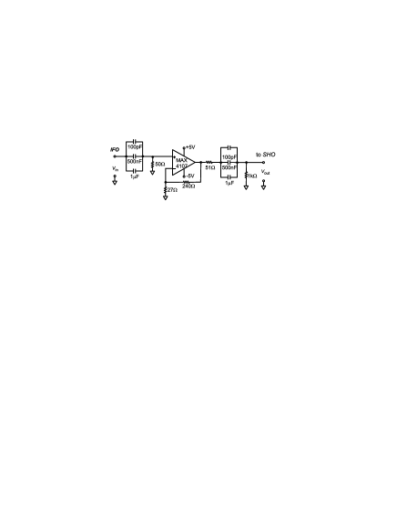
Each IF output of the mixers (M1 and M2) is low-pass filtered and then amplified by a pulse amplifier before fed into the sample-and-hold circuit. The low-pass filters used here are PLP-5 (5MHz) or PLP-70 (70MHz) from Mini-Circuits,minicircuits depending on the pulse width of the gating pulse (GP). For the pulse amplifier, we use a high-speed low-noise operational amplifier MAX4107maxim connected in a non-inverted configuration as shown in Fig. 4. Its rise/fall time is well below 10 ns for a typical pulse height (1 V) in our application.

The sample-and-hold circuit is shown in Fig. 5. We use a high-speed sample-and-hold amplifier IC HA-5320-5,intersil which provides a 100 ns rise time and a 25 ns aperture time, and a fast analog switch ADG201HSADI followed by a buffer BUF04ADI . The main output of TPG110 (SP) is connected to the S/H control (lead 14) of HA-5320-5, and the slow reference TTL1 from LOCKIN1 controls ADG201HS and makes the output SHO zero as TTL1 goes low.discharge
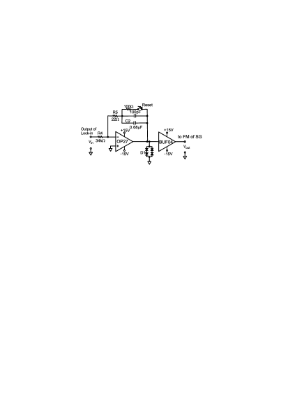
A simple integrator shown in Fig. 6 serves as the loop filter of the PLL. The integration time constant () is about 23 ms, which is chosen to be higher then the time constant of LOCKIN1 such that the dynamics of the PLL is mainly controlled by this integrator. Two sets of series-connected diodes (D1) are connected in parallel from the output of the integrator to the ground with inverted polarities and used as a voltage limiter to protect the FM input of the microwave generator (SG). A manual switch is used to reset the integrator while the PLL is saturated or unlocked. R5 gives the PLL an adequate damping that may attenuate unwanted oscillations in the loop. The dynamic properties of this PLL system will be discussed later in Sec. III.
II.4 Microwave Modules
We use several sets of microwave modules to cover the frequency range from about 100 MHz to 18 GHz. Table I lists the model numbers of the modules (including the vendors in the footnotesvendors ) according to their operation band. Please note that the amplifers (A) includes a front-end low-noise preamplifier (LNA) and subsequent amplifiers to make the total gain about 60 dB. To cover the whole band, we use two LNAs with noise figure (NF) better then 1.4 dB and 2.2 dB for frequency range 0.18 GHz and 618 GHz, respectively. The microwave signal source (SG) used here is model E4421B (250k-3GHz) or E8254A (250k-40GHz) from Agilent,vendors both with FM bandwidth down to DC.
|
Diode Switch (S) |
|
90° Hybrid (H) | Divider (O) | LNA + Amp (A) |
|
||||||||
|---|---|---|---|---|---|---|---|---|---|---|---|---|---|---|
|
ZASWA-2-50DRa | ZFM-2000a |
|
ZFSC-2-2500a |
|
|
||||||||
| 2-4.3 | ZASWA-2-50DRa | ZEM-4300a | QS4-01-464/3c | ZFSC-2-10Ga |
|
|
||||||||
|
N138BDF1b | DB0218LW2b | QS2-07-464/4c | 2089-6209-00d |
|
|
a Mini-circuits; b MITEQ; c Quinstar; d M/A COM; e Pulsar Microwave; f Agilent.
III Results and Discussions
III.1 Response of the PLL
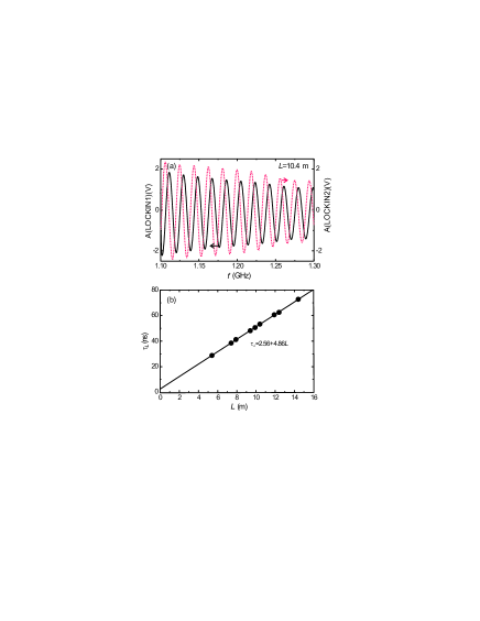
The response of this PLL system is mainly controlled by four parameters, the power of the signal from the sample back to the LNA, the sensitivity of LOCKIN1 (), the FM deviation per volt (, with unit Hz/V) of the VCO, and the total length of the semirigid coaxial cables, all of which can be tuned by the instrumental setting in our design. The length of the semirigid cables affects the delay time in Eq. 1. We can measure precisely with this PLL system itself without using an additional conventional VNA or time domain reflectometer (TDR). In the unlock condition, i.e. with FM off in SG (VCO), we recorded the output of LOCKIN1 (or LOCKIN2) as a function of frequency , and the result can be expressed as with the oscillation amplitude, and a relative phase factor. Figure 7(a) shows the oscillations for both LOCKIN1 and LOCKIN2 near = 1.2 GHz with only a 10.4-m semirigid cable and no sample connected to the PLL system between the attenuator (AT) and A in Fig.1. As expected, the oscillations of these two channels are 90° out of phase due to the LO phase difference of two mixers. From the “frequency” of these oscillations, we can directly estimate to be 53.3 ns. Figure 7(b) shows that is a linear function of the length of the semirigid cable with a finite intercept, about 2.6 ns, on the vertical axis. This extra delay time corresponding to a zero-length cable can be attributed to the time delay in the microwave modules. The peak power of the microwave signals used in these tests is -70 dBm.
The phase change of the CPW device in the experiment is the product of the output of the integrator in the PLL, and while keeping the PLL in the locked condition. is in fact the change in the frequency () of the VCO, which can also be measured by a microwave counter. of the signal source may affect the phase resolution: the smaller is the FM deviation set, the higher is the phase sensitivity. However, if is set too small, the PLL may saturate very easily (the output of the integrator reaches or V), and the phase signal readout is also very noisy. Usually needs to be set properly according to the dynamic range of the phase signal.
For low-temperature experiments, usually the signal power to the sample is set by a step attenuator and is chosen to be the highest value without any heating effect on the sample. For samples immersed in liquid He3 at 0.3 K, typically a peak power of -50 dBm microwave signal, equivalent to an average power of -65 to -80 dBm depending on the duty cycle of the modulating pulses, can be delivered to the sample without raising the sample temperature.
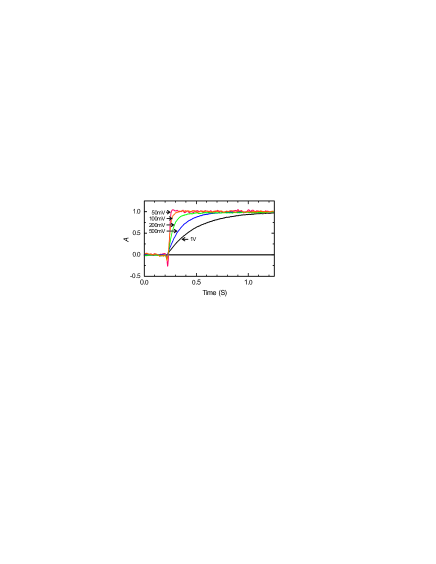
The response time of the PLL is affected by the total gain of the loop, which can be obtained from the amplitude of the oscillations in Fig. 7(a) and . can be easily controlled by of LOCKIN1, and this provides a very convenient method to control the response time of the PLL during the experiment. Figure 8 shows the step response for different value of . In this test, we also used a 10.4-m semirigid cable without sample attached to the PLL system. was set at 1 MHz/V, the peak power of the microwave signal after the attenuator was -70 dBm, and the operation frequency was about 1.2 GHz. The step response was measured from the output of the integrator as function of time right before we increased the unmodulated frequency of SG by a step of 500 kHz while the PLL was kept in a locked condition. The rise time of the response can be tuned from 0.63 s for V to 0.015 s for mV, and at the same time the loop dynamic behavior is moved from an overdamped regime to a slightly underdamped regime. We also find that the fluctuation of the signal decreases as increases. There is apparently a tradeoff between the speed of the loop and the signal fluctuation.
III.2 Detection Limit
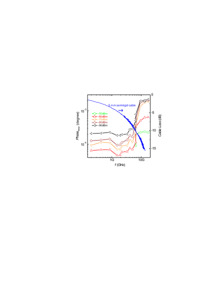
To gain an idea of the detection limit of this system, we measured the background noise in the phase signal with only a 5.4-m semirigid cable attached to the system. Various microwave modules were used to cover the whole available frequency range. Figure 9 shows the measured peak-to-peak phase fluctuation versus frequency for different peak power levels of the microwave signal after the step attenuator (AT) together with the loss of the semirigid cable measured by a VNA. The phase signal was read from and then multiplied by . The measured bandwidth is controlled by the time constant of the integrator (23 ms), equivalent to about 7 Hz. was fixed at 500 mV and was set at 50 kHz/V during this test. The modulating pulses had a 2 s pulse width and a 1/75 duty cycle. The gating window of the S&H circuit was 350 ns.
The collected data shown in Fig. 9 indicate that below 5 GHz, even for the lowest peak power -90 dBm in our test, the phase fluctuation is still less than 0.0003°; above 5 GHz to 18 GHz, the fluctuation is still controlled within about 0.002°. This noise level is remarkably low for such a low-power signal. Here we want to note that to obtain the average power value we must further subtract about -21.8 dBm from the peak power value due to the low duty cycle. In fact, the signal power reaching the low-noise amplifier (LNA) is even lower than the input value claimed above due to the loss of the cable as also shown in Fig. 9. This may explain the noise in phase increases at high frequencies. The resolution with a low- sample loaded is slightly worse due to the loss of the sample and extra noise from the cryogenic environment. The resolution of the amplitude readout for a small-variation signal can be enhanced by the use of the ”offset” and ”expand” functions of the lock-in amplifier.lockin
III.3 Applications to Low-Dimensional Electron Systems
In the following we will present measured results for a 2DES sample (sample A) and a QW array sample (sample B) to demonstrate the capability of this system. The 2DES in the sample A is confined in a 20-nm-wide modulation-doped In0.15Ga0.85As quantum well grown on GaAs substrate by molecular beam epitaxy (MBE) technique. The quantum well is separated from a 260 nm Al0.3GaAs Si-doped layer by a 15-nm GaAs and a 5nm Al0.3GaAs undoped spacer layers. This 2DES has an electron density of cm-2 and a mobility of about cmV s at 0.3 K. A 50- () meandering CPW made of Au(300 nm)/Ti(10 nm) with a 36 m wide central conductor and a 23 m gap () between the central conductor and the ground plane at both sides is manufactured on the surface of the substrate. The effective length of the meandering CPW is 2.25 cm. The sample is immersed in liquid 3He (0.3 K) with applied perpendicular to the sample surface. The real part and the imaginary part of the longitudinal conductivity can be deduced from the relative amplitude changeEngel1993 of the microwave signal () and the phase differenceSuen2002 obtained from Eq. 1, respectively, via
| (2) |
and
| (3) |
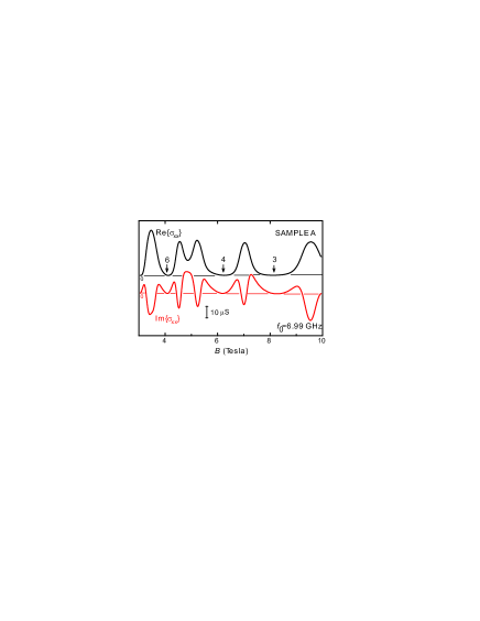
Figure 10 shows the Re and Im of the sample A at 6.99 GHz for between 3 and 10 T. The scale bar on the plot is 10 S for both curves. The peak power into the sample was about -85 dBm, and the equivalence average power was only about -105 dBm. The Re curve shows clear broad minima near zero conductance around integer Landau level filling factors (), while the Im curve exhibits a concave shape in the plateau regime and a deep minimum in the transition region between adjacent Hall states. This observation is very similar to what Hohls et al.Hohls2001 reported; however, compared to their presented data (Fig. 2 in Ref. 9), our data give a much less background noise than theirs. The background fluctuation for both curves in Fig. 10 is only about 50 nS.
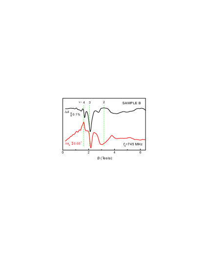
The sample B is fabricated from a typical MBE-grown modulation-doped GaAs/AlGaAs heterostructure containing a 2DES, which is 150 nm under the surface. The mobility of the 2DES is 1.6 cmVs at 4K, and the density is 1.02 cm-2. The 2DES under the CPW pattern was first removed by chemical etching before the metal-film deposition. The 2DES left in the gap was then patterned into about 7000 identical QW mesas, each of 0.7 m wide and 20 m long, by using e-beam lithography and chemical etching. Other experimental details can be found in our previous publication.Hsieh2004 Figure 11 shows a typical data, including both the amplitude change and the phase variation as a function of . The peak power of the pulsed microwave signals used in this measurement was 50 dBm (about 66 dBm in average) before fed into the sample. The amplitude and phase fluctuations in and data are less than 0.003% and 0.001°, respectively. The Landau level filling factor () is assigned according to the electron density in each QW from the Shubnikov-de-Haas oscillations observed in high-frequency data.Hsieh2004
In summary, we have developed and demonstrated a high-sensitivity vector detection system for very low-power microwave signals used in a CPW broadband sensor. This system is a very powerful tool in studying the dynamic behaviors of LDESs at low temperatures.
Acknowledgements
This work was supported by the National Science Council of the Republic of China under Contract No. NSC93-2112-M005-009.
References
- (1) L. W. Engel, D. Shahar, C. Kurdak, and D. C. Tsui, Phys. Rev. Lett. 71, 2638 (1993).
- (2) C.-C. Li, L. W. Engel, D. Shahar, D. C. Tsui, and M. Shayegan, Phys. Rev. Lett. 79, 1353 (1997).
- (3) P. D. Ye, L. W. Engel, D. C. Tsui, R. M. Lewis, L. N. Pfeiffer, and K. West, Phys. Rev. Lett. 89, 176802 (2002).
- (4) R. M. Lewis, P. D. Ye, L. W. Engel, D. C. Tsui, L. N. Pfeiffer, and K. W. West, Phys. Rev. Lett. 89, 136804 (2002).
- (5) Y. Chen, R. M. Lewis, L. W. Engel, D. C. Tsui, P. D. Ye, L. N. Pfeiffer, and K. W. West, Phys. Rev. Lett. 91, 016801 (2003).
- (6) I. Grodnensky, D. Heitmann, K. v. Klitzing, K. Ploog, A. Rudenko, and A. Kamaev, Phys. Rev. B 49, 10778 (1994).
- (7) P. D. Ye, L. W. Engel, D. C. Tsui, J. A. Simmons, J. R. Wendt, G. A. Vawter, and J. L. Reno, Phys. Rev. B 65, 121305 (2002).
- (8) R. M. Lewis and J. P. Carini, Phys. Rev. B 64, 073310(2001).
- (9) F. Hohls, U. Zeitler, and R. J. Haug, Phys. Rev. Lett. 86, 5124 (2001).
- (10) W. H. Hsieh, Y. W. Suen, S. Y. Chang, L. C. Li, C. H. Kuan, B. C. Lee, and C. P. Lee, Appl. Phys. Lett. 85, 4196 (2004).
- (11) R. White, Spectrum and Network Measurements (PTR Prentice Hall, New Jersey, 1993).
- (12) For the design of PLLs, please see, e.g., Roland E. Best, Phase-Locked Loops, 5th ed. (McGraw-Hill, Inc., 2003).
- (13) A. Wixforth, J. Scriba, M. Wassermeier, J. P. Kotthaus, G. Weimann, and W. Schlapp, Phys. Rev. B 40, 7874 (1989).
- (14) Thurlby Thandar Instruments Ltd., Huntingdon, Cambridgeshire PE29 7DR, U.K.
- (15) SR830 from Stanford Research Systems, Inc., Sunnyvale, CA.
- (16) Mini-Circuits, Brooklyn, NY.
- (17) Maxim Integrated Products, Sunnyvale, CA.
- (18) Intersil Corporation, Milpitas, CA.
- (19) Analog Devices, Inc., Norwood, MA.
- (20) In this design, we need to insert a TTL invertor between the TTL1 and the control lead of the analog switch since there is a built-in invertor between input and the switch control in ADG201HS.
- (21) MITEQ, Hauppauge, NY; Quinstar Technology Inc., Torrance, CA; M/A COM, Lowell, MA; Pulsar Microwave Corp., Clifton, NJ; Agilent, Palo Alto, CA.
- (22) Y. W. Suen, W. H. Hsieh, L. C. Li, T. C. Wan, C. H. Kuan, S. D. Lin, C. P. Lee, and H. H. Cheng, Proc. of the 15th Intl. Conf. on High Magnetic Field in Semiconductor Phys., Oxford, U.K., B48 (2002).