Strain control of superlattice implies weak charge-lattice coupling in La0.5Ca0.5MnO3
Abstract
We have recently argued that manganites do not possess stripes of charge order, implying that the electron-lattice coupling is weak [Phys Rev Lett 94 (2005) 097202]. Here we independently argue the same conclusion based on transmission electron microscopy measurements of a nanopatterned epitaxial film of La0.5Ca0.5MnO3. In strain relaxed regions, the superlattice period is modified by 2-3% with respect to the parent lattice, suggesting that the two are not strongly tied.
pacs:
75.47.Lx 71.38.-k 71.45.Lr 61.14.LjThe superlattice present in many manganites has traditionally been described in terms of a charge ordered array of the idealised cations Mn3+ and Mn4+ J.P. Goodenough (1955); E.O. Wollan, W.C. Koehler (1955); C.H. Chen, S.-W. Cheong (1996); N.D. Mathur, P.B. Littlewood (2001). This superlattice is observed in x-ray, neutron and electron diffraction patterns as extra reflections that typically lie along or near a∗, indexing the room temperature cell as orthorhombic . Recent work controversially suggests that Mn valence charges are not strongly localised, and that any charge modulation is very small J. García et al. (2001); J. Rodríguez-Carvajal et al. (2002); V. Ferrari, M.D. Towler, P.B. Littlewood (2004); J.C. Loudon et al. (2005a); L. Brey (2004); E.E. Rodriguez et al. (2005).
We recently argued that in polycrystalline La1-xCaxMnO3 () at 90 K, the charge-lattice coupling is weak because the superlattice is not locked to the parent lattice J.C. Loudon et al. (2005a). Instead, the periodicity of the superlattice was found to be uniform over a wide range of length scales in any particular grain. Our main evidence was that the superlattice wavenumber was invariant with respect to when a grain was repeatedly sampled with a local probe (convergent beam electron diffraction, spot size 3.6 nm). This interpretation relied upon selecting x=0.52 such that C.H. Chen, S. Mori, S.-W. Cheong (1999) was near but not equal to 0.5. In bulk unstrained La0.5Ca0.5MnO3, below the Néel transition temperature K (on cooling) C.H. Chen, S.-W. Cheong (1996). The superstructure persists up to the Curie temperature of K, and for , is hysteretic and incommensurate C.H. Chen, S.-W. Cheong (1996).
It has previously been suggested that the superlattice of a manganite should be modified by strain N.D. Mathur, P.B. Littlewood (2001). Intergranular variations in of up to 8% have been observed in polycrystalline La0.5Ca0.5MnO3 J.C. Loudon et al. (2005b), but the possibility of extrinsic effects precludes a direct link with strain. Here we investigate tuning the strain state in a continuous crystal lattice, where extrinsic effects should be minimised. Although chemical phase separation prevents the growth of bulk single crystal La1-xCaxMnO3 ( P. Majewski et al. (2000), we have formed an untwinned continuous crystal lattice by growing a coherently strained epitaxial film of La0.5Ca0.5MnO3 on an orthorhombic NdGaO3 (001) substrate (NGO). Superlattice reflections are expected to be strongest at this composition, since optical spectroscopy measurements show a “pseudogap” in La1-xCaxMnO3 that is largest at K.H. Kim et al. (2002). We have attempted to release the epitaxial strain in some areas of the film by firstly removing substrate material to create an electron transparent window 150 nm thick, and then removing material around rectangular micron-scale regions (“rectangles”) within the window. Transmission electron microscopy (TEM) revealed that is reduced by 2-3% inside the rectangle.
Films were grown at 800∘C in a flowing oxygen ambient of 15 Pa by pulsed laser deposition from a polycrystalline La0.5Ca0.5MnO3 target (Praxair, USA) using a 248 nm ultraviolet KrF laser with an average fluence of 1.5 J.cm-2, a repetition rate of 1 Hz and a target-substrate distance of 8 cm. Films were subsequently annealed for one hour in 60 kPa O2 at 800oC. The lattice parameter of NGO at the 90 K nominal base temperature of our microscope stage is 0.48% smaller than the lattice parameter of La0.5Ca0.5MnO3, and the mismatch in is 0.35% in the opposite sense D. Savytskii et al. (2003). The film was nm thick as measured by high resolution X-ray diffraction (HRXRD). This thickness is sufficiently low to preserve cube-on-cube epitaxy. An X-ray rocking curve with a FWHM of 0.10∘ for the (004) film reflection was recorded, and a typical value for surface roughness as measured by atomic force microscopy was 0.5 nm. A ferromagnetic signal detected below room temperature reached an apparent saturation magnetization of 0.6 /Mn at 90 K, with no evidence for the antiferromagnetic transition that is observed in the bulk above 100 K P.E. Schiffer, A.P. Ramirez, W. Bao, S.-W.Cheong (1995). Similarly, no transitions were seen in the electrical resistivity, which was 0.02 .cm at 300 K and remained insulating down to 80 K, beyond which we could no longer measure it.
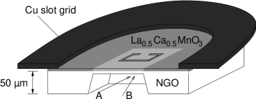
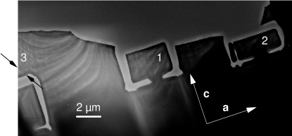
The sample was prepared for TEM by conventional grinding to 50 m, and processing using the focussed ion beam (FIB) microscope (Fig. 1). The electron transparent window was defined by cutting substrate material from under the film. When the window was m thick, the sample was tilted 45∘ and cuts were made from the substrate side to minimise film damage. These cuts defined a free standing rectangular region (a “rectangle”). The sample was then rotated back to its original position with sufficient precision to avoid an undercut during subsequent thinning of the window to electron transparency. Material furthest from the front edge of the window in Fig. 1 was therefore thickest. A low magnification TEM picture of two rectangles is shown in Fig. 2. The minimum thickness of the window that could be achieved reliably was 150 nm. Thus 100 nm of substrate remained attached to the 44 nm film.
The sample was cooled to approximately 90 K for up to four hours at a time using a Gatan double-tilt liquid nitrogen stage. Parent lattice reflections were recorded in diffraction patterns with a CCD camera on a Philips CM300 TEM operated at 300 kV. However, superlattice reflections were too weak to measure on the CCD without significant over-saturation of the parent reflections. Therefore measurements of were extracted from diffraction patterns recorded on photographic film, which has a sensitive nonlinear response. For this a Philips CM30 TEM operated at 300 kV was used with a 500 nm aperture.
At 90 K all regions of the electron transparent window (both inside and outside the rectangles) produced diffraction patterns showing the superlattice. As expected, the superlattice modulations were always parallel or near-parallel to the a∗ direction. Custom written software was used in order to measure statistically significant values of for each diffraction pattern. Initially the parent lattice reflections were identified and the distortion of the photographic film was calculated, then the positions of the superlattice reflections were found. Thus values of were established for each diffraction pattern.
Specifically, the positions of the parent lattice reflections were estimated and then refined using the mean-shift algorithm. The film distortion was calculated using the projective warp which models the distortion as shear, aspect ratio change and keystoning.
Pairs of superlattice reflections that appeared between adjacent pairs of parent lattice reflections along the a∗ axis were modelled using the weighted sum of two Gaussians and a constant value. The parameters were fitted to this Gaussian Mixture Model (GMM) using the Expectation Maximisation algorithm A. Dempster, N. Laird, D. Rubin (1977); R.A. Redner, H.F. Walker (1984). Information was ignored from areas near the edge of the photographic film that were warped such that the mismatch between the expected lattice and the observed lattice was greater than two pixels. The curvature of the Ewald sphere leads to a systematic error , where is the measured value of the wavevector and is the wavevector measured across the Ewald sphere, but this is small and will affect equally both the parent and superlattice reflections, such that it may be ignored here.
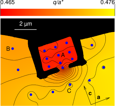
Fig. 3 shows a map of in and around Rectangle 1. The magnitude of was highest at C, 0.8% lower at B, and 1.4% lower again inside the rectangle at A (0.47600.0009, 0.47100.0005 and 0.46460.0006, respectively). Similarly, for Rectangle 2, at points analogous to B and A differ in the same sense by 1.3% (0.47530.0005 and 0.46920.0007 respectively). In any given diffraction pattern, each individual measurement of was recorded to within 0.004, given a resolution of 0.3 out of 35 pixels. For each diffraction pattern, between 150 and 300 measurements of were made, reducing this error to the values quoted.
At any point in the window, the measured wavenumber varied between cooling runs. The range of inside Rectangle 1 at point A was 2.6% (0.457 – 0.469). Outside Rectangle 1 at point C, the range was 1.9% (0.467 – 0.476). However, in any given run, the wavenumber outside the rectangle was always larger than the wavenumber inside the rectangle, with the run to run difference from A to C being between 2.2% – 3.2%.
Since rather than is measured, we investigated whether the observed variations of a few could be due to variations in alone. The parent lattice reflections were recorded in different areas of the sample above and below the ordering transition temperature of 220 K as estimated from polycrystalline samples C.H. Chen, S.-W. Cheong (1996). Variations in were , which assuming to be constant implies that variations in . This places an upper bound of 0.1% on changes in due to unresolved changes in . (Note that this error calculation is non-trivial because the measured is always determined relative to the measured .) Therefore the spatial variations seen in represent changes in , whether or not they are driven by changes in that are beyond the 1% resolution of the microscope.
The asymmetry in with respect to the artificial cuts rules out the possibility that contamination and/or damage from the Ga beam of the FIB microscope produce the observed changes in our measurements taken at points over 500nm from the artificial edges. Moreover, when moving from 4 m to within 1 m of a natural crack (Fig. 2), was reduced by 1.3% (0.476 to 0.470). This mimics the change in that we engineered in the rectangle.
The observed differences between inside and outside the rectangle could be due to the electron beam heating the rectangle, which is thermally isolated by its small neck. However, one would then expect to vary in a systematic way with remoteness from the neck. This is not the case so thermal effects cannot explain the results of this experiment.
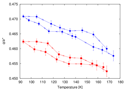
The observed reduction of inside the rectangle could also arise if discommensurations, which separate regions of different , were pinned strongly inside the rectangle, due to defects at the nearby edges, and could not propagate through the neck. Temperature sweeps taken inside and outside the rectangle both show a similar hysteresis of 20 K (Fig. 4). This suggests that the degree of pinning is similar inside and outside the rectangle, and that pinning does not cause the observed differences in .
We suggest that small changes in strain, below our resolution in , are responsible for the observed variations in . Indeed, changes this small can be significant. For example, a 0.5% change of strain Y.-A. Soh et al. (2002) along the normal to the surface of a La0.7Sr0.3MnO3 Y.-A. Soh et al. (2001) film produces a 20 K change in the Curie temperature.
Our observation that is smallest inside the rectangle may be understood using a 1D Ginzburg-Landau theory P. Bak, J. Timonen (1978). In the modulated manganite we studied, the nature of the order parameter is not established J.C. Loudon et al. (2005a). Here we express it in terms of the corresponding order parameter in the absence of modulations as where r is the spatial coordinate, is a vector commensurate with the lattice and incorporates incommensurability G.C. Milward, M.J. Calderón, P.B. Littlewood (2005). The wavevector is given by , where is the deviation of the wavevector from the commensurate value. Therefore in our material . Assuming that is constant, we can write the free energy density for the modulation and its coupling with strain as P. Bak, J. Timonen (1978)
| (1) |
The first term is the elastic term that favours incommensurate modulation, and we arbitrarily set =1. The parameter is the deviation of from 0.5 in the absence of strain coupling. We always see in our film, which we suggest is due to the presence of a background strain that arises from our inability to completely remove strain everywhere, in effect rendering . The second term is the Umklapp term that favours commensurability, where is an integer and the coefficient determines the strength of the effect. The third term couples and with strength . The fourth term is the strain energy density in terms of the bulk elastic modulus . The fifth term gives the elastic energy due to the stress on the film from the substrate. The effect of the coupling term on the wavevector can be determined in the plane-wave limit (constant and ) by minimising (1), which leads to
| (2) |
Two limiting cases represent the situation inside and outside the rectangle respectively: either the film relaxes in the absence of substrate-induced stress and is reduced by to give , or the film is clamped such that the coupling is inactive, and thus and . Since we can understand why the deviation from the commensurate value of will be larger inside a rectangle whatever the sign of . Note that this result is the opposite of what might be expected given that the rectangle resembles an unstrained single crystal.
We now consider whether the changes in , that we ascribe to strain, support our recent finding that the charge-lattice coupling is weak J.C. Loudon et al. (2005a). In the traditional strong-coupling limit, any elastic deformation of the parent lattice should be directly transmitted to the superlattice such that =0. Our finding that =2-3% suggests that the superlattice can deform independently of the parent lattice. Therefore the coupling cannot be considered arbitrarily strong. Moreover, in the traditional strong-coupling picture, the changes in that we observe would arise due to changes in the number of [100] Mn4+ sheets, and these are not available at a given . In theory, our finding that could be explained if strain is enhanced at uncharged discommensurations P. Bak, J. Timonen (1978), but discommensurations are not consistent with a strong coupling picture at x=0.5.
In summary, we have shown that it is possible to tune the magnitude of by up to 3% in La0.5Ca0.5MnO3 at 90 K by processing a thin film using an FIB microscope. This demonstrates that tuning the microstructure of La0.5Ca0.5MnO3 can alter the low temperature superlattice. Consequently the variations in wavenumber seen in polycrystalline La1-xCaxMnO3 J.C. Loudon et al. (2005a); J.C. Loudon et al. (2005b) may be directly attributed to strain. Our finding that may be most simply explained if the charge and lattice are weakly coupled. The interpretation presented here supports our earlier suggestion J.C. Loudon et al. (2005a) that a charge density wave scenario may be appropriate.
Acknowledgements.
We thank M.B. Weissman and L.E. Hueso for helpful comments. This work was funded by the UK EPSRC, The Royal Society, the Schiff Foundation, and Churchill College, Cambridge.References
- J.P. Goodenough (1955) J.P.Goodenough, Phys. Rev. 100, 564 (1955).
- E.O. Wollan, W.C. Koehler (1955) E.O. Wollan, W.C. Koehler, Phys. Rev. 100, 1 (1955).
- C.H. Chen, S.-W. Cheong (1996) C.H. Chen, S.-W. Cheong, Phys. Rev. Lett. 76, 4042 (1996).
- N.D. Mathur, P.B. Littlewood (2001) N.D. Mathur, P.B. Littlewood, Solid State Commun. 119, 271 (2001).
- J. García et al. (2001) J. García et al., J. Phys.-Condens. Mat. 13, 3243 (2001).
- J. Rodríguez-Carvajal et al. (2002) J. Rodríguez-Carvajal et al., Physica B 320, 1 (2002).
- V. Ferrari, M.D. Towler, P.B. Littlewood (2004) V. Ferrari, M.D. Towler, P.B. Littlewood, Phys. Rev. Lett. 91, 227202 (2004).
- J.C. Loudon et al. (2005a) J.C. Loudon et al., Phys. Rev. Lett. 94, 097202 (2005a).
- L. Brey (2004) L. Brey, Phys. Rev. Lett. 92, 127202 (2004).
- E.E. Rodriguez et al. (2005) E.E. Rodriguez et al., Phys. Rev. B 71, 104430 (2005).
- C.H. Chen, S. Mori, S.-W. Cheong (1999) C.H. Chen, S. Mori, S.-W. Cheong, J. Phys. IV France 9, Pr10-307 (1999).
- J.C. Loudon et al. (2005b) J.C. Loudon et al., Phil. Mag. 85, 999 (2005b).
- P. Majewski et al. (2000) P. Majewski et al., J. Mater. Res. 15, 1161 (2000).
- K.H. Kim et al. (2002) K.H. Kim et al., Phys. Rev. Lett. 88, 167204 (2002).
- D. Savytskii et al. (2003) D. Savytskii et al., Phys. Rev. B 68, 024101 (2003).
- P.E. Schiffer, A.P. Ramirez, W. Bao, S.-W.Cheong (1995) P.E. Schiffer, A.P. Ramirez, W. Bao, S.-W.Cheong, Phys. Rev. Lett. 75, 3336 (1995).
- A. Dempster, N. Laird, D. Rubin (1977) A. Dempster, N. Laird, D. Rubin, J. Roy. Stat. Soc. B 39, 1 (1977).
- R.A. Redner, H.F. Walker (1984) R.A. Redner, H.F. Walker, SIAM Review 26, 195 (1984).
- Y.-A. Soh et al. (2002) Y.-A. Soh et al., J. Appl. Phys. 91, 7742 (2022).
- Y.-A. Soh et al. (2001) Y.-A. Soh et al., Phys. Rev. B 63, 020402 (2001).
- P. Bak, J. Timonen (1978) P. Bak, J. Timonen, J. Phys. C Sol. State Phys. 11, 4901 (1978).
- G.C. Milward, M.J. Calderón, P.B. Littlewood (2005) G.C. Milward, M.J. Calderón, P.B. Littlewood, Nature 433, 607 (2005).