Stoichiometry control of magnetron sputtered Bi2Sr2Ca1-xYxCu2Oy (0x0.5) thin film, composition spread libraries: Substrate bias and gas density factors.
Abstract
A magnetron sputtering method for the production of thin-film libraries with a spatially varying composition, x, in Bi2Sr2Ca1-xYxCu2Oy (0x0.5) has been developed. Two targets with a composition of Bi2Sr2YCu2O8.5+δ and Bi2Sr2CaCu2O8+δ are co-sputtered with appropriate masks. The target masks produce a linear variation in opposite, but co-linear radial direction, and the rotation speed of the substrate table is sufficient to intimately mix the atoms. EDS/WDS composition studies of the films show a depletion of Sr and Bi that is due to oxygen anion resputtering. The depletion is most pronounced at the centre of the film (i.e. on-axis with the target) and falls off symmetrically to either side of the 75 mm substrate. At either edge of the film the stoichiometry matches the desired ratios. Using a 12 mTorr process gas of argon and oxygen in a 2:1 ratio, the strontium depletion is corrected. The bismuth depletion is eliminated by employing a rotating carbon brush apparatus which supplies a -20 V DC bias to the sample substrate. The negative substrate bias has been used successfully with an increased chamber pressure to eliminate the resputtering effect across the film. The result is a thin film composition spread library with the desired stoichiometry.
keywords:
High-Tc films , Bi-based cuprates , Cuprate superconductors (high-Tc and insulating parent compound) , Composition spread libraries , Magnetron sputtering , Stoichiometry , Resputtering , Substrate bias.PACS:
74.72.-h , 74.72.Hs , 74.78.Bzurl]http://fizz.phys.dal.ca/ hewitt
1 Introduction
It is widely accepted that oxygen has to be added to the sputtering gas for the deposition of Bi2Sr2CaCu2O8+δ (Bi-Ca-2212) thin films [1, 2, 3, 4]. The drawback to using oxygen in the sputtering gas is a pronounced resputtering of the deposited film, as found in Bi-Ca-2212 [5, 6] and YBa2Cu3O7-δ [7, 8, 9, 10, 11] superconducting systems. Oxygen anions derived from the sputtering gas and target material are the source of this resputtering effect [12]. The anion is accelerated away from the negatively charged target, and if the energy is large enough, it will escape the magnetron’s magnetic field. The energetic anions sputter the deposited film, in a manner than preferentially depletes atoms with large scattering cross section. This resputtering effect produces the undesirable effect of changing the composition of the film relative to the target.
There have been several reported methods to reduce the resputtering phenomenon in these materials. The most common approach is to use an off-axis deposition method, where the substrate is not directly across from the target. Rather, the substrate is placed at an angle 90o relative to the axis of the cylindrical target. It has been found that the energy of oxygen anions that strike the film is reduced [1, 5, 6, 7, 8, 9, 10, 11]. Off-axis sputtering greatly reduces the deposition rate, which is not desirable. To further reduce resputtering, it has been shown that increasing the sputtering gas pressure can increase the anion-gas collisions, reducing their energy or deflecting them away from the film. Increasing the gas pressure usually reduces the target bias. The energy of the anions is thereby decreased; however, the increased gas pressure also decreases the film deposition rate due to target atom-gas collisions. A third method to compensate for resputtering is to alter the target stoichiometry to account for the non-uniform depletion of elements [5, 7, 9]; this is sometimes not possible as the required target composition may not be an equilibrium phase. A final method uses a negative bias shield or substrate bias to deflect the anions away from the deposited film [1, 3].
Physical vapor deposition has been used since 1965 to explore phase diagrams using a composition-spread approach [13, 14, 15, 16, 17, 18]. In this technique, a large range of compositions is deposited on a single substrate in a single deposition run. Our group has established a composition spread approach which uses magnetron sputtering to prepare a continuous variation of composition across a 75 mm substrate [19].
Therefore, to develop a magnetron sputtering method for the production of cuprate superconductor thin-film samples with a spatially varying composition, x, in Bi2Sr2Ca1-xYxCu2Oy (0x0.5), resputtering effects have to be addressed as it has a detrimental effect on the composition of the deposited film. An apparatus had to be designed to bias the substrates while affixed to a rotating substrate table. The novel aspect of this paper is the introduction of a rotation-compatible substrate bias apparatus that uses an existing magnetron to supply a constant -20 V bias to the substrates in order to prepare a cuprate superconductor composition spread library.
2 Experiment and Results
The composition spread approach uses simultaneous, magnetron sputtering of two targets, e.g. A and B. Masks are placed over each target to produce a linear variation in the mass deposited onto a water-cooled, rotating substrate as described in more detail in reference [19]. When the linear variation is in opposite, but co-linear radial direction, and the rotation speed (15 revolutions per minute) is sufficient to intimately mix the atoms, a film A1-xBx (0x1) is produced radially across a 7.5 cm doughnut on a 43 cm diameter substrate table - the doughnut is centered at a radius of 13.5 cm from the substrate centre. To produce a film Bi2Sr2Ca1-xYxCu2Oy (0x1), one must therefore co-sputter two targets: A = Bi2Sr2CaCu2O8+δ (Bi-Ca-2212) and B = Bi2Sr2YCu2O8.5+δ(Bi-Y-2212).
The powders used to synthesize the targets are made through the same three-stage solid-state reaction sequence. To synthesize Bi-Ca-2212, powders of Bi2O3 (99.975 %, Alfa-Aesar), SrCO3 (99.99 %, Alfa-Aesar), CaO (99.95 %,Alfa-Aesar) and CuO (99.7 %,Alfa-Aesar) are measured in the appropriate stoichiometric ratios and ground together for two hours using an agate auto grinder. The mixture is first reacted in air at 800 oC for 12 hours (slow heat/ slow cool at 4oC/min), to calcinate the powders. After the first reaction, the powder is ground for 2 hours. The next two reactions in air are at 870 oC. Between these two 870oC reactions the powder is ground for 2 hours. To produce Bi-Y-2212, Y2O3 (99.9 %, Alfa-Aesar) is used instead of CaO. Once the target powders are synthesized, they are pressed into pucks and hardened before use. To accomplish this, the powder is ground manually with an agate mortar and pestle and sifted through a 70 m sieve. Next, approximately 40 g of the sieved powder is pressed into a 5.08 cm (2”) diameter by 0.5 cm thick disc using a pressure of 8500 psi. The disc is sintered to harden the target and reduce porosity. The sintering temperature was chosen to be close to the melting temperature for each of the two targets (Bi-Ca-2212 - 875 oC and Bi-Y-2212 - 935 oC).
Figure 1 shows x-ray spectra of the Bi-Ca-2212 and Bi-Y-2212 target materials collected with a Siemens D500 x-ray spectrometer using Cu Kα x-rays.

Using the Bbmb (D) space group (non-conventional setting of Cccm), the powder x-ray spectrum for each target was fit with Rietica V1.62 - a Rietveld analysis program. Figure 1 shows the x-ray diffraction spectra, as well as the fit for each material, and Table 1 and 2 shows the refined parameters.
| Space group : Bbmb(D) | ||||
|---|---|---|---|---|
| a = 5.405(3) Å, | b = 5.402(2) Å, | c = 30.804(2) Å | ||
| Goodness of fit: 5.32 | ||||
| Atom | x | y | z | Occ. |
| Bi | 0.5 | 0.515(2) | 0.2425(1) | 1.05(7) |
| Sr | 0.0 | 0.1394(6) | 0.2448(3) | 0.91(1) |
| Ca | 0.0 | 0.25 | 0.25 | 0.91(1) |
| Cu | 0.5 | 0.1947(4) | 0.2370(5) | 1.04(7) |
| Bi/Sr | 0.0 | 0.1394(6) | 0.2448(3) | 0.053(4) |
| Ca/Sr | 0.0 | 0.1394(6) | 0.2448(3) | 0.036(1) |
| O(1) | 0.0 | 0.1695(7) | 0.057(9) | 1.7(5) |
| O(2) | 0.25 | 0.1193(1) | 0.2974(3) | 1.1(1) |
| O(3) | 0.0 | 0.0287(5) | 0.1374(4) | 0.5(8) |
| Space group : Bbmb(D) | ||||
|---|---|---|---|---|
| a = 5.45(9) Å, | b = 5.428(5) Å, | c = 30.185(2) Å | ||
| Goodness of fit: 7.28 | ||||
| Atom | x | y | z | Occ. |
| Bi | 0.5 | 0.503(9) | 0.2763(1) | 0.88(0) |
| Sr | 0.0 | 0.1354(4) | 0.2444(3) | 1.34(1) |
| Y | 0.0 | 0.25 | 0.25 | 0.6882(6) |
| Cu | 0.5 | 0.195(8) | 0.232(2) | 0.7293(4) |
| O(1) | 0.0 | 0.152695(7) | 0.0 | 1.328(8) |
| O(2) | 0.25 | 0.1892(2) | 0.5 | 1.8(9) |
| O(3) | 0.5 | 0.1605(6) | 0.2801(4) | 1.2(6) |
The fits to the spectra demonstrate that the space group Bbmb is a reasonable choice for the Bi-2212 phase. Goodness of fit (GOF) values for the Bi-Ca-2212 fit of 5.32 and 7.28 for the Bi-Y-2212 system are large. This large GOF is due to the fact that the orthorhombic space group is well known to represent an average structure which does not account for the incommensurate modulation along the b-axis of 4.7b.
The change in unit cell size is consistent with previous reports [20]: the a-axis lattice parameter expands from 5.41 Å to 5.46 Å, b expands from 5.40 Å to 5.43 Å and c contracts from 30.80 Å to 30.18 Å. Overall, the volume contracts by 0.6 % upon substitution of Y for Ca in accordance with previous reports which find a volume reduction of 0.7 % [20].
To confirm the electrical properties of each material, low temperature resistance measurements were made. Each target material was pressed into a 1.2 cm diameter x 0.5 cm pellet and sintered. Silver contact pads were evaporated onto the pellet to improve conduction to the sample. Four Cu wires were affixed with silver epoxy to the pellet on top of the silver pads, to perform a 4-probe resistance measurement. The pellets were mounted into a Janis CCS-450 cold helium gas compressor cryostat system, and cooled as a constant current of 100 mA was applied and the subsequent voltage measured. Using V/I, the resistance versus temperature plots for the two materials are shown in Figure 2.

It can be clearly seen that the Bi-Y-2212 material behaves as an insulator, while the Bi-Ca-2212 material shows a T67 K.
The film deposition apparatus is a Corona Vacuum Coaters V-37 sputtering system equipped with 5 magnetrons configured in a side-sputtering arrangement, where the substrate is directly across (5.5 cm) from the target. To power the magnetrons either an Advanced Energy MDX-1K DC supply or a combination of an Advanced Energy RFX-600 generator and RTX-600 tuner is chosen for the Bi-Ca-2212 (conductor) and Bi-Y-2212 (insulator) targets, respectively. Typical sputtering conditions are shown in Table 3.
| Target | Bi-Ca-2212 | Bi-Y-2212 |
|---|---|---|
| Sputtering power | 70 W DC | 109 W RF |
| Base pressure (Torr) | 4.0 x 10⁻⁷ | |
| Deposition time | 60 hours | |
| Deposition thickness | 1.2 m | |
Energy dispersive spectroscopy (EDS) measurements were made using a JEOL JXA-8200 Superprobe equipped with a Noran energy detector (0.133 keV energy resolution). A 15kV electron beam with a 20 nA current is used to analyze a 10 m spot. The film is deposited onto polished Al or Si-wafer substrates for composition analysis. Polished Al was chosen due to partial x-ray peak overlap between the Kα and Kβ x-rays of Si (1.74 and 1.83 keV respectively) and the Lα and Lβ x-rays of Sr (1.81 and 1.87 keV respectively). Polished Si wafers provide a better surface for determination of Bi, Ca and Cu. In addition, the film is deposited onto single crystal (100) MgO substrates, through a slotted aluminum mask (0.5 mm slots separated by 1 mm across the 75 mm substrate), for post annealing studies.
For all deposited films, X-ray diffraction (XRD) spectra were collected using an Inel CPS-120 with a curved position sensitive detector. The Cu-K x-ray beam is incident upon the sample at approximately 6o and the curved position sensitive detector collects all scattered x-rays from 2 = 3 o - 119o. Collection time for the XRD spectra was typically 1800 seconds. The Inel and the JEOL both have computer controlled sample stages to scan samples precisely and efficiently.
Using energy dispersion spectroscopy (EDS) the normalized composition of Bi and Sr across the deposited film from three runs is shown in Figure 3.

Panels A, B and C correspond to sputtering conditions as listed in Table 4.
| Fig. 3 panel | A (SPI102) | B (SPJ098) | C (SPI131) |
|---|---|---|---|
| Base pressure (Torr) | 4.57 x 10⁻⁷ | 4.92 x 10⁻⁷ | 3.52 x 10⁻⁷ |
| Chamber pressure (Torr) | 5.71 x 10⁻³ | 12.0 x 10⁻³ | 13.2 x 10⁻³ |
| O2:Ar flow rate (sccm) | 2:4 | 5:10 | 1:13 |
| O2:Ar ratio | 1:2 | 1:2 | 1:13 |
The data shown in Figure 3 illustrates the effect that both oxygen concentration and sputtering pressure have on resputtering. Panel A shows resputtering in both Bi (30 % depletion at the center of film relative to edge) and Sr (13 % depletion at the center of film relative to edge) with a 1:2 = O2:Ar ratio. Panel B shows there is reduced resputtering of Sr (1 %) as the O2:Ar ratio is kept constant, but the pressure increased. However, as seen in the data of panel B, Bi is still resputtered (42 % depletion at the center of film relative to edge). Panel C shows the data collected from a sputtering run with the working pressure comparable to panel B, but the O2:Ar ratio decreased to 1:13. The degree of resputtering is comparable to that which is present in panel B (40 % depletion at the center of film relative to edge), but there was significant damage to the Bi-Ca-2212 target. This damage may be due to oxygen depletion on the surface of the target, and has not been present in runs with increased O2:Ar ratios. Of the data presented in Figure 3, panel B shows the most desirable characteristics.
Figure 4 shows XRD spectra of the as-deposited films from the deposition that produced the composition shown in Figure 3, panel B as a function of position along the film.
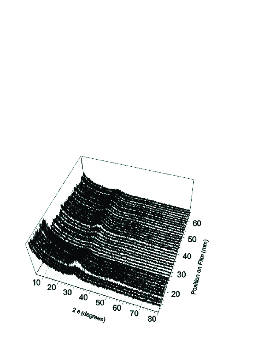
The presence of broad peaks shows the amorphous nature of the films. As such, the films must be annealed to crystallize the Bi-2212 phase.
The as-deposited film whose EDS data are shown in Figure 3 (panel B) was post annealed in a covered alumina crucible. According to Rubin [21], the deposited films can develop Bi deficiency during annealing. To compensate, they added Bi2O3 powder to enrich the atmosphere with Bi, since Bi2O3 has a lower vapor pressure than the BiO in the films [21]. Adapting the annealing regime from Tsukamoto [22] and using Rubin’s suggestion, the films were annealed as follows. The furnace was heated to 780 oC at which point the film, previously placed in a covered alumina crucible with powdered Bi2O3, was inserted. The crucible was introduced to the furnace for 0.5 hours, after which it was removed from the furnace and air quenched to room temperature. The furnace was then heated to 860 oC and the samples were again inserted into the hot furnace for 6 hours, and then removed.
X-ray diffraction patterns of the annealed film deposited on MgO are shown in Figure 5.
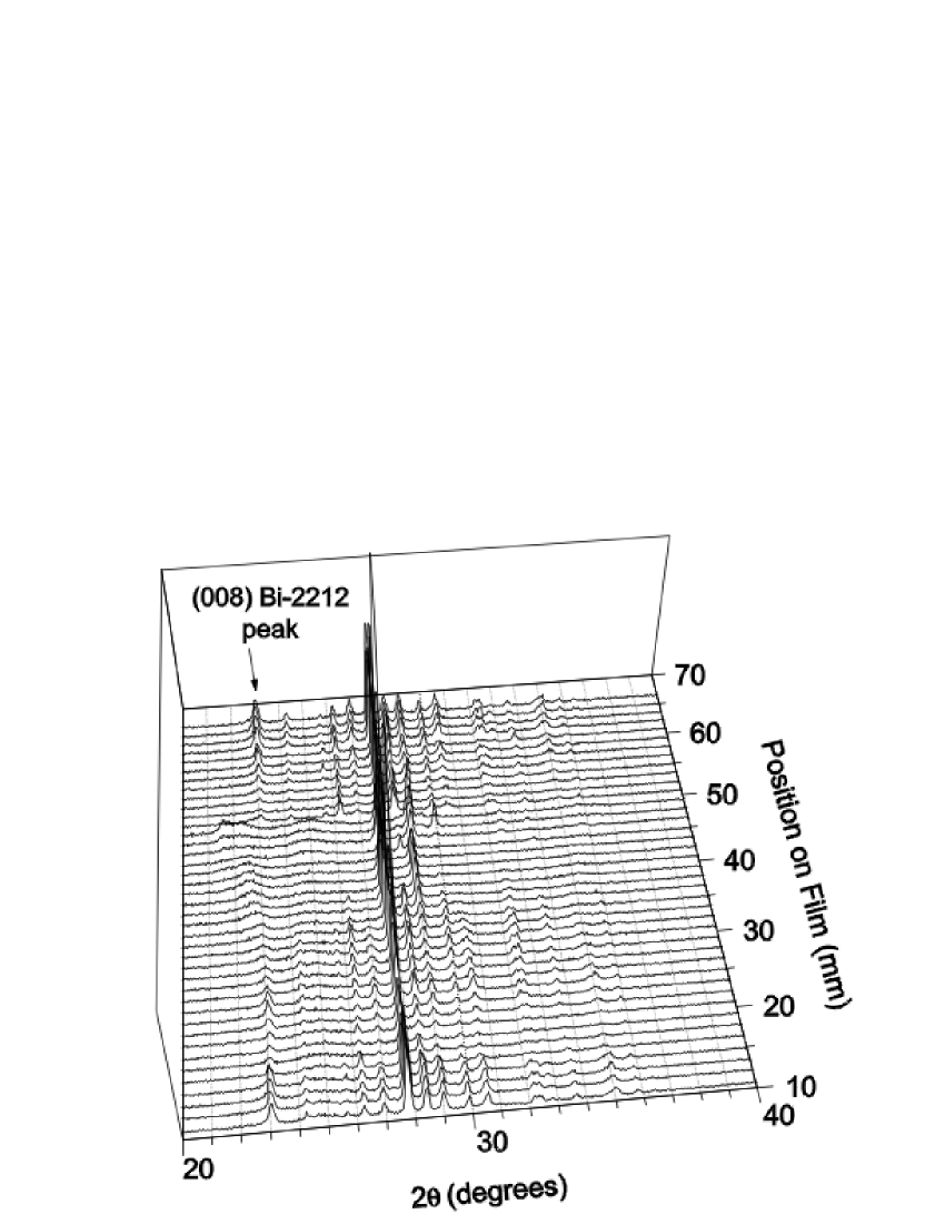
The XRD spectra reveal the presence of two major phases - the desired Bi2212 phase and a second, more dominant, Bi2SrO4 phase. Figure 6 shows the XRD spectra corresponding to a point 10.4 mm from the inner edge of the film, and the hkl indicies of the two phases.

It is possible that the Bi2SrO4 phase is induced from the presence of Bi2O3 in the anneal atmosphere [21], though there is no firm evidence of this. Figure 6 also reveals that the film exhibits epitaxial growth, since only ()=(00) X-ray peaks are observed. Thus, the films are oriented with the c-axis perpendicular to the plane of the substrate - a very desirable feature. The intensity of the (008) peak of the Bi2212 phase diminishes as the film progresses toward the center, and begins to reappear and increase in intensity past the center.
Figure 7 shows the correlation of (008) peak area with the Bi/Cu ratio as seen in Figure 3, panel B.

It is obvious that deposition of the correct Bi concentration is needed to create the desired Bi-2212 phase.
In an attempt to produce a pure Bi-2212 phase, a deposition was made with just the Bi-Ca-2212 target. This run was carried out with the same conditions as listed in Table 4. Single crystal (100) MgO substrates were placed on the edge of the film (over the last 10 mm of the sputtering track), without any physical masks. A film of approximately 1.5 m was deposited. EDS of the film is shown in Figure 8 where it is seen that the normalized data for Bi, Sr and Ca appear to have a peak in the center.
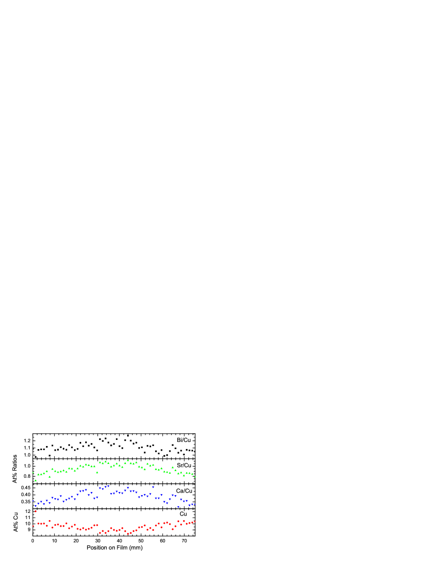
Further inspection revealed an unexpected deficiency of Cu at the center which increases the normalized atomic ratio of Bi in the center. However, near the edges the stoichiometry matches the desired ratios. This problem with Cu deficiency has not resurfaced in numerous depositions.
The film was subject to an annealing regime consisting of a quick ramp (25 oC/min) to 780 oC for one hour followed by a second identical quick ramp to 860 oC for three hours. As shown in Figure 9 the result is a partially crystalline phase.

The sharp peaks in the pattern were identified as (00) peaks of the Bi2212 phase (with two weak unidentified peaks). The (006) peak is broad demonstrating the partially amorphous nature of the annealed films. The film would have to undergo a longer anneal period to fully crystallize. However the lack of the Bi2SrO4 phase is reassuring.
Though the film composition at the edges are in the desired ratio and produce the desired phase, there is still a non-stoichiometric proportion of Bi near the centre of the film. To reduce this effect, a negative substrate bias had to be constructed to deflect oxygen anions away from the film. The film is deposited onto a rotating substrate. Thus one needs to design a rotating contact brush system. The substrates are either conductive, or have a conductive mask, consequently creating a substrate/mask bias is easily done, if an appropriate electrical contact system can be designed. Figure 10 shows a schematic of a carbon brush assembly that was manufactured on-site.
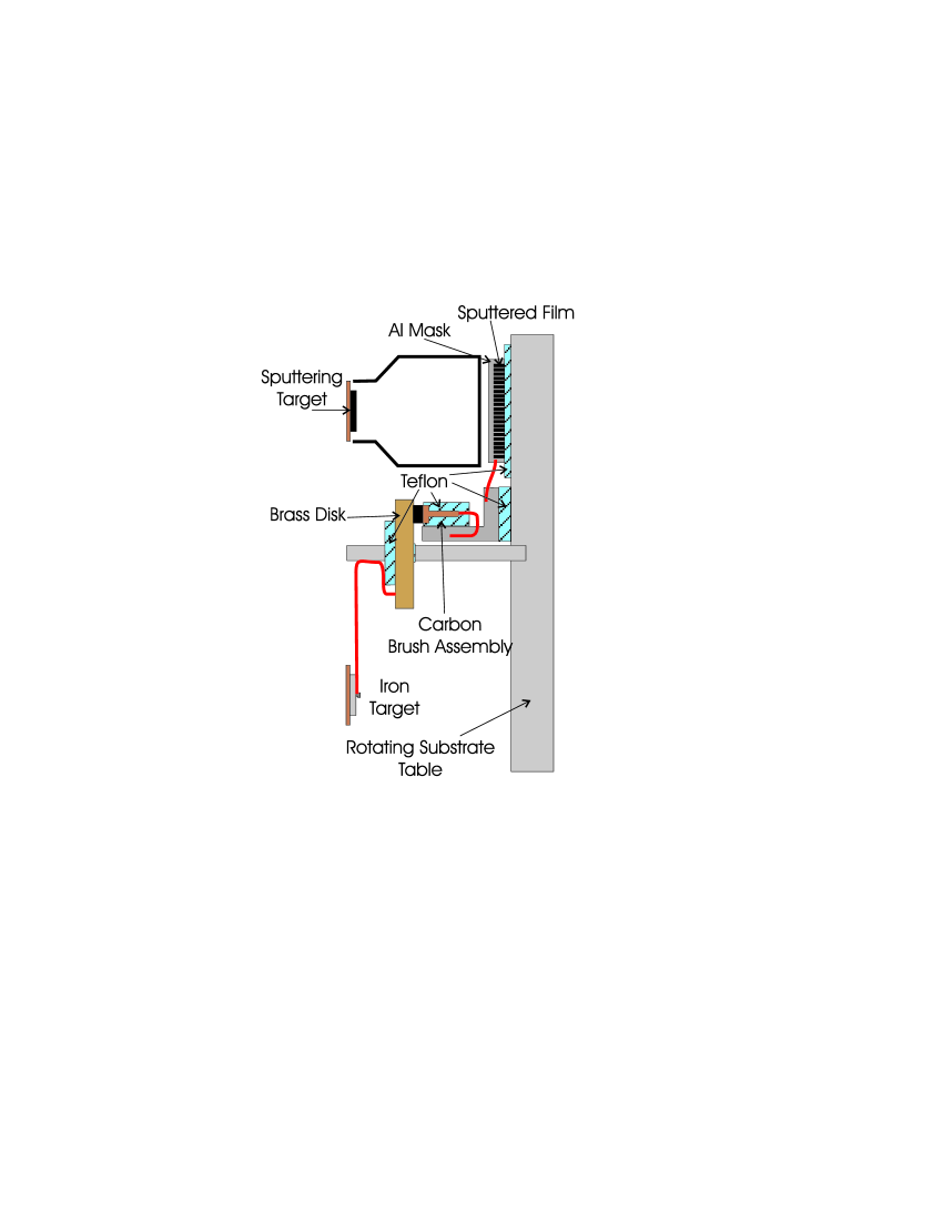
It uses an existing magnetron to supply a negative bias to the substrate.
As the substrate table rotates, the carbon brush remains in contact with the brass disk. The brass disk is fixed to a central rod which is attached to the back of the sputtering chamber. An insulated wire electrically connects the brass disk to a 7 mm thick iron target. The iron target is thick enough so that the magnetic field from the magnetron is contained in the iron and only a small bias is applied, hindering the possibility of the formation of plasma and the subsequent sputtering of the iron. During deposition, a negative bias is applied to the iron target, and through the carbon brush assembly this bias is passed to the rotating substrate table. Using insulated wires the carbon brush assembly is connected to conductive Al masks (for MgO) or Al or Si substrates. Any negative bias can be applied by the magnetron, and in this case -20 V DC was chosen. The -20 V DC bias should be enough to reduce resputtering when teamed with an increased working pressure, but not high enough to induce any sputtering of the sample from any positive ions in the chamber. The brass disk, carbon brush assembly and the substrate are electrically insulated from the chamber by Teflon insulators.
Figure 11 shows EDS data for a Bi2Sr2Ca1-xYxCu2Oy (0 0.4) deposition using the rotating substrate bias apparatus with a bias of -20 V DC, and sputtered with similar conditions to column B in Table 4.
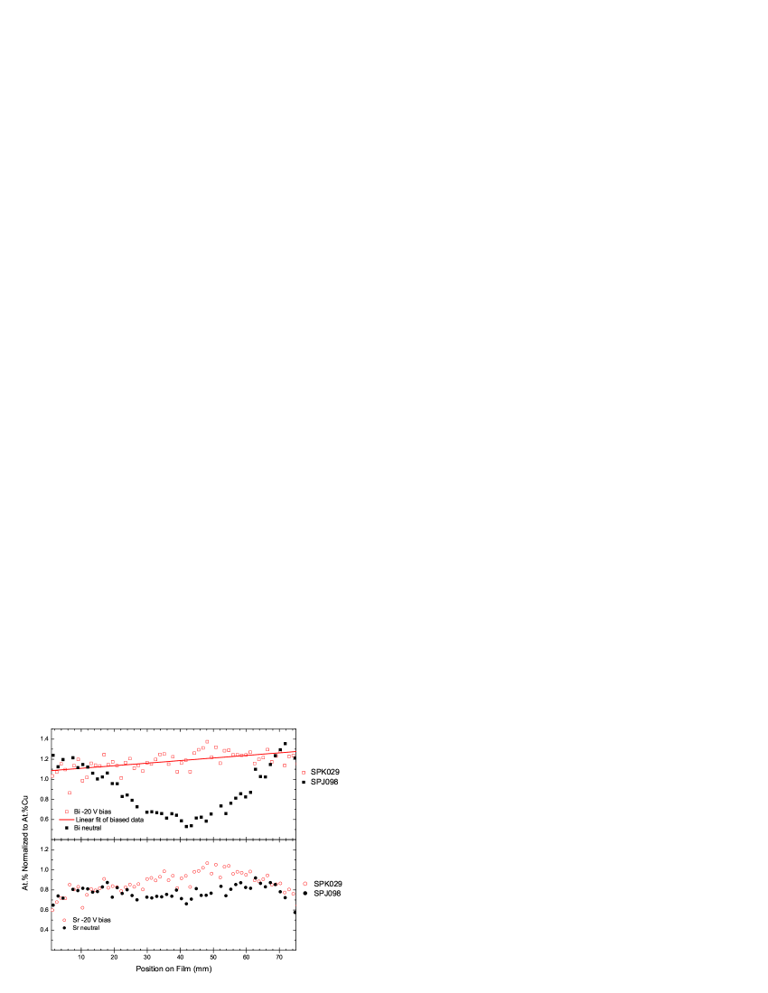
The uniformity of the normalized Bi content across the biased sample demonstrates the effectiveness of the substrate bias to eliminate the resputtering effect. The similarities between the Sr content in both samples is also reassuring, in that the composition of the Sr was not greatly affected by the sample bias.
The complete as-deposited EDS profile for co-deposition of Bi-Y-2212 and the Bi-Ca-2212 targets with a -20 V substrate bias is shown in Figure 12.
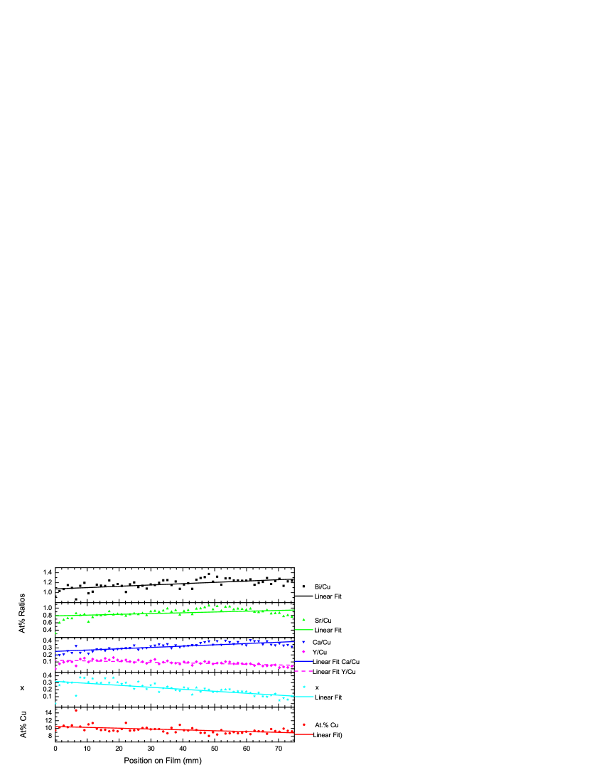
The levels of Bi, Sr and Cu are relatively constant across the film, and the ratios of Bi and Sr are consistent with the stoichiometric ratios needed to form Bi2212. For this deposition the physical mask on Bi-Ca-2212 was changed to produce a constant mass deposition across the film, while the Bi-Y-2212 target mask produced a linear gradient across the radius of the doughnut shaped sputtering track. The result is an amorphous film with the stoichiometric ratios needed to produce a set of Bi2Sr2Ca1-xYxCu2Oy films with 0.1x0.4. Post-annealing studies of the as-deposited conducted under a variety of conditions will be reported in a subsequent paper.
3 Conclusions
Composition studies demonstrate the need for correct stoichiometry across the whole film for the formation of the Bi2212 phase. Through the development of a rotating carbon brush apparatus, a -20 V DC bias can be applied to the sample substrate. The negative bias has been used successfully with an increased chamber pressure to reduce the resputtering effect across the film. Thus, with these methods, one may produce the desired stoichiometry in films prepared by the composition spread approach.
4 Acknowledgements
We would like to acknowledge valuable discussions with J. R. Dahn, A. E. George and S. Trussler. The financial support of the Natural Sciences and Engineering Research Council of Canada is gratefully acknowledged.
References
- [1] S. K. Park and J. H. Je, Physica C 245 (1995) 167.
- [2] R. H. Hammond and R. Borman, Physica C 162-164 (1989) 703.
- [3] A. C. Westerheim, L. S. Yu-Jahes and A. C. Anderson, IEEE Trans. Magn. 27 (1991) 101.
- [4] D. E. Morris, C. T. Hultgren, A. M. Markelz, J. Y. T. Wei, N. G. Asmar and J. H. Nickle, Phys. Rev. B 39 (1989) 6612.
- [5] J.M. Grace, D.B. McDonald, M.T. Reiten, J. Olson, R.T. Kampwirth and K.E. Gray, J. Vac. Sci. Technol. A 10 (1992) 1600.
- [6] J.M. Grace, D.B. McDonald, M.T. Reiten, J. Olson, R.T. Kampwirth and K.E. Gray, J. Appl. Phys. 70 (1991) 3867.
- [7] J.-H. Xu, G.-G. Zheng, A.M. Grishin, B.M. Moon, K.V. Rao and J. Moreland, Appl. Phys. Lett. 64 (1994) 1874.
- [8] S. S. Nathan, G. Mohan and S. Mohan, Thin Solid Films 347 (1999) 14.
- [9] C. Blue and P. Boolchand, Appl. Phys. Lett. 58 (1991) 2036.
- [10] P.H. Ballentine, J.P. Allen, A.M. Kadin and D.S. Mallory, J. Vac. Sci. Technol. A 9 (1991) 1118.
- [11] J.D. Klien and A. Yen, J. Vac. Sci. Technol. A 9 (1991) 1600.
- [12] J.J Cuomo, R.J. Gambino, J.M.E. Harper, J.D. Kuptsis and J.C. Webber, J. Vac. Sci. Technol. 15 (1978) 281.
- [13] K. Kennedy, T. Stefansky, G. Davy, V. F. Zackay, E. R. Parker, J. Appl. Phys. 36 (1965) 3808.
- [14] J. J. Hanak, J. Mater. Sci. 5 (1970) 964.
- [15] X. D. Xiang, X. Sun, G. Briceno, Y. Lou, K-A. Wang, H. Chang, W. Wallace-Freedman, S-W. Chen and P. Schultz, Science 268 (1995) 1738.
- [16] R. B. van Dover, L. F. Schneemeyer, R. M. Fleming, Nature 162 (1998) 392.
- [17] H. Chang, I. Takeuchi, X.-D. Xiang, Appl. Phys. Lett. 74 (1999) 1165.
- [18] X.-D. Xiang, Ann. Rev. Mater. Sci. 29 (1999) 149.
- [19] J.R. Dahn, S. Trussler, T.D. Hatchard, A. Bonakdarpour, J.N. Meuller-Neuhaus, K.C. Hewitt and M. Fleischauer, Chem. Mater. 14 (2002) 3519.
- [20] I-J. Hsu, R.-S. Liu, J.-M. Chen, R.-G. Liu, L.-Y. Jang, J.-F. Lee and K.D.M. Harris, Chem. Mater. 12 (2000) 1115.
- [21] L.M. Rubin, T.P. Orlando, and J.B. Vander Sande, Physica C 220 (1994) 284.
- [22] K. Tsukamoto, H. Shimojima, M. Ishii, N. Enomoto and C. Yamagishi, J. Am. Ceram. Soc. 76 (1993) 1031.