Three-terminal scanning tunneling spectroscopy of suspended carbon nanotubes
Abstract
We have performed low-temperature scanning tunneling spectroscopy measurements on suspended single-wall carbon nanotubes with a gate electrode allowing three-terminal spectroscopy measurements. These measurements show well-defined Coulomb diamonds as well as side peaks from phonon-assisted tunneling. The side peaks have the same gate voltage dependence as the main Coulomb peaks, directly proving that they are excitations of these states.
pacs:
73.63.Fg, 68.37.EfThe interplay between electrical and mechanical degrees of freedom is critical for understanding single-molecule devices. Changes in molecular orientation and electron-phonon coupling can have a large effect on the transport through the molecule. While there has been much theoryBoese and Schoeller (2001); Fedorets et al. (2002); Alexandrov et al. (2003); McCarthy et al. (2003); Flensberg (2003); Aji et al. (2004); Mitra et al. (2004) on this interplay, there have been relatively few experiments to datePark et al. (2000); Yu et al. (2004); Pasupathy et al. (2005). The primary difficulty in the latter has been making reproducible measurements due to variations in how the molecule couples to the electrodes. Present state-of-the-art techniques require fabricating many devices of which only a small percentage show the desired results. For fundamental studies, better control can be achieved using a scanning tunneling microscope (STM) tip as one of the contacts and performing combined scanning tunneling spectroscopy and electrical transport measurements. This allows the position and coupling of the electrode to be varied.
Single-walled carbon nanotubes (SWCNTs) are ideal single-molecules because of their well understood electrical properties and their long length that allows spatially resolved measurements. By suspending the nanotubes, the coupling to the metallic substrate is reduced, revealing Coulomb blockade behaviorLeRoy et al. (2004a). In the center of the suspended regions, we have observed additional side peaks on the Coulomb peaks which we have previously attributed to phonon-assisted tunneling LeRoy et al. (2004b). The assignment of the additional peaks as excitations of the main Coulomb peaks was due to three experimental observations. The peaks were equally spaced in voltage from the main peaks. Additional peaks appeared at higher current in analogy to photon-assisted tunneling Tien and Gordon (1963). Lastly, the peak energy scaled as the inverse of the SWCNT diameter in agreement with the energy of the radial breathing mode phonon. However, the lack of a gate electrode precluded a direct confirmation that the peaks where excitations of the main Coulomb peak.
In this paper, we show results from three-terminal scanning tunneling spectroscopy measurements on suspended SWCNTs. We have added a gate electrode into the device design in order to allow three-terminal electrical measurements. Using the gate electrode, we are able to access the full Coulomb diamond as a function of both substrate and gate voltage and to accurately determine the capacitances between the SWCNT and the tip, substrate, and gate. We are also able to determine the origin of the phonon-assisted tunneling side peaks, confirming that the peaks are indeed excitations of the main elastic Coulomb peaks. Furthermore, we report additional features in the spectra, in particular avoided crossings between sets of differential conductance peaks.
The samples consisted of individual single-wall carbon nanotubes freely suspended across trenches etched in SiO2 or Si3N4. The sample preparation has been described previously for the Si3N4 samples Kong et al. (2005). The fabrication of the SiO2 samples was similar except that the trenches were only etched 150 nm into the 250 nm thick oxide layer. This was followed by deposition of Pt at a 60 degree angle from the normal to prevent the metal from reaching the bottom of the trench. With this method, we can use the Si as a back gate because there is no metal in the trench to screen the gate. This also eliminates the possibility of short circuits between the Pt substrate and the gate electrode because the gate is still covered by 100 nm of SiO2. During scanning tunneling microscopy imaging of the Si3N4, we observed that SWCNTs could be pushed around the surface whereas they were more firmly attached on the SiO2 sample. The reason for this difference is not understood. The only difference that we observed in the electrical properties of the two sets of samples is that the gate electrode coupled better to the SWCNTs in the Si3N4 sample because of its closer proximity to the SWCNTs.
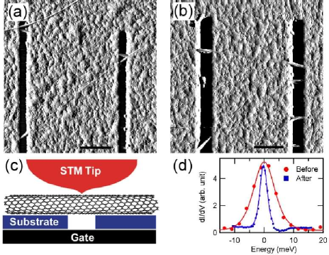
Figures 1(a) and (b) are atomic force microscope (AFM) images of SWCNTs grown across 100 and 200 nm wide trenches, respectively. Figure 1(c) is a schematic diagram showing a SWCNT crossing a trench with the STM tip, substrate and gate labelled.
All the STM measurements were made in a low-temperature ultra-high vacuum scanning tunneling microscope (STM) operating at 5 K. The commercial STM (Omicron LT-STM) has been modified to decrease the electron temperature and allow three-terminal measurements. In order to decrease the electron temperature, all the wires going to the STM were heat sunk to a large Cu rod connected to the Li-He vessel. This lowered the effective electron temperature from 25 K to about 5 K. This can be seen in Fig. 1(d) where two Coulomb blockade peaks are plotted before (red) and after (blue) the modifications to the STM. Although the electron temperature was greatly reduced the temperature measured by the Si sensor diode remained nearly constant at 4.6 K. We have also modified the sample holders to allow three electrical contacts to be made. This allows separate source, drain, and gate contact to the sample.
SWCNTs crossing trenches were located using scanning tunneling microscopy. Typical settings for STM measurements were a gap voltage of -0.5 V applied to the Pt substrate with respect to the grounded STM tip, and a feedback current of 300 pA. After finding suspended SWCNTs, spectroscopy measurements were performed on the suspended portion. The spectroscopy was performed by stabilizing the current and then turning off the feedback circuit and measuring the current as a function of the substrate voltage. The differential conductance, dI/dV was measured by adding a small ac voltage (2-4 mV rms, 887 Hz) and using lock-in detection.
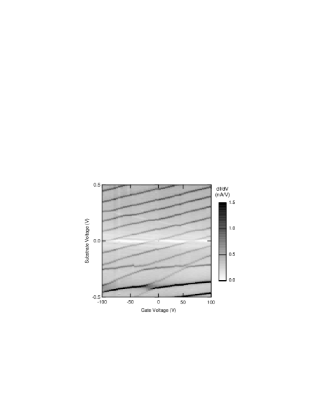
The addition of a gate electrode in the scanning tunneling microscopy setup allows the electronic behavior of the suspended nanotubes to be fully investigated. By changing the gate voltage, the number of electrons on the nanotube changes. Figure 2(a) plots the differential conductance as a function of gate and substrate voltage. Diamond-shaped regions of zero current (white area) are visible, demonstrating the Coulomb blockade effectGrabert and Devoret (1992); Kastner (1992). When the substrate voltage is zero, moving horizontally from one diamond to the next corresponds to changing the number of electrons on the SWCNT by one. The edges of the diamond correspond to the Fermi level of either the tip or the substrate lining up with a filled or empty state of the SWCNT.
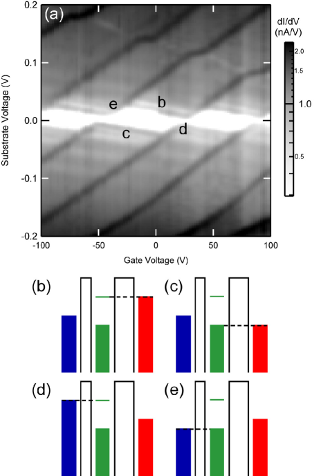
Access to the full Coulomb diamond plot allows the unambiguous identification of the origin of all the peaks in the measurements. The strong peaks running from the bottom left to the top right of Fig. 2(a) are due to the Fermi level of the substrate aligning with a state on the SWCNT. A schematic of the energy levels for these lines are shown in Fig. 2 (d) and (e). These lines are strong because of the large asymmetry in the tunnel barriers. When the Fermi energy of the substrate passes an empty state on the dot, the state is filled and the energy of the other states shift upward by the charging energy. This brings many more states into the bias window which can then tunnel out the tip lead giving a large peak in the conductance. The weaker lines running in the other direction are from the tip aligning with states in the SWCNT. Fig. 2 (b) and (c) are schematics showing the energy levels giving rise to these lines. The lines appear much weaker because the total tunnel rate through the SWCNT is controlled by the tip lead and this process only leads to one new state that electrons from the tip can tunnel into. Therefore there is only a small change in the current and the peaks are only visible at low sample voltage and current.
From the size of the Coulomb diamonds and the slope of their edges, we can determine the three capacitances in our measurement as we have done previouslyKong et al. (2005). The three capacitances are the tip to the SWCNT, Ctip, the SWCNT to the substrate, Csub, and the SWCNT to gate capacitance, Cg. The gate capacitance is found using the equation where Vg is the width of the diamond in gate voltage. This equation assumes that the level spacing of the SWCNT is small. If this is not the case, then the widths of the Coulomb diamonds would vary because of the additional energy caused by the level spacing. For this SWCNT, we see no variation in the size of the Coulomb diamonds and therefore we conclude that the level spacing is small. From the width of the diamond, we find a value of Cg of 2 zF. The height of the diamond gives the charging energy Ec. This is related to the total capacitance CΣ using the equation . From the height of the Coulomb diamond, we get CΣ 6 aF. The slope of the edge of the diamond going towards the bottom right is given by allowing us to determine the value of Csub. We find that Csub 4.6 aF. The last capacitance can be found by the slope of the other lines, , yielding Ctip 1.4 aF. As a further consistency check, the sum of the three capacitances can be compared with CΣ.
The experimental values found for the capacitances are in reasonable agreement with electrostatic simulations of our device structure. We modelled the tip as a 150 nm radius sphere and the SWCNT as a 2 nm diameter cylinder. We then calculated the capacitance between the SWCNT and the tip, substrate and gate electrode. We find that the calculated Csub is about 2 aF but depends on the length of the SWCNT quantum dot over the Pt. A simple estimate for the capacitance of the SWCNT to the substrate can be given by considering an infinite cylinder lying above a conducting plane. This has a capacitance per unit length of where d is the distance of the center of the cylinder above the plane and R is the radius Scott (1966). If we use d = 1.25 nm and R = 1.0 nm, then the capacitance is 2.5 aF for every 30 nm. From this, we conclude that our SWCNT quantum dot does not extend very far over the Pt substrate.
In previous measurements on suspended SWCNTs, we have observed additional peaks which were attributed to phonon-assisted tunneling. LeRoy et al. (2004b) The assignment of the peaks as phonon side peaks was based mainly on three factors: they were equally spaced from the main Coulomb peaks, additional peaks appeared at high current, and their energy varied as a function of SWCNT diameter. Despite this evidence, another possibility was that the side peaks were not excitations of the main Coulomb peak but rather due to tunneling at the other junction. In this scenario, the appearance of new peaks at high currents would be the result of a decreasing . While this scenario was found to be unlikely based on quantitative analysis of peak spacing, a gate electrode provides more definitive evidence; if the peaks were due to the tip lead, the sign of their slope with gate voltage would be the opposite of the main Coulomb peaks.
Figure 3 shows the differential conductance as a function of sample and gate voltage at two different setpoint currents. Fig. 3(a) is taken with the feedback current stabilized at 300 pA at -0.5 V while Fig. 3(b) has a current of 500 pA at -0.5 V. Once again, there are peaks running from the bottom left to the top right due to the addition of electrons to the SWCNT. These peaks are due to the Fermi level in the substrate lining up with a state on the SWCNT. The peaks running in the other direction, due to the Fermi level of the tip lining up with a state on the SWCNT, are too faint to be resolved in this measurement due to the large tip resistance. However, there are side peaks running parallel to the main peaks due to phonon-assisted tunneling LeRoy et al. (2004b). In this case, the side peaks are most prominent for negative sample voltages. Figs. 3(c) and (d) are zoom-ins on the negative voltage region of (a) and (b) respectively. The fact that the side peaks run parallel to the main peak confirms that they are an excitation of this state, ruling out the possibility that they are the faint peaks due to the Fermi level of the tip lining up with a state on the SWCNT. Therefore, we can assign these phonon peaks to electrons tunneling between the SWCNT and the substrate lead. Knowing the origin of the phonon side peaks allows their energy to be calculated from their spacing from the Coulomb peak. Since they are due to the substrate lead, we must scale their measured voltage from the Coulomb peak by the fraction of the voltage that drops at this junction. This gives a scaling factor of . The incorporation of the gate electrode and measurement of the Coulomb diamond allows a more accurate determination of the phonon energy because the capacitances can be better measured from the slopes of the diamonds.
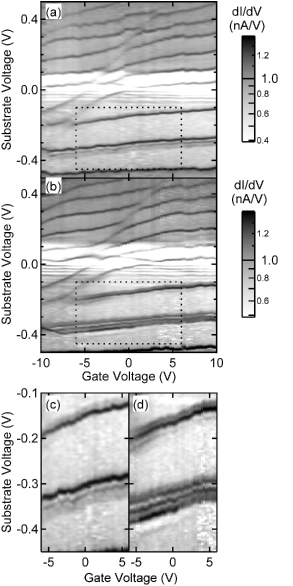
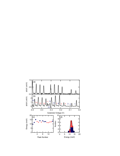
The strength of the phonon side peaks can be controlled by the current through the SWCNT LeRoy et al. (2004b). Figs. 3(c) and (d) demonstrate the effect of increasing the current. At higher current, 3(d), the side peaks are more pronounced and additional ones are present. Figures 4(a) and (b) plot the differential conductance as a function of energy at two different setpoint currents. At low setpoint current, 100 pA at -0.6 V (Fig. 4(a)), groups of four Coulomb peaks are visible but there are no phonon side peaks. The groupings are caused by the two spin-degenerate bands of the SWCNT. This allows level spacing in this SWCNT to be measured, which we find to be about 30 meV. At higher setpoint current, 300 pA (Fig. 4(b)), additional peaks become visible. The side peaks are equally spaced in energy from their associated Coulomb peaks and can occur on either side of their associated Coulomb peak. This implies that they are due to both emission and absorption of phonons. The fact that they are equally spaced can be seen in Figure 4(c), which plots the peak energy for a series of 15 side peaks. The blue squares plot the energy for peaks associated with emission of a phonon, while the red circles are for absorption. These energies have been converted from the substrate voltage using the scaling factor . This takes into account that only a fraction of the voltage drops at the substrate-SWCNT junction. Because this device did not have a gate electrode, the values of and were determined from the spacing of the Coulomb peaks and the values of the differential conductance Hanna and Tinkham (1991). Figure 4(d) is a histogram of the energies showing that both the absorption and emission side peaks have similar energies. For this 2.5 nm tube the phonon energy is measured to be 11.8 1.4 meV. The uncertainty corresponds to the standard deviation of the Gaussian fit in Fig. 4(d). This agrees well with the theoretical energy of the radial breathing mode, which is 11.5 meV. Dresselhaus and Eklund (2000)
The SWCNT phonon density of states includes many more modes which are not observed in the measurements. The low-energy string modes can not be resolved because their energy is much lower than kT. For a 100 nm long SWCNT, their energy is 0.014 meV which is 30 times smaller than kT.Sapmaz et al. (2003) Recent calculations show that the electron-phonon matrix element is largest near =0 for the radial-breathing and optical phonons Perebeinos et al. (2005). However, experimentally the high-energy optical phonons (200 meV) are not observed. The theoretical calculations do not consider the local tunneling nature of the STM experiment, which may influence the relative strengths of the phonon peaks. In particular, the speed that the electron spreads out around the SWCNT compared to the frequency of the phonon makes circumferentially symmetric modes more likely to be excited. The high energy, long wavelength and high symmetry of the radial-breathing mode make it the easiest phonon to excite.
In most of our measurements of differential conductance as a function of gate and sample voltage, we observe some Coulomb peaks that do not run parallel to the others. Figure 5 shows an example of this in the negative substrate-voltage portion of the plot. There are two peaks that are only weakly dependent on the gate voltage, being nearly horizontally. This implies that these peaks have a different coupling to the gate from the main series of peaks. There is also a faint dip in the positive substrate voltage region whose origin is unknown. Because not all the peaks are parallel, there are locations where they cross. Three such crossings can be seen in Fig. 5. When this occurs, the peaks show an avoided crossing behavior rather than a simple intersection. The fact that the peaks do not cross implies that there is a coupling between these two states. The origin of these extra peaks is unknown, but this type of feature may arise from localized states caused by a defect in the SWCNT, or a second quantum dot in parallel. Based on topography and spectroscopy, we believe that all of the nanotubes that we have measured have been isolated singe-walled tubes. Therefore, it is unlikely that the avoided crossings arise from interaction between two SWCNTs in a rope. Future measurements probing the spatial extent of these extra peaks may allow their origin to be identified.
In summary, we have shown scanning tunneling spectroscopy measurements on the free-standing portion of suspended SWCNTs with an integrated gate electrode. The differential conductance shows sharp spikes corresponding to the addition of electrons to the SWCNT along with side peaks due to phonon-assisted tunneling. The entire Coulomb diamond plot is accessed using the gate electrode. Furthermore, the gate electrode is used to confirm that the side peaks arising at high currents correspond to excitations of the main Coulomb peaks. This supports the interpretation that they represent phonon-assisted electron transport.
Our measurements leave three main unresolved issues that require more theoretical and experimental work; 1) many of the SWCNTs show Coulomb blockade behavior as prepared (i.e. without being cut by the STM tip) implying that there is a tunneling barrier between the SWCNT and the Pt substrate. More work needs to be done to determine if this barrier is formed by defects near the edge of the trench, band bending, or some other mechanism. 2) Phonon-assisted side peaks are only observed near the center of the suspended SWCNTsLeRoy et al. (2004b). Why are the phonons preferentially excited in this region when the electronic wavefunction is extended over the entire suspended region of the SWCNT? 3) Previously, we have studied the strength of the phonon-assisted side peaks as a function of current through the SWCNTLeRoy et al. (2004b). We found that the amplitude of the side peaks scaled as a Bessel function in analogy to photon-assisted tunnelingTien and Gordon (1963). Experimentally we found the argument of the Bessel function scaled linearly with the current. However, the electron-phonon term in the Hamiltonian scales with the square root of the number of phonons and hence current. The origin of this discrepancy must still be addressed with more experimental measurements and theoretical work.
Acknowledgements.
The authors would like to thank Ya. Blanter and Y. Nazarov for helpful discussions and I. Heller for help with the sample growth. This research was supported by Stichting voor Fundamental Onderzoek der Materie (FOM) and the Netherlands Organization for Scientific Research (NWO).References
- Boese and Schoeller (2001) D. Boese and H. Schoeller, Europhysics Letters 54, 668 (2001).
- Fedorets et al. (2002) D. Fedorets, L. Y. Gorelik, R. I. Shekhter, and M. Jonson, Europhysics Letters 58, 99 (2002).
- Alexandrov et al. (2003) A. S. Alexandrov, A. M. Bratkovsky, and R. S. Williams, Phys. Rev. B 67, 075301 (2003).
- McCarthy et al. (2003) K. D. McCarthy, N. Prokof ev, and M. T. Tuominen, Phys. Rev. B 67, 245415 (2003).
- Flensberg (2003) K. Flensberg, Phys. Rev. B 68, 205323 (2003).
- Aji et al. (2004) V. Aji, J. E. Moore, and C. M. Varma, International Journal of Nanoscience 3, 255 (2004).
- Mitra et al. (2004) A. Mitra, I. Aleiner, and A. J. Millis, Phys. Rev. B 69, 245302 (2004).
- Park et al. (2000) H. Park, J. Park, A. K. L. Lim, E. H. Anderson, A. P. Alivisatos, and P. L. McEuen, Nature 407, 57 (2000).
- Yu et al. (2004) L. H. Yu, Z. K. Keane, J.W. Ciszek, L. Cheng, M. P. Stewart, J. M. Tour, and D. Natelson, Phys. Rev. Lett. 93, 266802 (2004).
- Pasupathy et al. (2005) A. N. Pasupathy, J. Park, C. Chang, A. V. Soldatov, S. Lebedkin, R. C. Bialczak, J. E. Grose, L. A. K. Donev, J. P. Sethna, D. C. Ralph, et al., Nano Letters 5, 203 (2005).
- LeRoy et al. (2004a) B. J. LeRoy, S. G. Lemay, J. Kong, and C. Dekker, Appl. Phys. Lett. 84, 4280 (2004a).
- LeRoy et al. (2004b) B. J. LeRoy, S. G. Lemay, J. Kong, and C. Dekker, Nature 432, 371 (2004b).
- Tien and Gordon (1963) P. K. Tien and J. P. Gordon, Phys. Rev. 129, 647 (1963).
- Kong et al. (2005) J. Kong, B. J. LeRoy, S. G. Lemay, and C. Dekker, Appl. Phys. Lett. 86, 112106 (2005).
- Grabert and Devoret (1992) H. Grabert and M. H. Devoret, Single Charge Tunneling (Plenum, New York, 1992).
- Kastner (1992) M. Kastner, Rev. Mod. Phys. 64, 849 (1992).
- Scott (1966) W. T. Scott, The Physics of Electricity and Magnetism” (John Wiley and Sons, Inc., 1966), 2nd ed.
- Hanna and Tinkham (1991) A. E. Hanna and M. Tinkham, Phys. Rev. B 44, R5919 (1991).
- Dresselhaus and Eklund (2000) M. S. Dresselhaus and P. C. Eklund, Advances in Physics 49, 705 (2000).
- Sapmaz et al. (2003) S. Sapmaz, Y. M. Blanter, L. Gurevich, and H. S. J. van der Zant, Phys. Rev. B 67, 235414 (2003).
- Perebeinos et al. (2005) V. Perebeinos, J. Tersoff, and P. Avouris, Phys. Rev. Lett. 94, 086802 (2005).