Individual charge traps in silicon nanowires: Measurements of location, spin and occupation number by Coulomb blockade spectroscopy
Abstract
We study anomalies in the Coulomb blockade spectrum of a quantum dot formed in a silicon nanowire. These anomalies are attributed to electrostatic interaction with charge traps in the device. A simple model reproduces these anomalies accurately and we show how the capacitance matrices of the traps can be obtained from the shape of the anomalies. From these capacitance matrices we deduce that the traps are located near or inside the wire. Based on the occurrence of the anomalies in wires with different doping levels we infer that most of the traps are arsenic dopant states. In some cases the anomalies are accompanied by a random telegraph signal which allows time resolved monitoring of the occupation of the trap. The spin of the trap states is determined via the Zeeman shift.
pacs:
73.23.Hk, 71.70.Ej, 72.20.MyI Introduction
Single electron charges or spins are very appealing as logic bits, either as ultimate classical bits or quantum bits if coherence is usedElzerman et al. (2004); Gorman et al. (2005). To read such bits, either quantum point contacts or single electron transistors (SETs) are used. SETs have indeed been used as very sensitive electrometers for the (time-averaged) charge on a second quantum dot for over a decade now.Lafarge et al. (1991); Molenkamp et al. (1995). More recently the radio-frequency SET techniqueSchoelkopf et al. (1998) was used to monitor the charge on the second dot or to measure a current by electron counting. Lu et al. (2003); Fujisawa et al. (2004); Gustavsson et al. (2006); Bylander et al. (2005). This allows to measure lower currents than standard measurements and gives access to the full counting statistics of the current Utsumi et al. (2006).
Such experiments are difficult because any device that involves detection of few or single electron charges is subject to the dynamics of surrounding charge traps. Jung et al. (2004) This is particularly critical for metallic SETs. Zimmerman et al. (1997) For SETs based on the very mature silicon CMOS technology the control of this offset charges seems to be better. Jehl et al. (2002)
These charge traps are quantum dots whose presence or properties are not controlled. Typically they consist of defects on atomic scale. Their sizes are therefore much smaller than what is possible for lithographic quantum dots. If their positions, although being random, can be limited to some zone, the charge traps are not necessarily a nuisance but can useful. An example are flash memories where the trend is to replace the lithographic floating gate by grown silicon nanocrystals inside the gate oxide. They are grown in a layer and have all the same distance from channel and gate electrode. Their dynamics are therefore very similar. Yano et al. (1994); Molas et al. (2004) Another example are dopants in semiconductors. Efforts are made to control their individual position in a silicon crystal. Schofield et al. (2003) Indeed, besides the location, their properties are very uniform and solid state quantum bits based on dopants in a silicon crystal –individually addressed by gates and contacts– were proposed as solid state quantum bits Loss and DiVincenzo (1998); Kane (1998); Hollenberg et al. (2004). Silicon is interesting as host material because the spin relaxation time can be very longTyryshkin et al. (2003) compared to GaAs. The detection of spins of individual traps in a silicon field effect transistor has been recently reported using random telegraph noise Xiao et al. (2003, 2004). However, in this experiment the traps seem to be in the oxide rather than in the silicon.
In this work, we use nanowire-based silicon transistors operated as SETs at low temperature to detect the location, spin and occupation number of individual charge traps, which we attribute to As dopant states. They are capacitively coupled to the SET. Therefore they induce anomalies in the otherwise very regular periodic oscillations of the drain-source conductance versus gate voltage . We compare the data with simulations obtained after solving the master equation for the network formed by the main dot and the charge trap.
Not only the static time-averaged current is analyzed but also the switching noise which appears near the degeneracy point in gate voltage where the trap occupation number fluctuates.
Finally, a magnetic field was applied in order to probe the spin polarization of the traps via their Zeeman shifts. As expected from simple considerations Shklovskii and Efros (1984), we observed a majority of singly occupied traps.
II Samples and Setup
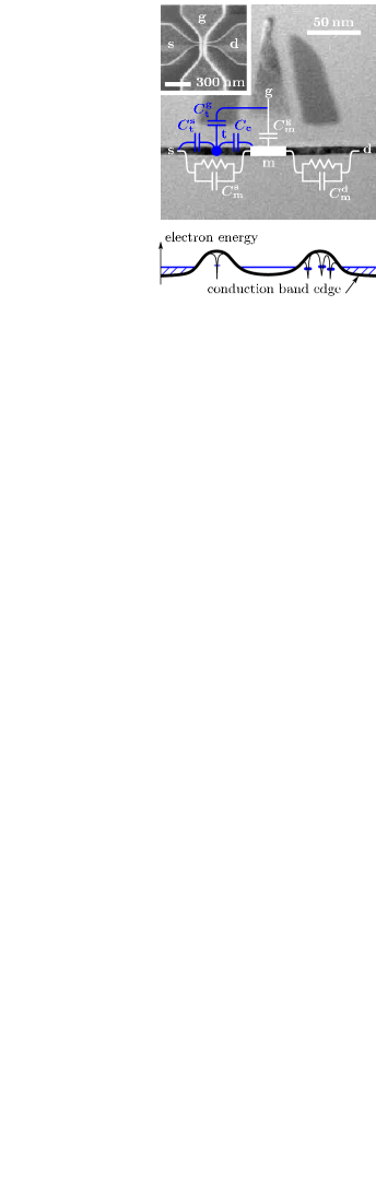
Samples are produced on silicon on insulator (SOI) wafers with buried oxide and a boron substrate doping of . The SOI film is locally thinned down to approximately and a wide and long nanowire is etched from it. A long polysilicon control gate is deposited in the middle of the wire (see Fig. 1). There are two layouts. Type A: The wires are uniformly doped with As, above . The gate oxide is . Type B: The wires are first uniformly doped at a lower level (As, ), then, after deposition of the gate electrode and -wide spacers on both sides of it, a second implantation process increases the doping to approximately in the uncovered regions while the doping level stays low near the gate. In this layout the gate oxide is 10 or thick, with a 2 or thermal oxide and 8 or deposited oxide. Most measurements are made on type B samples, and we use type A samples mainly for comparison.
The measurements were performed in a dilution refrigerator with an electronic base temperature of approximately . We used a standard 2-wire low frequency lock-in technique with low enough voltage excitation to stay in the linear regime and a room temperature current amplifier (gain ). For time resolved measurements a DC bias voltage was applied and current measured with a current amplifier (bandwidth ) followed by a AD conversion. For spin sensitive measurements a superconducting magnet was used to apply an in-plane magnetic field up to .
III Data
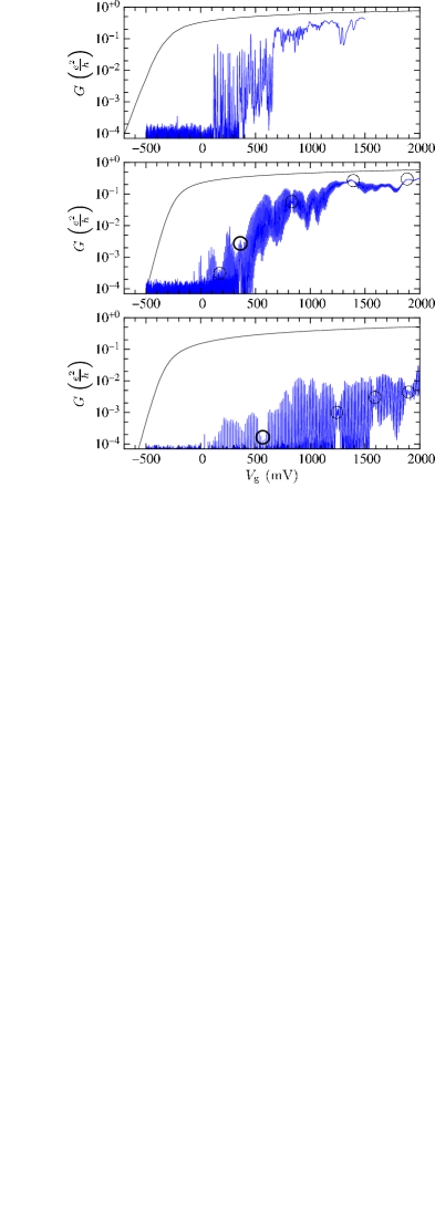
Figure 2 shows typical plots. At room temperature our samples behave as classical (albeit not optimized) -channel MOSFETs. Below approximately they turn into single electron transistors with regularly spaced Coulomb blockade resonances. The period of these oscillations ( is the absolute value of the electron charge) is determined by the gate capacitance , which in turn can be estimated from the gate/wire overlap and the gate oxide thickness. For the sample with (A), (B), (B) gate oxide the peak spacing is respectively , , . This corresponds to a gate capacitance of , , . For the type A samples the gate capacitance is in good agreement with the simple planar capacitance estimation. For the type B samples where the gate oxide thickness is of the same order as the dimensions of the wire, the 3-dimensional geometry has to be taken into account. The gate capacitance of the type B samples is increased with respect to the type A samples because the flanks of the wire play a more important role. A 3-dimensional numerical solution obtains a good agreement with the measured capacitances.
The peak spacing statistics has already been measured and compared to theory. Boehm et al. (2005) Here we focus on anomalous regions where the conductance contrast is markedly reduced and a phase shift of the Coulomb blockade oscillations occurs. This results in tails in the Gaussian peak-spacing distribution. Such perturbations to the periodic pattern are marked with circles in Fig. 2. In the type B samples with low doping, these perturbations occur only rarely (we observe typically 3 to 5 per sample). In the unperturbed regions, the height of the Coulomb blockade peaks shows long-range correlations. In the type A samples with high doping level the perturbations are more frequent and let the whole spectrum look irregular. (see top panel of Fig. 2) This suggests that the perturbations are related to the doping.
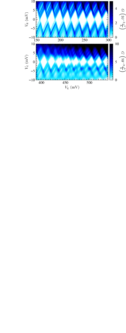
In the measured stability diagram, i.e. the 2D plot of conductance versus gate and bias voltages, the perturbations are even more visible (see Fig. 3). In the perturbed regions additional teeth appear in the Coulomb diamonds.
We develop a simple model based on a trap state located in the vicinity of the quantum dot, and compare the simulation with the experimental data.
IV Model
The quantum dot formed by the gate electrode in the middle of the wire is separated from the source and drain reservoirs by a piece of silicon wire containing only a few tens (type B) or hundreds (type A) of dopants. In the type A samples these access regions extend from the border of the gate electrode to the regions where the wire widens (see Fig. 1) and its resistance becomes negligible. In the type B samples only the zones below the spacers contribute significantly to the access resistance and the highly doped parts of the wire can be considered as part of the reservoirs.
Electrons pass through these access regions by transport via the dopant states.111Direct tunneling through a thick barrier leads to access resistances much higher than observed, even for barrier heights of a few . As the dopants are distributed randomly and the coupling between them depends exponentially on their distance, this coupling is distributed over a wide range. Transport therefore takes place mainly through a percolation path formed by well connected dopantsShklovskii and Efros (1984) while other dopant states are only weakly connected and their occupation is a good quantum number (see Fig. 1). We attribute the anomalies in the Coulomb blockade spectrum to the electrostatic interaction of the quantum dot with such a charge trap formed by an isolated dopant site.
We model this with the lumped network shown in Fig. 1. Similar models have been considered in Refs. Grupp et al., 2001 and Berkovits et al., 2005. A small trap (t) is capacitively coupled to source (s), gate (g) and to the main dot (m). We note and () After some calculation, the electrostatic energy of the two dot system can be expressed as a function of the charges on the main dot and and in the trap.
| (1) |
where is the capacitive coupling between dot and trap, , and . For a small trap () these renormalizations are weak: and . The problem is symmetric under exchange of main dot and trap even though the expression in Eq. 1 is not. is plotted in the top panel of Fig. 4.
We focus on the structure of the Coulomb blockade conductance fixed by Eq. (1) and not on the exact value on the conductance plateaus. Therefore we choose as simple as possible the following parameters which are necessary for the simulation but do not affect the structure of the conductance diagram.
We suppose all transmission coefficients to be constant, the ones connecting the main dot to source and drain being 1000 times higher than the ones connecting the trap to the main dot and source or drain. Electrons can therefore be added or removed from the trap, but their contribution to the total current through the device is negligible. This contrasts with models of stochastic Coulomb blockade Ruzin et al. (1992) or in-series quantum dots Waugh et al. (1995); Rokhinson et al. (2002) where the current has to pass through both dots.
In terms of kinetic energy, we describe the main dot as metallic (negligible single-particle level spacing , i.e. ) and we consider only one non-degenerate energy level for the trap. In source and drain we suppose a uniform density of states. We assume fast relaxation of kinetic energy inside the dot and the reservoirs, i.e. thermal distributions in the electrodes and the main dot, even for nonzero bias voltage. With these assumptions, the transition rates of an electron in the main dot to the source or drain reservoirs or from the reservoirs to the dot are proportional to the auto-convolution of the Fermi function. The transition rates from or towards the trap are directly proportional to the Fermi function. Grabert and Devoret (1992)
The statistical probability for each state of the system can now be calculated by solving numerically the master equation and gives access to the mean current through the system.
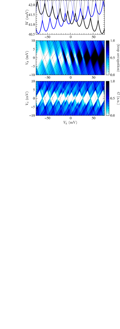
Results of such a numerical study are presented in Fig. 4. The middle panel shows the mean occupation of the trap. On a large scale, the trap becomes occupied with increasing gate voltage. In the central region of the figure however, whenever an electron is added onto the main dot, the electron in the trap is repelled and only later it is re-attracted by the gate electrode. Inversely, the trap charge repels the charges on the main dot and the Coulomb blockade structure of the main dot is shifted to higher gate voltage when the trap is occupied (see lower panel). The two Coulomb blockade structures for unoccupied and occupied trap are respectively indicated by dotted and dashed lines in the middle and lower panel of Fig. 4.
This explanation is illustrated in terms of energy in the top panel of Fig. 4, which shows the energies for the different charge configurations. The crossings of the blue (black) parabolas give the positions of the Coulomb blockade peaks for empty (occupied) trap. The shift between the crossings of the black parabolas with respect to the crossings of the blue parabolas and the shift of the dashed lines with respect to the dotted lines are due to the term in . Knowing that one Coulomb blockade oscillation corresponds to a change of in , the shift due to is
| (2) |
where is the Coulomb blockade peak spacing of the main dot.
We will now determine the width of the anomaly in the Coulomb blockade spectrum at low bias voltage. It is given by the gate voltage range where the occupation of the trap oscillates at zero bias. In the top panel of Fig. 4 this is the zone between the first and the last crossing of the thick black line and the thick blue line. First we calculate , the difference of the ground state energies for empty and occupied trap arising from the term in Eq. 1. Then we calculate the change in gate voltage necessary for to exceed this difference.
reaches its extreme values when for one state of the trap main dot is at a degeneracy point (the kinks in the thick lines), where . For the other state of the trap the main dot is a fraction of a Coulomb blockade period away from the degeneracy point and . The extrema of are therefore .
The gate voltage dependence of term is given by . Note that is the long-range gate voltage lever arm of the trap over several Coulomb blockade oscillations, where the charge of the main dot has to be considered as relaxed with the source and drain Fermi levels. has to pass form to in order to toggle the trap definitively. The width of the anomaly is therefore given by or
| (3) |
is the number of anomalous periods and with the gate voltage lever arm of the main dot.
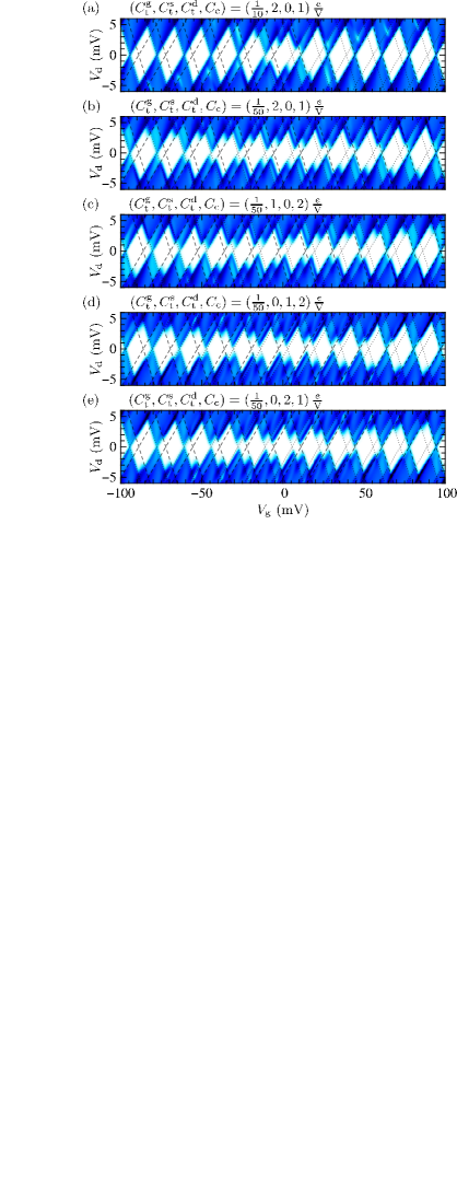
We have identified and as parameters that determine the structure of the trap signature. Both do not depend on the absolute value of the trap’s capacitances. Indeed, if one allows only 0 or 1 electron in the trap, the absolute value of the trap capacitances enters the problem only indirectly by modifying slightly the capacitance matrix of the main dot and cannot be obtained in the limit of a small trap. Our model contains therefore only 2 effective parameters for the trap instead of 3 (, , ). All 3 parameters of the trap are only significant if the trap can accommodate 2 or more electrons. In this case the spacing between the anomalies gives access to the absolute values of the trap’s capacitances
Figure 5 illustrates the relation between the trap’s capacitance matrix and its signature. If teeth of constant width for all anomalous resonances are visible at the positive slope of the Coulomb blockade diamonds, the trap is on the source side of the dot. If they are visible at the negative slope, the trap is on the drain side. The width of the teeth depends on , the width of the anomalous region essentially on (for close to where the anomalies are well visible).
V Position and nature of the traps
As an illustration, from the lower panel of Fig. 3 we infer and . These are the actual parameters that have been chosen for the simulation in Fig. 4 and the lower panels of Fig. 3 and Fig. 4 are indeed very similar. As for all impurities we observed, is small. This is what we expect for a trap inside the silicon wire. The coupling to the gate electrode is much weaker than the coupling to the main dot or the source electrode because the dielectric constant of the oxide barrier () is much smaller than that of bare silicon (), which in addition is enhanced near the insulator–metal transition. Imry et al. (1982)
Positions of the trap outside the wire can be ruled out. Traps located deep inside the oxide can be excluded because their transmissions would be too weak to observe statistical mixing of occupied and unoccupied trap states during our acquisition time below . Similar devices including intentional silicon nanocrystals at the interface between thermal oxide and deposited oxide have been studied in views of memory applications. Molas et al. (2004, 2005) The measured lifetime of charges in the nanocrystals exceeds by orders of magnitude already at room temperature and at low temperature gate voltages of about have to be applied in order to toggle the charge in the nanocrystals. The traps must therefore be inside the Si wire or at its interface with the oxide. But the interface traps are unlikely. We estimate their density to be smaller than , corresponding to a few units per sample. As they are distributed throughout the entire band gap it is very unlikely to observe several of them in the small energy window that we scan in our measurement. The most likely traps are therefore defects in the silicon wire or As donor states. Given the volume of the access regions under the spacers and the doping level , there are around 70 donor states under the spacers in devices of type B. We estimate the width of the impurity band to be . Shklovskii and Efros (1984) One should therefore expect around 15 dopants in the energy window. Typically we record 3 to 5 anomalies. Indeed we do not expect to observe anomalies for all dopants because the charge on well connected dopant sites is not quantified and, according to our model, dopants very close to the dot () or to the reservoir () produce very small anomalies.
In the type A samples the doping level in the access regions is more than 10 times higher than in the type B samples. The whole Coulomb blockade spectrum should therefore be anomalous. Indeed, the spectrum is much less regular (see Fig. 2) than for the type B samples, especially for low gate voltage, but we cannot distinguish signatures as clear as in the type B samples. This is consistent because in the type A samples the mean distance between impurities is less than and they are too well connected for the charge on them to be well quantified. In other words, the wire is very close to the insulator–metal transition. Our doping level is in fact already higher than the bulk critical As concentration . Castner et al. (1975); Shafarman et al. (1989)
We have deduced that the observed traps lie inside the wire. The position of the trap along the wire can also be determined. Traps on the source side and the drain side of the dot can be distinguished (see Fig. 5, the teeth of constant width appear on the positive slope of the diamonds in case of a trap on the source side of the dot and on the negative slope in case of a trap on the drain side) and the parameter gives the ratio between the capacitances towards the main dot and the source (or drain) electrode. As the dielectric constant of the wire is much higher than the surrounding silicon oxide, this ratio can be translated linearly to a position in direction of the wire. In the example of Fig. 3 with we would expect the impurity to be located on the way from the dot (border of the gate electrode) to the source reservoir (source side border of the spacer).
VI Time-resolved occupation number
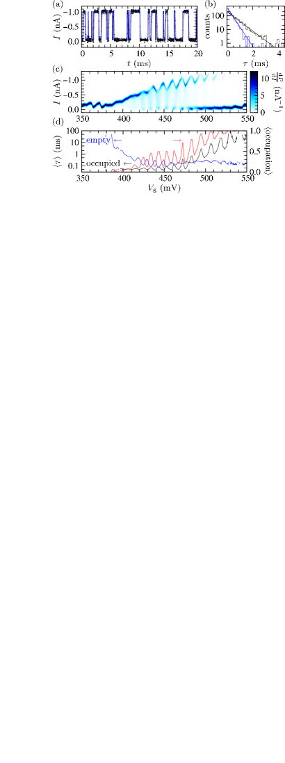
In the preceding sections we assumed charge traps with changing mean occupation number to explain anomalies in the mean conductance through a Coulomb blockaded quantum dot. Yet the measurements of the mean current have not allowed us to measure the occupation number of the trap directly. But the currents through the main dot differ for empty and occupied trap because the position of the Coulomb blockade resonances is shifted, and at the anomalies where the occupation number of the trap is different from 0 and 1, the fluctuations of the occupation number should create a random telegraph signal (RTS)Kirton and Uren (1989); Xiao et al. (2003, 2004); Buehler et al. (2004) in the current through the main dot.
Indeed, we frequently observe strongly increased current noise near the anomalies, especially at low gate voltage. However, at most anomalies at higher gate voltage we do not observe a clear increase of the noise level. This indicates that changes in the trap state occur at frequencies far beyond , the bandwidth of our measurement. Indeed, for charge traps formed by dopants we would expect the transmission rates of the trap to be of the same order as for the main dot, where the transmission occurs also through dopant states. The excess noise of the trap should therefore be comparable to the shot noise of the quantum dot, which does not emerge from the noise floor of the current amplifier. But much smaller transmissions should also be possible as the dopants are distributed randomly and the transmission rate depends exponentially on the distance between them. In some cases we observe clear RTS with time constants larger than . An example is given in Fig. 6(a). The distribution of the times spent in the two states follows the exponential distribution expected for a RTS (see Fig. 6(b)).
The color plot of the current distribution in Fig. 6(c) shows the evolution of the the two current levels (dark lines with high probability) with gate voltage. Above the two levels are very different. This difference is most likely due to electrostatic interaction of the trap and the current path through the barrier: depending on the state of the trap, the dopants through which the main part of the current flows are well or poorly aligned in energy. The fact that the current levels never cross simplifies greatly the assignment of the high and low current levels to the states of the trap. The high current trace being most likely at low gate voltage and the low current trace being most likely at high gate voltage allows to attribute the high current to empty trap and the low current to occupied trap.
The time constants of the empty and occupied state are plotted in Fig. 6(d). Consistently with panel (c), the time constant for the empty trap decreases with gate voltage while the time constant for the occupied trap increases. Superimposed with this slow change there are oscillations with a period of , the peak spacing of the main dot. This oscillation is even more prominent in the mean occupation number given by . As explained in section IV for the case of low bias, this oscillation is due to the discrete charge on the main dot which cycles the trap several times between empty and occupied state. It is not observed in RTS in larger devices without Coulomb blockadeKirton and Uren (1989). At high bias () only an oscillation of the occupation probability remains of this cycling. This can be seen in Fig. 7(b) and (d) where the occupation probability for different bias voltages is compared with simulation. As in Fig. 4, the oscillations in Fig. 7(b) and (d) are aligned parallel to the negative slopes of the Coulomb blockade diamonds indicating that the trap is on the source side of the dot.
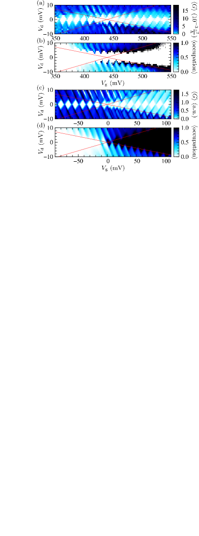
RTS (i.e. current through the trap) only occurs when the trap is in the bias window. For large gate and bias voltage excursions where the charging energy of the main dot is negligible, the main dot can be considered as part of the drain reservoir. The zone where the trap is in the bias window is then delimited by slopes and (indicated by straight lines in Fig. 7), just as for a single quantum dot. These slopes give a more straightforward access to the parameters and .
The mean occupation of the trap is higher for positive drain voltage than for negative drain voltage indicating a higher transmission rate of the trap towards source than towards the main dot.
In Fig. 7(c) and (d) we try to reproduce panels (a) and (b). For this simulation we reduce by a factor of 100 the transmission of the source barrier of the main dot when the trap is occupied. This reproduces the lines of reduced differential conductance at positive drain voltage (compare Fig. 7(a) and (c)). In the simulation the oscillations of the trap occupation decay more rapidly with bias voltage than in the measurement. This could be related to our approximation of a thermal distribution of kinetic energies in the main dot, which is certainly not accurate at high bias voltage.
Charge traps are generally believed to be not only responsible for RTS noise but also for noise in SETsJung et al. (2004) and decoherenceItakura and Tokura (2003). These interpretations imply a large number of traps with small influence on the device (in our model ). Such traps could be dopants in the reservoirs or the substrate.
VII Spin
The spin of the trap state leads via the Zeeman energy under magnetic field to a gate-voltage shift of the trap signature of:
| (4) |
is the Bohr magneton, the change in spin quantum number of the trap state in direction of the magnetic field when an electron is added to the trap. It can take the values . If there are already electrons in the trap higher changes are also possible, but they imply spin flips and such processes are therefore expected to be very slow. Weinmann et al. (1995) The Landé factor for impurities in Si and SiO2 has been measured by electron spin resonance. Lenahan and Conley (1998) The observed renormalizations are beyond the precision of our measurements, therefore we take . The gate-voltage lever-arm of the trap states is very weak as we have shown above. The Zeeman shifts should therefore be strong.
Indeed, the magnetic field clearly shifts the trap signature in Fig. 8 to lower gate voltage. In order to identify the shift as the Zeeman effect, we compare it quantitatively with the prediction of our model. The shift of the resonances due to the trap is half the peak spacing, so (see Eq. 2). The lever arm for the main dot is for this gate voltage and the width of the trap signature varies from 2.5 periods without magnetic field to 1.5 periods at . This implies a gate-voltage lever arm for the trap of (see Eq. (3)) which we interpolate as a linear function of magnetic field. The dotted line in Fig. 8 is obtained if we put this lever-arm and in Eq. (4). It is in very good agreement with the measured shift and confirms our model. The increase of the lever arm with magnetic field could be explained as follows. In the access regions the nanowire is close to the metal-insulator transition and the dopant states strongly increase the dielectric constantCastner et al. (1975). Under magnetic field they shrinkShklovskii and Efros (1984), reducing the localization length and the dielectric constant in the wire. Therefore the coupling towards the main dot and the reservoir decreases while the gate capacitance dominated by the oxide capacitance remains unaffected.
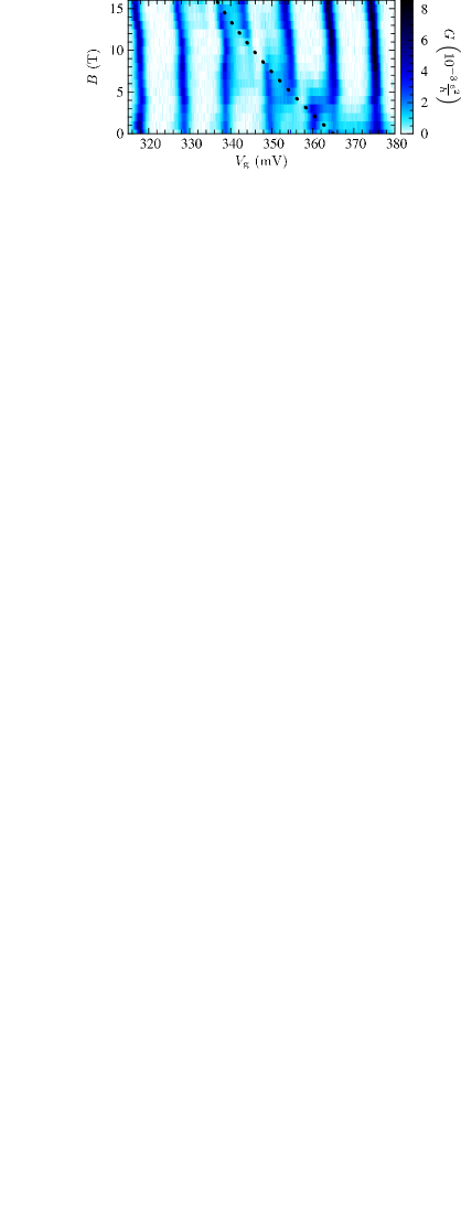
We observe such Zeeman shifts in the majority of our samples. In most cases the trap signature shifts to lower gate voltage as in Fig. 8. This is what we expect for isolated traps occupied with one electron. When a trap state is occupied with a second electron it has to occupy the energetically less favorable state whose energy is increased by the Zeeman effect. This leads to a shift towards higher gate voltage under magnetic field. Although isolated As-donor sites in Si can only be occupied by one 222Arsenic donors can be populated with 2 electrons but the second electron is so weakly bound that in the scale of our devices it can be considered as delocalized. See for example Ref. Shklovskii and Efros, 1984 electron due to Coulomb repulsion, clusters of two donors could contain two or more electrons. Bhatt and Rice (1981) For not too high doping levels clusters should however be rare. Accordingly we observe much less shifts to higher than to lower gate voltage. In devices based on similar technology Xiao et al. observed that all shifts occurred to higher gate voltageXiao et al. (2003, 2004) indicating doubly occupied traps. With precise measurements of the Landé factor they located the traps inside the oxide. This difference also supports that the traps in our device are not located in the oxide but inside the silicon wire.
VIII Perspectives
Dopant states in silicon could provide very scalable solid state quantum bits, based on charge, electron spin or nuclear spin. But it is still very difficult to control their position individually. On the other hand, with several gate electrodes one could imagine to select suitable dopants out of large number of randomly distributed dopants. In this context we have presented how the capacitance matrix of charge traps near a small silicon single electron transistor can be determined and we showed how the gate-voltage dependence of the occupation is related to the spin of the trap state and that the charge in these traps can be read out. These charge traps are attributed to arsenic dopant states. At a doping level of we observe several well isolated dopant states per device as well as percolation paths of well connected dopants linking the main quantum dot to the reservoirs. In similar geometries with multiple gate electrodes the coupling between the dopants could be tuned by changing their alignment in energy with the well connected dopants. Such randomly distributed dopants are probably more suited for electron spin quantum bits than for charge quantum bits where two dopant sites with small distance are necessary. In this perspective we are working on measurement of the coherence time of the electron spin in the observed traps. Together with the excellent stability in time as well as its full compatibility with CMOS technology our system could be a good basis for scalable quantum bits.
ACKNOWLEDGMENTS
This work was partly supported by the European Commission under the frame of the Network of Excellence “SINANO” (Silicon-based Nanodevices, IST-506844).
References
- Elzerman et al. (2004) J. M. Elzerman, R. Hanson, L. H. W. van Beveren, B. Witkamp, L. M. K. Vandersypen, and L. P. Kouwenhoven, Nature 430, 431 (2004).
- Gorman et al. (2005) J. Gorman, D. G. Hasko, and D. A. Williams, Phys. Rev. Lett. 95, 090502 (2005).
- Lafarge et al. (1991) P. Lafarge, H. Pothier, E. R. Williams, D. Estève, C. Urbina, and M. H. Devoret, Z. Phys., B 85, 327 (1991).
- Molenkamp et al. (1995) L. W. Molenkamp, K. Flensberg, and M. Kemerink, Phys. Rev. Lett. 75, 4382 (1995).
- Schoelkopf et al. (1998) R. J. Schoelkopf, P. Wahlgren, A. A. Kozhevnikov, P. Delsing, and D. E. Prober, Science 280, 1238 (1998).
- Lu et al. (2003) W. Lu, Z. Ji, L. Pfeiffer, K. W. West, and A. J. Rimber, Nature 423, 422 (2003).
- Fujisawa et al. (2004) T. Fujisawa, T. Hayashi, and Y. Hirayama, Appl. Phys. Lett. 84, 2343 (2004).
- Gustavsson et al. (2006) S. Gustavsson, R. Leturcq, B. Simovic, R. Schleser, T. Ihn, P. Studerus, K. Ensslin, D. C. Driscoll, and A. C. Gossard, Phys. Rev. Lett. 96, 076605 (2006).
- Bylander et al. (2005) J. Bylander, T. Duty, and P. Delsing, Nature 434, 361 (2005).
- Utsumi et al. (2006) Y. Utsumi, D. S. Golubev, and G. Schön, Phys. Rev. Lett. 96, 086803 (2006).
- Jung et al. (2004) S. W. Jung, T. Fujisawa, Y. Hirayama, and Y. H. Jeong, Appl. Phys. Lett. 85, 768 (2004).
- Zimmerman et al. (1997) N. M. Zimmerman, J. L. Cobb, and A. F. Clark, Phys. Rev. B 56, 7675 (1997).
- Jehl et al. (2002) X. Jehl, M. Sanquer, G. Bertrand, G. Guégan, and S. Deleonibus, J. Phys. IV France 12, 107 (2002).
- Yano et al. (1994) K. Yano, T. Ishii, T. Hashimoto, T. Kobayashi, F. Murai, and K. Seki, IEEE Trans. Electron Devices 41, 1628 (1994).
- Molas et al. (2004) G. Molas, B. D. Salvo, G. Ghibaudo, D. Mariolle, A. Toffoli, N. Buffet, R. Puglisi, S. Lombardo, and S. Deleonibus, IEEE Trans. Nanotech. 3, 42 (2004).
- Schofield et al. (2003) S. R. Schofield, N. J. Curson, M. Y. Simmons, F. J. Rueß, T. Hallam, L. Oberbeck, and R. G. Clark, Phys. Rev. Lett. 91, 136104 (2003).
- Loss and DiVincenzo (1998) D. Loss and D. P. DiVincenzo, Phys. Rev. A 57, 120 (1998).
- Kane (1998) B. E. Kane, Nature 393, 133 (1998).
- Hollenberg et al. (2004) L. C. L. Hollenberg, A. S. Dzurak, C. Wellard, A. R. Hamilton, D. J. Reilly, G. J. Milburn, and R. G. Clark, Phys. Rev. B 69, 113301 (2004).
- Tyryshkin et al. (2003) A. M. Tyryshkin, S. A. Lyon, A. V. Astashkin, and A. M. Raitsimring, Phys. Rev. B 68, 193207 (2003).
- Xiao et al. (2003) M. Xiao, I. Martin, and H. W. Jiang, Phys. Rev. Lett. 91, 078301 (2003).
- Xiao et al. (2004) M. Xiao, L. Martin, E. Yablonovitch, and H. W. Jiang, Nature 430, 435 (2004).
- Shklovskii and Efros (1984) B. I. Shklovskii and A. L. Efros, Electronic properties of doped semiconductors, no. 45 in Solid State Sciences (Springer, 1984).
- Savchenko et al. (1995) A. K. Savchenko, V. V. Kuznetsov, A. Woolfe, D. R. Mace, M. Pepper, D. A. Ritchie, and G. A. C. Jones, Phys. Rev. B 52, 17021 (1995).
- Boehm et al. (2005) M. Boehm, M. Hofheinz, X. Jehl, M. Sanquer, M. Vinet, B. Previtali, D. Fraboulet, D. Mariolle, and S. Deleonibus, Phys. Rev. B 71, 033305 (2005).
- Grupp et al. (2001) D. E. Grupp, T. Zhang, G. J. Dolan, and N. S. Wingreen, Phys. Rev. Lett. 87, 186805 (2001).
- Berkovits et al. (2005) R. Berkovits, F. von Oppen, and Y. Gefen, Phys. Rev. Lett. 94, 076802 (2005).
- Ruzin et al. (1992) I. M. Ruzin, V. Chandrasekhar, E. I. Levin, and L. I. Glazman, Phys. Rev. B 45, 13469 (1992).
- Waugh et al. (1995) F. R. Waugh, M. J. Berry, D. J. Mar, R. M. Westervelt, K. L. Campman, and A. C. Gossard, Phys. Rev. Lett. 75, 705 (1995).
- Rokhinson et al. (2002) L. P. Rokhinson, L. J. Guo, S. Y. Chou, D. C. Tsui, E. Eisenberg, R. Berkovits, and B. L. Altshuler, Phys. Rev. Lett. 88, 186801 (2002).
- Grabert and Devoret (1992) H. Grabert and M. H. Devoret, eds., Single charge tunneling: Coulomb blockade phenomena in nanostructures, vol. 294 of NATO ASI series B: Physics (Plenum Press, 1992).
- Imry et al. (1982) Y. Imry, Y. Gefen, and D. J. Bergman, Phys. Rev. B 26, 2436 (1982).
- Molas et al. (2005) G. Molas, X. Jehl, M. Sanquer, B. D. Salvo, D. Lafond, and S. Deleonibus, IEEE Trans. Nanotech. 4, 374 (2005).
- Castner et al. (1975) T. G. Castner, N. K. Lee, G. S. Cieloszyk, and G. L. Salinger, Phys. Rev. Lett. 34, 1627 (1975).
- Shafarman et al. (1989) W. N. Shafarman, D. W. Koon, and T. G. Castner, Phys. Rev. B 40, 1216 (1989).
- Kirton and Uren (1989) M. J. Kirton and M. J. Uren, Adv. Phys. 38, 367 (1989).
- Buehler et al. (2004) T. M. Buehler, D. J. Reilly, R. P. Starrett, V. C. Chan, A. R. Hamilton, A. S. Dzurak, and R. G. Clark, J. Appl. Phys. 96, 6827 (2004).
- Itakura and Tokura (2003) T. Itakura and Y. Tokura, Phys. Rev. B 67, 195320 (2003).
- Weinmann et al. (1995) D. Weinmann, W. Häusler, and B. Kramer, Phys. Rev. Lett. 74, 984 (1995).
- Lenahan and Conley (1998) P. M. Lenahan and J. F. Conley, J. Vac. Sci. Technol., B 16, 2134 (1998).
- Bhatt and Rice (1981) R. N. Bhatt and T. M. Rice, Phys. Rev. B 23, 1920 (1981).