Controlled Fabrication of Nanogaps in Ambient Environment for Molecular Electronics
Abstract
We have developed a controlled and highly reproducible method of making nanometer-spaced electrodes using electromigration in ambient lab conditions. This advance will make feasible single molecule measurements of macromolecules with tertiary and quaternary structures that do not survive the liquid-helium temperatures at which electromigration is typically performed. A second advance is that it yields gaps of desired tunnelling resistance, as opposed to the random formation at liquid-helium temperatures. Nanogap formation occurs through three regimes: First it evolves through a bulk-neck regime where electromigration is triggered at constant temperature, then to a few-atom regime characterized by conductance quantum plateaus and jumps, and finally to a tunnelling regime across the nanogap once the conductance falls below the conductance quantum.
pacs:
81.07.Lk, 73.63.RtElectromigration has recently been successfully employed to make nanometer-spaced electrodes for single molecule devices Liang et al. (2002); Park et al. (2002, 2000); Yu and Natelson (2004). The typical procedure entails an abrupt break at liquid-helium temperatures that yields a nanogap with a random tunnelling resistance Yu and Natelson (2004); Park et al. (1999); Bolton et al. (2004); Selzer et al. (2004); Lambert et al. (2003). However, this procedure makes gaps at room temperature which are typically too large for molecular measurements Bolton et al. (2004). This hinders the application of the typical electromigration procedure to molecules which do not survive a sub-freezing environment, such as macromolecules that feature modest thermodynamic stability of their respective tertiary and quaternary structures.
We have developed an electromigration procedure that is completely performed in ambient laboratory conditions and yields a controllable nanogap resistance to within a factor of about three of the target value in the 0.5 M to 1 T range. The electromigration procedure evolves through three regimes. At large conductance (), local heating increases Au mobility and triggers electromigration in the metallic neck at a critical temperature. When the neck narrows to the few-atom regime it shows jumps and plateaus near multiples of the conductance quantum () and a sharp decrease in the critical temperature. A tunnelling regime is entered once falls below accompanied by formation of a nanogap.
We first fabricate two overlapping Au leads (each 8-30 nm thick) using electron-beam lithography and double-angle evaporation of Au (Fig. 1a). An initial 3 nm thick Cr layer (deposited normal to surface) helps the contact pads adhere to the substrate while a final 40 nm thick layer of Au on the contacts reduces the resistance to between 100-200 at room temperature.
At room temperature and atmospheric pressure, we perform controlled electromigration with a succession of voltage () ramps while monitoring the current () and conductance of the leads (Fig. 2). We make an initial measurement of and compare this to later measurements as is ramped up 4 mV/sec. When decreases by a certain threshold percentage () we ramp down about 100 mV at 40 mV/sec to arrest the breaking, and then we repeat the ramping procedure to slowly form the nanogap. (We typically start with 1% and gradually increase this up to 150% as the nanogap is formed.)
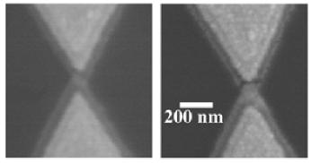
The gap conductance can be made to fall in a controlled manner to within a factor of about three of the desired value. Figure 2b shows the break to about 10 G. Figure 1b is a micrograph of a typical junction after performing the procedure. This demonstrates that a gap has clearly formed, although the location of closest approach between the electrodes is not resolved.
The reproducibility and control of the procedure permit it to be completely automated. It currently takes us between one and two hours to form a nanogap with a final resistance of about 10 G. Although can be slightly increased to form nanogaps more quickly, this seriously degrades the reproducibility of the procedure and often results in catastrophic breaks with gaps greater than 100 nm.
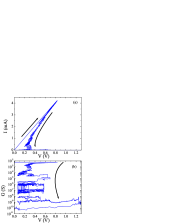
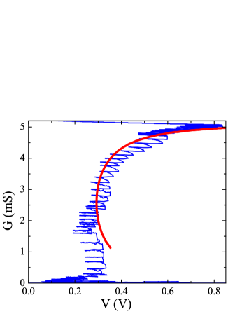
The slow gap formation permits an investigation of electromigration Christou (1994); Ho and Kwok (1989). At early stages, thermal heating accounts for the triggering of electromigration in the metallic neck. As the cross-section of the metallic neck decreases, its resistance () increases. Thus, across the neck and leads is , where is the resistance of the leads. Assigning as the critical power, the critical voltage is
| (1) |
with the conductance. can be measured independently before starting to break (as at this stage) so the only fitting parameter is the critical power. In Fig. 3, we fit Eq. 1 to the data using W. We have likewise fit data from 20 other gaps and find good agreement to the model as long as the gap conductance is larger than 1 mS (with W W). This indicates that Joule heating increases the mobility of the Au atoms in this bulk-neck regime which triggers the smoothly evolving electromigration.
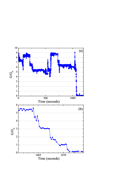
After decreases below 1 mS, electromigration occurs before reaching and the smooth evolution changes to one characterized by discrete jumps to plateaus both up and downwards by approximately . In contrast to methods using continuous mechanical strains (e.g., Refs. Muller et al., 1992, 1996; Krans et al., 1995; Olesen et al., 1994; Pascual et al., 1995), our procedure naturally leads to plateaus when ramping down which makes it difficult to discern those plateaus due to an atomic-sized neck. To circumvent this issue, Fig. 4a shows as a function of time for a junction immediately after controlled electromigration to 1.2 k, where the measurements were made with the voltage fixed at 89 mV. In such samples, we find that the conductance undergoes jumps to plateaus spaced roughly apart. As with the mechanical break junction technique Muller et al. (1996), the plateaus when often do not correspond to integral multiples of .
As falls towards , plateaus near multiples of appear. This is clearly demonstrated in Fig. 4b, which shows an expanded view of the data at the location where approaches . These plateaus are reminiscent of the quantization found with the mechanical break junction technique Muller et al. (1996). Similar to the mechanical break junction technique, we sometimes find plateaus for which do not correspond to integral multiples of , though our technique generally shows reasonable agreement with quantized conductance. Quantization implies that the metallic neck is only a few atoms wide in this regime and that a nanogap is formed once is below . We also generally find that passing below is the least controllable stage of the procedure, with the conductance sometimes abruptly falling by as much as a factor of 100 from a value near . This is further evidence that transport shifts over to tunnelling in the final nanogap regime.
It is not surprising that electromigration in the few-atom regime does not occur at , as details of atomic structure and bonding are important in this case Rubio et al. (1996); Bürki et al. (2003). As approaches , a deviation from Eq. 1 towards lower is clearly seen in the data of Fig. 3 and for those obtained from all other gaps we have made. It is likely that this failure is due to the simplicity of our model, which assumes that the dissipation occurs only in the neck and that the heat is transported away through a constant thermal conductance.
In conclusion, we have developed an electromigration procedure that can be completely performed in ambient conditions and yields a controllable nanogap resistance. This advance could considerably aid formation of electrical contacts to molecules which cannot survive sub-freezing conditions. The procedure evolves through a bulk-neck regime where electromigration is triggered at constant temperature, then to a few-atom regime characterized by quantum of conductance plateaus and jumps, and finally to a tunnelling regime once the gap is formed.
This work was supported through NSF-NIRT grant 0304531 and MRSEC-NSF grant DMR-00-79909. DJ acknowledges financial support from NSF IGERT program (grant DGE-0221664) and SENS.
References
- Liang et al. (2002) W. Liang, M. P. Shores, M. Bockrath, J. R. Long, and H. Park, Nature 417, 725 (2002).
- Park et al. (2002) J. Park, A. N. Pasupathy, J. I. Goldsmith, C. Chang, Y. Yaish, J. R. Petta, M. Rinkoski, J. P. Sethna, H. D. Abruna, P. L. McEuen, et al., Nature 417, 722 (2002).
- Park et al. (2000) H. Park, J. Park, A. K. L. Lim, E. H. Anderson, A. P. Alivisatos, and P. L. McEuen, Nature 407, 57 (2000).
- Yu and Natelson (2004) L. H. Yu and D. Natelson, Nano Letters 4, 79 (2004).
- Park et al. (1999) H. Park, A. K. L. Lim, J. Park, A. P. Alivisatos, and P. L. McEuen, Appl. Phys. Lett. 75, 301 (1999).
- Bolton et al. (2004) K. I. Bolton, F. Kuemmeth, A. N. Pasupathy, and D. C. Ralph, Appl. Phys. Lett. 84, 3154 (2004).
- Selzer et al. (2004) Y. Selzer, M. A. Cabassi, T. S. Mayer, and D. L. Allara, Nanotechnology 15, S483 (2004).
- Lambert et al. (2003) M. F. Lambert, M. F. Goffman, J. P. Bourgoin, and P. Hesto, Nanotechnology 14, 772 (2003).
- Christou (1994) A. Christou, Electromigration and Electronic Device Degradation (Wiley-Interscience, New York, 1994).
- Ho and Kwok (1989) P. S. Ho and T. Kwok, Rep. Prog. Phys. 52, 301 (1989).
- Muller et al. (1992) C. J. Muller, J. M. van Ruitenbeek, and L. J. de Jongh, Phys. Rev. Lett. 69, 140 (1992).
- Muller et al. (1996) C. J. Muller, J. M. Krans, T. N. Todorov, and M. A. Reed, Phys. Rev. B 53, 1022 (1996).
- Krans et al. (1995) J. M. Krans, J. M. van Ruitenbeek, V. V. Fisun, I. K. Yanson, and L. J. de Jongh, Nature 375, 767 (1995).
- Olesen et al. (1994) L. Olesen, E. Laegsgaard, I. Stensgaard, F. Besenbacher, J. Schiøtz, P. Stoltze, K. W. Jacobsen, and J. K. Nørskov, Phys. Rev. Lett. 72, 2251 (1994).
- Pascual et al. (1995) J. I. Pascual, J. Méndez, J. Gómez-Herrero, A. M. Baró, N. Garcia, U. Landman, W. D. Luedtke, E. N. Bogachek, and H.-P. Cheng, Science 267, 1793 (1995).
- Rubio et al. (1996) G. Rubio, N. Agraït, and S. Vieira, Phys. Rev. Lett. 76, 2302 (1996).
- Bürki et al. (2003) J. Bürki, R. E. Goldstein, and C. A. Stafford, Phys. Rev. Lett. 91, 254501 (2003).